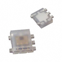
TPS851
TOSHIBA Photo-IC Silicon Epitaxial Planar
TPS851
Mobile Phones, PHS Notebook PCs, PDAs Video cameras, Digital Still Cameras Other Equipment Requiring Luminosity Adjustment
The TPS851 is an ultra-compact surface-mount photo-IC for illuminance sensors which incorporates a photodiode and current amp TOSHIBA ― circuit in a single chip. Weight: 0.0054 g (typ.) The sensitivity is superior to that of a phototransistor, and exhibits little variation. It has spectral sensitivity closer to luminous efficiency and excellent output linearity. With its ultra-compact surface-mount package, this photo-IC can be used as the power-saving control for domestic appliances or for backlighting for displays in cellular phones, this device enables low power consumption to be achieved. • • • Ultra-compact and light surface-mount package: 2.0 × 2.1 × 0.7 mm Excellent output linearity of illuminance Little fluctuation in light current and high level of sensitivity : IL = 37 μA to 74 μA @EV = 100 lx using fluorescent light : Light current variation width: ×1.67 (when light current classification is specified.) : Little temperature fluctuation • • • Built-in luminous-efficiency correction function, reduced sensitivity variations due to various light sources : IL (using incandescent light)/IL (using fluorescent light) = 1.2 (typ.) Low supply voltage, making device suitable for battery-powered equipment: VCC = 2.7 V to 5.5 V Lead(Pb)-Free
Absolute Maximum Ratings (Ta = 25°C)
Characteristics Supply voltage Output voltage Light current Permissible power dissipation Operating temperature range Storage temperature range Soldering temperature range (Note 1) Symbol VCC VOUT IL P Topr Tstg Tsol Rating −0.5 to 7 Unit V V mA mW °C °C °C
< VCC =
5 35 −30 to 85 −40 to 100 260
Note: Using continuously under heavy loads (e.g. the application of high temperature/current/voltage and the significant change in temperature, etc.) may cause this product to decrease in the reliability significantly even if the operating conditions (i.e. operating temperature/current/voltage, etc.) are within the absolute maximum ratings and the operating ranges. Please design the appropriate reliability upon reviewing the Toshiba Semiconductor Reliability Handbook (“Handling Precautions”/“Derating Concept and Methods”) and individual reliability data (i.e. reliability test report and estimated failure rate, etc). Note 1: The reflow time and the recommended temperature profile are shown in the section entitled Handling Precautions.
1
2007-10-01
�TPS851
Electrical and Optical Characteristics (Ta = 25°C)
Characteristics Supply voltage Supply current Light current (1) Symbol VCC ICC IL (1) Test Condition ⎯ VCC = 3 V, EV = 1000 lx RL = 1 kΩ VCC = 3 V, EV = 100 lx (Note 2), (Note 4) VCC = 3 V, EV = 10 lx (Note 3), (Note 4) VCC = 3 V, EV = 100 lx (Note 3), (Note 4) ⎯ (Note 2) Min 2.7 ⎯ ⎯ Typ. ⎯ 620 62 Max 5.5 ⎯ ⎯ Unit ς μA μA
Light current (2)
IL (2)
3.7
⎯
7.4
μA
Light current (3)
IL (3)
37
⎯
74
μA
Light current ratio
IL (1) IL (3) ILEAK VO
λp
⎯ ⎯
1.2
⎯
1.7 0.17
⎯ ⎯ μA
Dark current Saturation output voltage Peak sensitivity wavelength Switching time Rise time Fall time
VCC = 3.3 V, EV = 0 VCC = 3 V, RL = 150 kΩ, EV = 100 lx (Note 3)
⎯
2.2
⎯ ⎯
2.35 600 0.07 0.4
V nm ms
tr tf
VCC = 3 V, RL = 5 kΩ (Note 5)
1 2
⎯
Note 2: CIE standard A light source is used (color temperature = 2856K, approximated incandescence light). Note 3: Fluorescence light is used as light source. However, white LED is substituted in a mass-production process. IL (3) classification IL A: 37 μA to 62 μA Note 4: Light current measurement circuit
VCC IL TPS851 A OUT
Light source
Note 5: Rise time/fall time time measurement method
IF
Pulse drive White LED TPS851
VCC OUT RL
1.5 V
90%
VOUT GND 10% tr tf
2
2007-10-01
�TPS851
Package Dimensions
Unit: mm Tolerance: ±0.1 ( ): Reference value : Light-receiving area Size of light-receiving area: (□0.35 mm)
Center of sensitive area
Pin connection 1. VCC 2. GND 3. NC 4. NC 5. OUT
Weight: 0.0054 g (typ.)
Block Diagram
1. VCC
Current amp
5. OUT 2. GND 3. NC 4. NC
3
2007-10-01
�TPS851
Handling Precautions
At power-on in darkness, the internal circuit takes about 100 μs to stabilize. During this period the output signal is unstable and may change. Please take this into account.
Moisture-Proof Packing
(1) (2) To avoid moisture absorption by the resin, the product is packed in an aluminum envelope with silica gel. Since the optical characteristics of the device can be affected during soldering by vaporization resulting from prior absorption of moisture and they should therefore be stored under the following conditions: Temperature: 5°C to 30°C, Relative humidity: 60% (max), Time: 168 h (max) Baking is required if the devices have been store unopened for more than six months or if the aluminum envelope has been opened for more than 168 h. These devices are packed on tapes; hence, please avoid baking at high temperature. Recommended baking conditions: 60°C for 12 h or longer
(3)
Mounting Precautions
(1) (2) (3) Do not apply stress to the resin at high temperature. The resin part is easily scratched, so avoid friction with hard materials. When installing the assembly board in equipment, ensure that this product does not come into contact with other components.
Mounting Methods
(1) Reflow soldering • Package surface temperature: 260°C (max) • Please perform reflow soldering using the following reference temperature profile. Perform reflow soldering no more than twice.
Temperature (°C) →
260°C max 230°C 190°C 180°C Preheating part 60 s to 120 s
30 s to 50 s Heating part
Time (s) →
• •
Please perform the first reflow soldering within 168 h after opening the package with reference to the above temperature profile. Second reflow soldering In case of second reflow soldering, it should be performed within 168 h after first reflow under the above conditions. Storage conditions before second reflow soldering: 30°C, 60% RH or lower
• •
Do not perform flow soldering. Make any necessary soldering correction manually. (do not do this more than once for any given pin.) Temperature: no more than 350°C (25 W for soldering iron) Time: within 5 s
4
2007-10-01
�TPS851
(2) Recommended soldering pattern
0.65 0.65 Unit: mm
1.9
0.4
(3)
Cleaning conditions When cleaning is required after soldering Chemicals: AK225 alcohol Temperature and time: 50°C × 30 s or 30°C × 3 minutes Ultrasonic cleaning: 300 W or less
Packing Specification
(1) Packing quantity
Reel (minimum packing quantity) Carton 3,000 devices 5 reels (15,000 devices)
(2)
Packing format An aluminum envelope containing silica gel and reels is deaerated and sealed. Pack shock-absorbent materials around the aluminum envelopes in the cartons to cushion them. • Carton specification
Label
Carton dimensions (W) 81 mm × (L) 280 mm × (H) 280 mm
0.8
5
2007-10-01
�TPS851
Tape Packing Specifications
(1) Reel dimensions Reel material: Plastic
Unit: mm
11.4 9.0 5.0
φ180
φ60
5.0
Enlarged view of reel center
φ21 ± 0.8
2 ± 0.5
120°
φ13 ± 0.2
6
2007-10-01
�TPS851
(2) Tape dimensions Tape material: Plastic (anti-electrostatic)
Unit: mm Tolerance: ±0.2
φ1.5
+ 0.1 −0
4.0 ± 0.1 2.0 ± 0.1 B
1.75
0.18
(feed hole)
8.0
4.0
φ1.1
B’ 0.85 ± 0.05 Cross-section between B and B’
(pocket hole) 2.2 ± 0.05
Cross-section between A and A’
2.3 ± 0.05
A
A’
3.5 ± 0.1
7
2007-10-01
�TPS851
Reel Label
The label markings may include product number, tape type and quantity.
Sensor hole P/N TYPE ADDC NOTE TPS851 Q’TY 3,000 pcs.
Position of label
Leader and Trailer Sections of Tape
Empty trailer section: at least 10 empty device slots
Empty leader section: at least 100 mm of carrier tape Cover tape: 300 mm (min)
8
2007-10-01
�TPS851
P – Ta
40 35 1 VCC = 3 V
ILEAK – Ta
(typ.)
Power dissipation P (mW)
(μA) Dark current ILEAK
30 25 20 15 10 5 0 0
0.1
0.01
0.001
20
40
60
80
100
0.0001 20
40
60
80
100
Ambient temperature Ta (°C)
Ambient temperature Ta (°C)
IL – EV
10000
(typ.)
1.40
Relative IL – Ta
VCC = 3 V EV = 100 lx using fluorescent light
(typ.)
Light current IL (μA)
Relative light current
1000
1.20
1.00
100
0.80 10
0.60 −40 1 Ta = 25°C VCC = 3 V A light source Fluorescent light 10 100 1000 10000 10
−20
0
20
40
60
80
100
Ambient temperature Ta (°C)
0.1 1
VO – EV
(typ.)
Luminance EV (lx)
Relative IL – VCC
1.6
(typ.)
(V)
1
1.2
Relative light current
Output voltage VO
0.1
0.01
0.8
0.4
0.001
Ta = 25°C 0 2 3 4 5 6 7 0.0001 1 10
Ta = 25°C VCC = 3 V Fluorescent light Fluorescent light A light source A light source 100
RL = 1 kΩ RL = 7.5 kΩ RL = 1 kΩ RL = 7.5 kΩ 1000 10000
Supply voltage
VCC
(V)
Luminance EV (lx)
9
2007-10-01
�TPS851
ICC – EV
10000
(typ.)
1.40
Relative ICC – Ta
VCC = 3 V EV = 100 lx using fluorescent light RL = 1 kΩ
(typ.)
Relative consumption current
1000
1.20
Consumption current ICC
(μA)
1.00
100
0.80
10
1
Ta = 25°C VCC = 3 V Using the A light source RL = 250 Ω RL = 1000 Ω RL = 5000 Ω 10 100 1000 10000
0.60 −40
−20
0
20
40
60
80
100
Ambient temperature Ta (°C)
0.1 1
Luminance EV (lx)
Switching Characteristics (non-saturating operation)
1000 Ta = 25°C VCC = 3 V VOUT = 1.5 V Using white LED 300
(typ.)
1000
Switching Characteristics (saturating operation)
Ta = 25°C VCC = 3 V VOUT > 2 V = Using white LED 300
(typ.)
100
100
Switching time (μs)
30
30
Switching time (μs)
tf td 10 tr 3 ts 1 0.1
tf
10
td ts
3
tr
0.3
1
3
10
1
Load resistance RL
(kΩ)
0.3
0.1 0.1
0.3
1
3
10
Load resistance RL
(kΩ)
10
2007-10-01
�TPS851
Switching Time Measurement Circuit and Waveforms
IF td TPS851 RL VOUT GND 10% tr tf OUT 1.5 V ts 90%
Pulse drive White LED
VCC
Spectral Response
100 Ta = 25°C 80
(typ.) Luminosity angle 30°
40° 50°
Radiation Pattern
0°
(typ.) Ta = 25°C
20°
10°
10°
20°
30° 40° 50° 60° 70° 80° 90° 1.0
Relative sensitivity
60
60° 70°
40
80° 90°
20
0
0.2
0.4
0.6
0.8
0 200
400
600
800
1000
1200
Wavelength λ (nm)
11
2007-10-01
�TPS851
RESTRICTIONS ON PRODUCT USE
• The information contained herein is subject to change without notice.
20070701-EN GENERAL
• TOSHIBA is continually working to improve the quality and reliability of its products. Nevertheless, semiconductor devices in general can malfunction or fail due to their inherent electrical sensitivity and vulnerability to physical stress. It is the responsibility of the buyer, when utilizing TOSHIBA products, to comply with the standards of safety in making a safe design for the entire system, and to avoid situations in which a malfunction or failure of such TOSHIBA products could cause loss of human life, bodily injury or damage to property. In developing your designs, please ensure that TOSHIBA products are used within specified operating ranges as set forth in the most recent TOSHIBA products specifications. Also, please keep in mind the precautions and conditions set forth in the “Handling Guide for Semiconductor Devices,” or “TOSHIBA Semiconductor Reliability Handbook” etc. • The TOSHIBA products listed in this document are intended for usage in general electronics applications (computer, personal equipment, office equipment, measuring equipment, industrial robotics, domestic appliances, etc.).These TOSHIBA products are neither intended nor warranted for usage in equipment that requires extraordinarily high quality and/or reliability or a malfunction or failure of which may cause loss of human life or bodily injury (“Unintended Usage”). Unintended Usage include atomic energy control instruments, airplane or spaceship instruments, transportation instruments, traffic signal instruments, combustion control instruments, medical instruments, all types of safety devices, etc.. Unintended Usage of TOSHIBA products listed in his document shall be made at the customer’s own risk. • The products described in this document shall not be used or embedded to any downstream products of which manufacture, use and/or sale are prohibited under any applicable laws and regulations. • The information contained herein is presented only as a guide for the applications of our products. No responsibility is assumed by TOSHIBA for any infringements of patents or other rights of the third parties which may result from its use. No license is granted by implication or otherwise under any patents or other rights of TOSHIBA or the third parties. • Please contact your sales representative for product-by-product details in this document regarding RoHS compatibility. Please use these products in this document in compliance with all applicable laws and regulations that regulate the inclusion or use of controlled substances. Toshiba assumes no liability for damage or losses occurring as a result of noncompliance with applicable laws and regulations.
12
2007-10-01
�