POWER DRIVER FOR STEPPER MOTORS
INTEGRATED CIRCUITS
TMC2590 DATASHEET
Universal, cost-effective stepper driver for two-phase bipolar motors with external MOSFETs to fit
different motor sizes. With Step/Dir Interface and SPI and Stand-Alone option.
APPLICATIONS
Textile, Sewing Machines
Factory & Lab Automation
3D printing
Liquid Handling
Medical
Office Automation
Printer and Scanner
CCTV, Security
ATM, Cash recycler, POS
Pumps and Valves
Heliostat Controller
CNC Machines
FEATURES
AND
BENEFITS
Motor Current from 1A to 8A using external (N&P) MOSFETs
High Voltage Range from 5V up to 60V DC operating voltage
High Resolution up to 256 microsteps per full step
Small Size 5x5mm (body) TQFP32-EP package
Low Power Dissipation using MOSFET power stage
High Temperature Tolerance due to low self-heating
EMI-optimized slope & current controlled gate drivers
Protection & Diagnostics short to GND, short to VS /
overcurrent, programmable overtemperature & undervoltage
StallGuard2™ high precision sensorless motor load detection
CoolStep™ load dependent current control saves up to 75%
MicroPlyer™ 256 step smoothness with 1/16 step input.
SpreadCycle™ high-precision chopper for best current sine
wave form and zero crossing
Differential Current Sensing for quiet chopper operation
Resonance Dampening for mid-range velocity
BLOCK DIAGRAM
TRINAMIC Motion Control GmbH & Co. KG
Hamburg, Germany
DESCRIPTION
The TMC2590 driver for two-phase stepper
motors offers an industry-leading feature
set, including high-resolution microstepping, sensorless mechanical load measurement, load-adaptive power optimization,
and low-resonance chopper operation.
Standard SPI™ and STEP/DIR interfaces
simplify communication. The TMC2590 uses
external N- and P-channel MOSFETs for
motor currents from 1A up to roughly 8A.
No bootstrapping and charge-pump are required. Integrated protection and diagnostic features support robust and reliable
operation. High integration, high efficiency
and small form factor enable miniaturized
designs with low external component
count for cost-effective and highly
competitive
solutions.
Interfacing
is
compatible to the TMC26x family.
�TMC2590 DATASHEET (V1.01 / 2019-SEP-18)
2
APPLICATION EXAMPLES: HIGH POWER – SMALL SIZE
The TMC2590 scores with its robust design and high power density and a versatility that covers a wide
spectrum of applications and motor sizes, all while keeping costs down. Extensive support at the chip,
board, and software levels enables rapid design cycles and fast time-to-market with competitive products.
High energy efficiency from TRINAMIC’s CoolStep technology delivers further cost savings in related
systems such as power supplies and cooling. It is upward compatible to the TMC26x family of ICs and
offers higher gate driver strength than the TMC262-LA as well as additional short circuit protection and
failsafe options.
TMC2590-EVAL DEVELOPMENT PLATFORM
This evaluation board is a development platform for applications
based on the TMC2590. External power MOSFETs support drive
currents up to 4A RMS and up to 60V peak supply voltage.
The evaluation board system based on the CPU boards
LANDUNGSBRÜCKE or STARTRAMPE features an USB interface for
communication with the learning and development control
software TMCL-IDE running on a PC.
The control software provides a user-friendly GUI for setting
control parameters and visualizing the dynamic response of the
motor.
Evaluation board with 60V MOSFETs for 4A RMS
ORDER CODES
Order code
TMC2590-TA
TMC2590-TA-T
TMC2590-EVAL
ESELSBRÜCKE
LANDUNGSBRÜCKE
www.trinamic.com
PN
00-0170
00-0170T
40-0166
40-0098
40-0167
Description
CoolStep™ driver for external MOSFETs, TQFP32 (RoHS)
tape on reel packaged TMC2590-TA
Evaluation board for TMC2590
Connector board fitting to Landungsbrücke
Baseboard for TMC2590-EVAL and further evaluation
boards
Size [mm²]
5 x 5 (body)
5 x 5 (body)
85 x 55
61 x 38
85 x 55
�TMC2590 DATASHEET (V1.01 / 2019-SEP-18)
3
TABLE OF CONTENTS
1
PRINCIPLES OF OPERATION ......................... 4
1.1
1.2
1.3
1.4
2
KEY CONCEPTS ............................................... 4
CONTROL INTERFACES .................................... 5
MECHANICAL LOAD SENSING ......................... 5
CURRENT CONTROL ........................................ 5
PIN ASSIGNMENTS ........................................... 6
2.1
2.2
3
PACKAGE OUTLINE ......................................... 6
SIGNAL DESCRIPTIONS .................................. 6
INTERNAL ARCHITECTURE ............................. 8
3.1
STANDARD APPLICATION CIRCUIT .................. 9
4
STANDALONE OPERATION ...........................10
5
STALLGUARD2 LOAD MEASUREMENT .......11
5.1
5.2
5.3
5.4
6
TUNING THE STALLGUARD2 THRESHOLD ......12
STALLGUARD2 MEASUREMENT FREQUENCY
AND FILTERING ............................................13
DETECTING A MOTOR STALL ........................14
LIMITS OF STALLGUARD2 OPERATION .........14
COOLSTEP LOAD-ADAPTIVE CURRENT
CONTROL ...........................................................15
6.1
7
TUNING COOLSTEP ......................................17
SPI INTERFACE ................................................18
7.1
7.2
7.3
7.4
7.5
7.6
7.7
7.8
7.9
7.10
7.11
8
BUS SIGNALS...............................................18
BUS TIMING ................................................18
BUS ARCHITECTURE .....................................19
REGISTER WRITE COMMANDS ......................20
DRIVER CONTROL REGISTER (DRVCTRL) ....22
CHOPPER CONTROL REGISTER (CHOPCONF) ..
...................................................................24
COOLSTEP CONTROL REGISTER (SMARTEN) ...
...................................................................25
STALLGUARD2 CONTROL REGISTER
(SGCSCONF)..............................................26
DRIVER CONTROL REGISTER (DRVCONF) ...27
READ RESPONSE ..........................................29
DEVICE INITIALIZATION ...............................30
STEP/DIR INTERFACE.....................................31
8.1
8.2
8.3
8.4
8.5
9
TIMING ........................................................31
MICROSTEP TABLE .......................................32
CHANGING RESOLUTION ..............................33
MICROPLYER STEP INTERPOLATOR ...............33
STANDSTILL CURRENT REDUCTION ...............34
CURRENT SETTING ..........................................35
9.1
10
CHOPPER OPERATION ...................................37
10.1
10.2
11
SENSE RESISTORS ........................................36
SPREADCYCLE CHOPPER ...............................38
CLASSIC CONSTANT OFF-TIME CHOPPER......41
POWER MOSFET STAGE ................................43
www.trinamic.com
11.1
11.2
11.3
12
BREAK-BEFORE-MAKE LOGIC ....................... 43
ENN INPUT ................................................. 43
SLOPE CONTROL .......................................... 43
DIAGNOSTICS AND PROTECTION ............. 45
12.1
12.2
12.3
12.4
SHORT PROTECTION..................................... 45
OPEN-LOAD DETECTION .............................. 46
TEMPERATURE SENSORS............................... 47
UNDERVOLTAGE DETECTION ......................... 47
13
POWER SUPPLY SEQUENCING .................... 49
14
SYSTEM CLOCK ................................................ 49
14.1
SYSTEM CLOCK FREQUENCY ......................... 50
15
MOSFET EXAMPLES ......................................... 51
16
LAYOUT CONSIDERATIONS ......................... 52
16.1
16.2
16.3
16.4
SENSE RESISTORS ........................................ 52
EXPOSED DIE PAD....................................... 52
POWER FILTERING ....................................... 52
LAYOUT EXAMPLE ........................................ 53
17
ABSOLUTE MAXIMUM RATINGS ................. 55
18
ELECTRICAL CHARACTERISTICS ................. 56
18.1
18.2
19
OPERATIONAL RANGE .................................. 56
DC AND AC SPECIFICATIONS ...................... 56
PACKAGE MECHANICAL DATA .................... 60
19.1
19.2
DIMENSIONAL DRAWINGS ........................... 60
PACKAGE CODE............................................ 61
20
DISCLAIMER ..................................................... 62
21
ESD SENSITIVE DEVICE ................................ 62
22
TABLE OF FIGURES ......................................... 63
23
REVISION HISTORY ....................................... 64
24
REFERENCES ...................................................... 64
�TMC2590 DATASHEET (V1.01 / 2019-SEP-18)
1
4
Principles of Operation
0A+
High-Level
Interface
µC
S/D
MOSFET
TMC2590
Driver
Stage
SPI
N
0B+
0A+
TMC429
µC
S
0B-
SPI (optional)
High-Level
Interface
0A-
Motion
Controller
for up to
3 Motors
S/D
MOSFET
TMC2590
Driver
Stage
0A-
S
N
0B+
0B-
SPI (optional)
Figure 1.1 Applications block diagrams
The TMC2590 motor driver is the intelligence between a motion controller and the power MOSFETs for
driving a two-phase stepper motor, as shown in Figure 1.1. Following power-up, an embedded
microcontroller initializes the driver by sending commands over an SPI bus to write control
parameters and mode bits in the TMC2590. The microcontroller may implement the motion-control
function as shown in the upper part of the figure, or it may send commands to a dedicated motion
controller chip such as TRINAMIC’s TMC429 as shown in the lower part. For simple circuits, SPI
configuration may be omitted. The stand-alone mode configures for the most common settings.
The motion controller can control the motor position by sending pulses on the STEP signal while
indicating the direction on the DIR signal. The TMC2590 has a microstep counter and sine table to
convert these signals into the coil currents which control the position of the motor. If the
microcontroller implements the motion-control function, it can write values for the coil currents
directly to the TMC2590 over the SPI interface, in which case the STEP/DIR interface may be disabled.
This mode of operation requires software to track the motor position and reference a sine table to
calculate the coil currents.
To optimize power consumption and heat dissipation, software may also adjust CoolStep and
StallGuard2 parameters in real-time, for example to implement different tradeoffs between speed and
power consumption in different modes of operation.
The motion control function is a hard-real-time task which may be a burden to implement reliably
alongside other tasks on the embedded microcontroller. By offloading the motion-control function to
the TMC429, up to three motors can be operated reliably with very little demand for service from the
microcontroller. Software only needs to send target positions, and the TMC429 generates precisely
timed step pulses. Software retains full control over both the TMC2590 and TMC429 through the SPI
bus.
1.1 Key Concepts
The TMC2590 motor driver implements several advanced patented features which are exclusive to
TRINAMIC products. These features contribute toward greater precision, greater energy efficiency,
higher reliability, smoother motion, and cooler operation in many stepper motor applications.
StallGuard2™
High-precision load measurement using the back EMF on the coils
CoolStep™
Load-adaptive current control which reduces energy consumption by as much as
75%
SpreadCycle™
High-precision chopper algorithm available as an alternative to the traditional
constant off-time algorithm
MicroPlyer™
Microstep interpolator for obtaining increased smoothness of microstepping over a
STEP/DIR interface
www.trinamic.com
�TMC2590 DATASHEET (V1.01 / 2019-SEP-18)
5
In addition to these performance enhancements, TRINAMIC motor drivers also offer safeguards to
detect and protect against shorted outputs, open-circuit output, overtemperature, and undervoltage
conditions for enhancing safety and recovery from equipment malfunctions.
1.2 Control Interfaces
There are two control interfaces from the motion controller to the motor driver: the SPI serial
interface and the STEP/DIR interface. The SPI interface is used to write control information to the chip
and read back status information. This interface allows application specific initialization of parameters
and modes. This interface may also be used for directly setting the currents flowing through the
motor coils, as an alternative to stepping the motor using the STEP and DIR signals, so the motor can
be controlled through the SPI interface alone.
In stand-alone mode, the most common configuration is pre-loaded automatically. The three SPI
inputs allow for additional choices.
The STEP/DIR interface allow universal real-time-control and is simple and robust.
1.2.1 SPI Interface
The SPI interface is a bit-serial interface synchronous to a bus clock. For every bit sent from the bus
master to the bus slave, another bit is sent simultaneously from the slave to the master.
Communication between an SPI master and the TMC2590 slave always consists of sending one 20-bit
command word and receiving one 20-bit status word.
1.2.2 Stand-Alone Control
Three configuration lines set 16 or 256 microsteps, chopper hysteresis, to adapt for motor size, and
motor current (2-level). With this, basic configuration of the driver does not require any interfacing.
1.2.3 STEP/DIR Interface
The STEP/DIR interface is enabled by default. Active edges on the STEP input can be rising edges or
both rising and falling edges, as controlled by the mode bit (DEDGE). Using both edges cuts the
toggle rate of the STEP signal in half, which is useful for communication over slow interfaces such as
optically isolated interfaces.
On each active edge, the state sampled from the DIR input determines whether to step forward or
back. Each step can be a fullstep or a microstep, in which there are 2, 4, 8, 16, 32, 64, 128, or 256
microsteps per fullstep. During microstepping, a low state on DIR increases the microstep counter and
a high decreases the counter by an amount controlled by the microstep resolution. An internal table
translates the counter value into the sine and cosine values which control the motor current for
microstepping.
1.3 Mechanical Load Sensing
The TMC2590 provides StallGuard2 high-resolution load measurement for determining the mechanical
load on the motor by measuring the back EMF. In addition to detecting when a motor stalls, this
feature can be used for homing to a mechanical stop without a limit switch or proximity detector. The
CoolStep power-saving mechanism uses StallGuard2 to reduce the motor current to the minimum
motor current required to meet the actual load placed on the motor.
1.4 Current Control
Current into the motor coils is controlled using a cycle-by-cycle chopper mode. Two chopper modes
are available: a traditional constant off-time mode and the new SpreadCycle mode. SpreadCycle mode
offers smoother operation and greater power efficiency over a wide range of speed and load.
www.trinamic.com
�TMC2590 DATASHEET (V1.01 / 2019-SEP-18)
2
6
Pin Assignments
TST_MODE
STEP
DIR
VCC_IO
SRAL
SG_TST
ST_ALONE
VS
32
31
30
29
28
27
26
25
2.1 Package Outline
GND
1
24
VHS
HA1
2
23
HB1
HA2
3
22
HB2
BMA2
4
21
BMB2
BMA1
5
20
BMB1
LA1
6
19
LB1
18
LB2
17
SRB
10
11
12
13
14
15
16
SDI
SCK
SRBL
CSN
ENN
CLK
8
SDO
SRA
9
7
PAD = GND
5VOUT
LA2
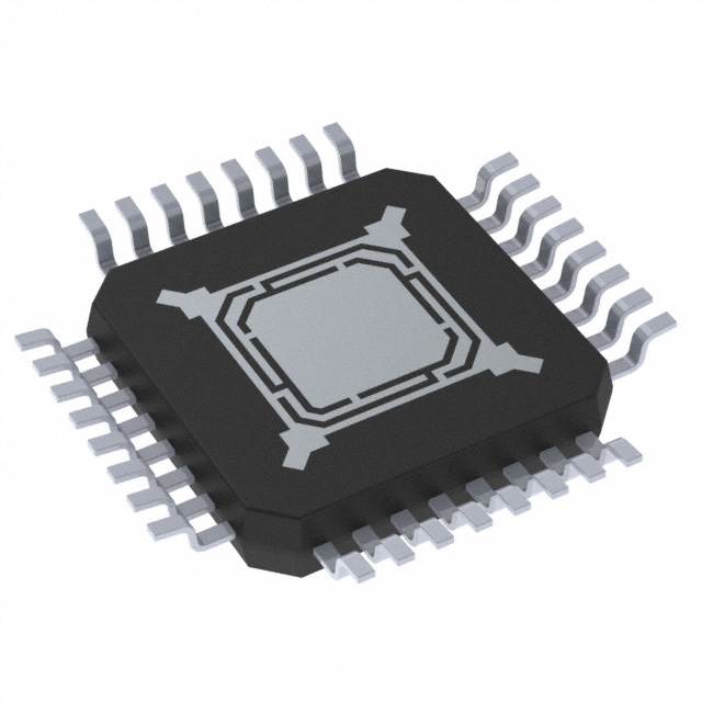
TMC2590-TA
TQFP-32
7mm x 7mm
Figure 2.1 TMC2590 pin assignments
2.2 Signal Descriptions
Pin
GND
HA1
HA2
HB1
HB2
BMA1
BMA2
BMB1
BMB2
LA1
Number
1
PAD
2
3
23
22
5
4
20
21
6
www.trinamic.com
Type
O (VS)
Function
Digital and analog low power GND. Connect both to PCB GND
plane.
High side P-channel driver output. Becomes driven to VHS to switch
on MOSFET.
I (VS)
Sensing input for bridge outputs. Used for short detection. Connect
to center of the respective half-bridge.
O 5V
Low side MOSFET driver output. Becomes driven to 5VOUT to switch
�TMC2590 DATASHEET (V1.01 / 2019-SEP-18)
Pin
LA2
LB1
LB2
SRA
SRB
SRAL
SRBL
Number
7
19
18
8
17
28
13
5VOUT
9
SDO
SDI (CFG3)
10
11
DO VIO
DI VIO
SCK (CFG2)
12
DI VIO
CSN (CFG1)
14
DI VIO
ENN
15
DI VIO
CLK
16
DI VIO
VHS
24
VS
25
ST_ALONE
26
DI VIO
(pd)
SG_TST
27
DO VIO
VCC_IO
29
DIR
30
DI VIO
STEP
TST_MODE
31
32
DI VIO
DI VIO
(pd)
www.trinamic.com
7
Type
Function
on MOSFET.
AI
Sense resistor input for coil current measurement. Connect to upper
side of sense resistor.
Sense resistor negative input for coil current measurement. For best
results, connect to lower side of sense resistor using Kelvin
connection, or connect to GND plane near the respective sense
resistor’s GND terminal.
Output of internal 5V linear regulator. This voltage is used to
supply the low side drivers and internal analog circuitry. An
external capacitor to GND close to the pin is required. Place the
capacitor near to pin 9. 470nF ceramic are sufficient for most
applications, a higher capacity up to 10µF improves performance
with high gate charge MOSFETs.
Data output of SPI interface (Tristate)
Data input of SPI interface /
Microstep resolution control input in standalone mode:
0: MRES=256 microsteps; 1: MRES=16 microsteps with interpolation
Serial clock input of SPI interface /
Chopper hysteresis control input in standalone mode:
0: HEND=4, HSTRT=2; 1: HEND=4, HSTRT=6
Chip select input of SPI interface /
Current control input in standalone mode:
0: Current scale CS=15; 1: Current scale CS=31
Enable not input for drivers. Switches off all MOSFETs. Tie low for
normal operation.
Clock input for all internal operations. Tie low to use internal
oscillator. Automatically switches to external clock, when the first
high signal is recognized.
High side supply voltage (motor supply voltage VS - 10V). Attach a
ceramic capacitor between VHS and VS. Typ. 220nF to 1µF, 16V.
Motor supply voltage. Tie to positive supply voltage of MOSFET
bridge.
Stand-alone mode selection. Tie to VCC_IO for non-SPI, stand-alone
mode. Leave open for normal operation. Internal 10k pulldown
resistor.
StallGuard2™ output. Signals motor stall (high active). Evaluate only
when at sufficient velocity.
Input / output supply voltage VIO for all digital pins. Tie to digital
logic supply voltage. Allows operation in 3.3V and 5V systems.
Direction input. Is sampled upon detection of a step to determine
stepping direction. An internal glitch filter for 20ns is provided.
Step input. An internal glitch filter for 20ns is provided.
Test mode input. Puts IC into test mode. Tie to GND for normal
operation using a short wire to GND plane. Internal 166k pull down
resistor for safety. No user functionality.
AI
�TMC2590 DATASHEET (V1.01 / 2019-SEP-18)
3
8
Internal Architecture
Figure 3.1 shows the internal architecture of the TMC2590.
+VM 9-59V
220n
16V
VHS
TMC2590
+VCC
3.3V or 5V
VCC_IO
VM-10V
linear
regulator
OSC
15MHz
D
100n
8-20MHz
100n
VS
5V linear
regulator
CLK
STEP
DIR
Clock selector
P-Gate
drivers
D
SCK
SDI
SDO
Phase polarity
SIN &
COS
Chopper
logic
Break
before
make
Short
detectors
N-Gate
drivers
SG_TST
G
S
G
P
P
D
BMA2
motor coil A
D
LA2
D
N
G
N
G
S
LA1
S
SRA
VREF
D
D
Digital control
9
M
U
X
D
D
SPI interface
DAC
RSENSE
100mOhm for 2.8A peak
(resp. 1.5A RMS)
RSENSE
100mOhm for 2.8A peak
(resp. 1.5A RMS)
SRAL
DAC
SRBL
slope LS
+5V
D
D
47R
+5V
optional input protection resistors
against inductive sparks upon
motor cable break
9
D
slope LS
47R
SRB
CoolStep
Energy
efficiency
stallGuard
output
S
HA2
BMA1
VSENSE
CSN
SPI /
Stand-alone
configuration
HA1
D
0.16V
0.30V
ENN
+VM
CLK
Step &
Direction
interface
D
Sine wave
1024 entry
ST_ALONE
Provide sufficient filtering capacity near
bridge transistors (electrolyt capacitors
and ceramic capacitors)
slope HS VHS
D
Step multiply
16 to 256
Open or GND for
SPI, VCC_IO for
stand-alone
5V supply
470nF
ENABLE
step & dir
(optional)
5VOUT
N-Gate
drivers
stallGuard 2
BACK
EMF
Protection &
Diagnostics
SHORT TO
GND
Phase polarity
Chopper
logic
Break
before
make
Short
detectors
LB1
S
G
LB2
S
G
N
D
N
D
motor coil B
BMB2
BMB1
D
P-Gate
drivers
ENABLE
Temp. sensor
100°C, 120°C,
136°C, 150°C
slope HS VHS
DIE PAD
GND
HB2
D
P
G
P
G
S
S
HB1
+VM
TST_MODE
Figure 3.1 TMC2590 block diagram and application schematic
Prominent features include:
Oscillator and clock selector
Step and direction interface
SPI interface
Multiplexer
Multipliers
DACs and comparators
Break-before-make and gate drivers
On-chip voltage regulators
www.trinamic.com
provides the system clock from the on-chip oscillator or an external
source.
uses a microstep counter and sine table to generate target currents
for the coils.
receives commands for configuration or commands that directly set
the coil current values.
selects either the output of the sine table or the SPI interface for
controlling the current into the motor coils.
scales down the currents to both coils when the currents are
greater than those required by the load on the motor or as set by
the CS current scale parameter.
converts the digital current values to analog signals that are
compared with the voltages on the sense resistors. Comparator
outputs terminate chopper drive phases when target currents are
reached.
ensure non-overlapping pulses, boost drive voltage, and control
pulse slope to the gates of the power MOSFETs.
provide high-side voltage for P-channel MOSFET gate drivers and
supply voltage for on-chip analog and digital circuits.
�TMC2590 DATASHEET (V1.01 / 2019-SEP-18)
9
3.1 Standard Application circuit
+VM
+VM
CE
DIR
STEP
Must be identical to
bridge supply!
VS
VS
5VOUT
2.2µ
CSN
SCK
SDI
SDO
SG_TST
LS
BMB1
LB1
LB2
LS
SRBH
SPI interface
47R
RS
SRBL
stallGuard2
S
Chopper
+VM
B.Dwersteg, ©
TRINAMIC 2014
HS
VHS
CLK
HA2
N
stepper
motor
470n
HA1
HS
opt. ext. clock
12-16MHz
470n
BMB2
TMC2590
Sequencer
Stall detection pulse
(react to first impulse /
ignore outside velocity
window)
HB2
HB1
HS
5V Voltage
regulator
C5VOUT: 470nF to 10µF
(higher for lower noise chopper)
CVHS: 220nF to 1µF
(both higher for higher MOSFET gate
charge)
SPI interface for
configuration or for driving
(optional to Step/Dir)
Configuration pins in stand
alone mode
HS
Step&Dir input
with microPlyer
VHS
100n
VS-10V
regulator
5V
220n
VS
VHS
BMA1
5V
BMA2
+VIO
3.3V or 5V
I/O voltage
LS
VCC_IO
LS
100n
LA1
SRAH
mode selection
SRAL
Opt. stand alone
configuration
47R
RS
Use low inductivity SMD
type, e.g. 1210 or 2512
resistor for RS!
GND
DIE PAD
TST_MODE
pd
DRV_ENN
ST_ALONE
pd
Keep inductivity of the fat
interconnections as small as
possible to avoid ringing!
LA2
opt. driver enable
Figure 2 Standard application circuit
The standard application uses a minimum number of external components in order to operate the
stepper motor. Four N-channel and four P-channel MOSFETs are required, and shall be selected as
required for the application motor current. See chapter 15 for examples. With N&P channel FETs, no
charge-pump is required, making the design small and robust. Two sense resistors set the motor coil
current. See chapter 9 for the calculation of the right sense resistor value. Use low ESR capacitors for
filtering the power supply. A minimum of 100µF per ampere of coil current near to the power bridge
is recommended for best performance. These capacitors need to cope with the current ripple caused
by chopper operation, thus they should not be dimensioned too small. Current ripple in the supply
capacitors also depends on the power supply internal resistance and cable length. VCC_IO can be
supplied from 5VOUT, or from an external source, e.g. 3.3V.
Basic layout hints
Place sense resistors and all filter capacitors as close as possible to the power MOSFETs. Place the
TMC2590 near to the MOSFETs and use short interconnection lines in order to minimize parasitic trace
inductance. Use a solid common GND for GND and die pad GND connections, also for sense resistor
GND. Connect 5VOUT filtering capacitor directly to 5VOUT and GND plane. See layout hints for more
details. High capacity ceramic or low ESR electrolytic capacitors are recommended for VS filtering.
www.trinamic.com
�TMC2590 DATASHEET (V1.01 / 2019-SEP-18)
4
10
Standalone Operation
Standalone operation is the easiest way to use the IC. In this mode, three pins configure for the most
common settings. Just use the standard application circuit, tie low / high the SPI input pins to set the
desired basic operation parameters and choose a sense resistor to fit the required motor current.
However, advanced configuration and access to individual diagnostics only is possible via SPI.
CSN: SELECTION OF MOTOR CURRENT (USE FOR STANDSTILL CURRENT REDUCTION)
CSN (CFG1)
GND
Chopper Setting
Current Scale CS=15.
Use for standstill current reduction, or to adapt lower sense resistor value.
Current Scale CS=31.
Maximum current. Control motor current by adapting sense resistors.
VCC_IO
SCK: SELECTION OF CHOPPER HYSTERESIS (ADAPT FOR LOWEST MOTOR NOISE & VIBRATION)
SCK (CFG2)
GND
VCC_IO
Chopper Setting
Low hysteresis (HSTRT=2, HEND=4), use for larger motor.
Medium hysteresis (HSTRT=6, HEND=4), typical for Nema17 or smaller motor, or
for high speed motors with high coil currents.
SDI: SELECTION OF MICROSTEP RESOLUTION (ADAPT TO STEP PULSE GENERATOR)
SDI (CFG3)
GND
VCC_IO
Chopper Setting
256 Microsteps full resolution for Step/Dir interface
16 Microsteps with internal interpolation to 256 microsteps
+VM
VCC_IO
STEP
DIR
Current
Hysteresis
Microsteps
TMC2590
Step Multiplier
+VCCIO
Gate driver
Gate Driver
Sine Table
4*256 entry
ST_ALONE
Stand Alone
CSN/CFG1
SCK/CFG2
SDI/CFG3
SPI control,
Config & Diags
x
ENN
Protection
& Diagnostics
S
Chopper
N
BM
Gate driver
Gate Driver
2 Phase Stepper
LS
coolStep
RS
SDO
Enable/
Disable
HS
stallGuard2
2 x Current
Comparator
2 x DAC
RS
RS
SG_TST
Figure 3 Standalone configuration
Standalone mode automatically enables resonance dampening (EN_PFD) and 136°C overtemperature
detection (OT_SENSE), sensitive high-side short detection (SHRTSENSE) and enable low side short
protection (S2VS). Driver strength becomes set to SLPL=SLPH=3. TOFF is 4, TBL is 36 clocks in this
mode. All other bits are cleared to 0.
In standalone configuration, StallGuard level is fixed to SGT=2. This setting will work for homing with
many 42mm and larger motors in a suitable velocity range. Adapt to full or half current as fitting
using CSN configuration pin.
Resulting configuration words:
SDI=0: $00200 / SDI=1: $00204
SCK=0: $90224 / SCK=1: $90264
CSN=0: $C020F / CSN=1: $C021F
$E810F, $A0000
www.trinamic.com
�TMC2590 DATASHEET (V1.01 / 2019-SEP-18)
5
11
StallGuard2 Load Measurement
StallGuard2 provides an accurate measurement of the load on the motor within a selected velocity
range. It can be used for stall detection as well as other uses at loads below those which stall the
motor, such as CoolStep load-adaptive current reduction. (StallGuard2 is a more precise evolution of
the earlier StallGuard technology.)
The StallGuard2 measurement value changes linearly over a wide range of load, velocity, and current
settings, as shown in Figure 5.1. At maximum motor load, the value goes to zero or near to zero. This
corresponds to a load angle of 90° between the magnetic field of the coils and magnets in the rotor.
This also is the most energy-efficient point of operation for the motor.
1000
stallGuard2
reading
900
Start value depends
on motor and
operating conditions
800
700
600
stallGuard value reaches zero
and indicates danger of stall.
This point is set by stallGuard
threshold value SGT.
500
400
Motor stalls above this point.
Load angle exceeds 90° and
available torque sinks.
300
200
100
0
10
20
30
40
50
60
70
80
90
100
motor load
(% max. torque)
Figure 5.1 StallGuard2 load measurement SG as a function of load
Two parameters control StallGuard2 and one status value is returned.
Parameter
SGT
SFILT
Description
7-bit signed integer that sets the StallGuard2
threshold level for asserting the SG_TST output
and sets the optimum measurement range for
readout. Negative values increase sensitivity,
and positive values reduce sensitivity so more
torque is required to indicate a stall. Zero is a
good starting value.
Mode bit which enables the StallGuard2 filter for
more precision. If set, reduces the measurement
frequency to one measurement per four
fullsteps. If cleared, no filtering is performed.
Filtering
compensates
for
mechanical
asymmetries in the construction of the motor,
but at the expense of response time. Unfiltered
operation is recommended for rapid stall
detection. Filtered operation is recommended
for more precise load measurement.
www.trinamic.com
Setting
0
Comment
indifferent value
+1… +63
less sensitivity
-1… -64
higher sensitivity
0
1
standard mode
filtered mode
�TMC2590 DATASHEET (V1.01 / 2019-SEP-18)
Status word
SG
Description
10-bit unsigned integer StallGuard2 measurement result. A higher value indicates lower
mechanical load. A lower value indicates a
higher load and therefore a higher load angle.
For stall detection, adjust SGT to return an SG
value of 0 or slightly higher upon maximum
motor load before stall.
12
Range
0… 1023
Comment
0: highest load
low value: high load
high value: less load
5.1 Tuning the StallGuard2 Threshold
Due to the dependency of the StallGuard2 value SG from motor-specific characteristics and applicationspecific demands on load and velocity the easiest way to tune the StallGuard2 threshold SGT for a
specific motor type and operating conditions is interactive tuning in the actual application.
The procedure is:
1.
2.
3.
Operate the motor at a reasonable velocity for your application and monitor SG.
Apply slowly increasing mechanical load to the motor. If the motor stalls before SG reaches
zero, decrease SGT. If SG reaches zero before the motor stalls, increase SGT. A good SGT
starting value is zero. SGT is signed, so it can have negative or positive values.
The optimum setting is reached when SG is between 0 and 400 at increasing load shortly
before the motor stalls, and SG increases by 100 or more without load. SGT in most cases can
be tuned together with the motion velocity in a way that SG goes to zero when the motor
stalls and the stall output SG_TST is asserted. This indicates that a step has been lost.
The system clock frequency affects SG. An external crystal-stabilized clock should be used for
applications that demand the highest performance. The power supply voltage also affects SG, so
tighter regulation results in more accurate values. SG measurement has a high resolution, and there
are a few ways to enhance its accuracy, as described in the following sections.
5.1.1 Variable Velocity Operation
Across a range of velocities, on-the-fly adjustment of the StallGuard2 threshold SGT improves the
accuracy of the load measurement SG. This also improves the power reduction provided by CoolStep,
which is driven by SG. Linear interpolation between two SGT values optimized at different velocities is
a simple algorithm for obtaining most of the benefits of on-the-fly SGT adjustment, as shown in
Figure 5.2. This figure shows an optimal SGT curve in black and a two-point interpolated SGT curve in
red.
www.trinamic.com
�TMC2590 DATASHEET (V1.01 / 2019-SEP-18)
stallGuard2
reading at
no load
optimum
SGT setting
simplified
SGT setting
1000
20
900
18
800
16
700
14
600
12
500
10
400
8
300
6
200
4
100
2
0
0
50
lower limit for stall
detection 4 RPM
100
150
13
200
250
300
350
400
450
back EMF reaches
supply voltage
500
550
600
Motor RPM
(200 FS motor)
Figure 5.2 Linear interpolation for optimizing SGT with changes in velocity
5.1.2 Small Motors with High Torque Ripple and Resonance
Motors with a high detent torque show an increased variation of the StallGuard2 measurement value
SG with varying motor currents, especially at low currents. For these motors, the current dependency
might need correction in a similar manner to velocity correction for obtaining the highest accuracy.
5.1.3 Temperature Dependence of Motor Coil Resistance
Motors working over a wide temperature range may require temperature correction, because motor
coil resistance increases with rising temperature. This can be corrected as a linear reduction of SG at
increasing temperature, as motor efficiency is reduced.
5.1.4 Accuracy and Reproducibility of StallGuard2 Measurement
In a production environment, it may be desirable to use a fixed SGT value within an application for
one motor type. Most of the unit-to-unit variation in StallGuard2 measurements results from
manufacturing tolerances in motor construction. The measurement error of StallGuard2 – provided
that all other parameters remain stable – can be as low as:
𝑠𝑡𝑎𝑙𝑙𝐺𝑢𝑎𝑟𝑑 𝑚𝑒𝑎𝑠𝑢𝑟𝑒𝑚𝑒𝑛𝑡 𝑒𝑟𝑟𝑜𝑟 = ±𝑚𝑎𝑥(1, |𝑆𝐺𝑇|)
5.2 StallGuard2 Measurement Frequency and Filtering
The StallGuard2 measurement value SG is updated with each full step of the motor. This is enough to
safely detect a stall, because a stall always means the loss of four full steps. In a practical application,
especially when using CoolStep, a more precise measurement might be more important than an
update for each fullstep because the mechanical load never changes instantaneously from one step to
the next. For these applications, the SFILT bit enables a filtering function over four load
measurements. The filter should always be enabled when high-precision measurement is required. It
compensates for variations in motor construction, for example due to misalignment of the phase A to
phase B magnets. The filter should only be disabled when rapid response to increasing load is
required, such as for stall detection at high velocity.
www.trinamic.com
�TMC2590 DATASHEET (V1.01 / 2019-SEP-18)
14
5.3 Detecting a Motor Stall
To safely detect a motor stall, a stall threshold must be determined using a specific SGT setting.
Therefore, you need to determine the maximum load the motor can drive without stalling and to
monitor the SG value at this load, for example some value within the range 0 to 400. The stall
threshold should be a value safely within the operating limits, to allow for parameter stray. So, your
microcontroller software should set a stall threshold which is slightly higher than the minimum value
seen before an actual motor stall occurs. The response at an SGT setting at or near 0 gives some idea
on the quality of the signal: Check the SG value without load and with maximum load. These values
should show a difference of at least 100 or a few 100, which shall be large compared to the offset. If
you set the SGT value so that a reading of 0 occurs at maximum motor load, an active high stall
output signal will be available at SG_TST output.
5.4 Limits of StallGuard2 Operation
StallGuard2 does not operate reliably at extreme motor velocities: Very low motor velocities (for many
motors, less than one revolution per second) generate a low back EMF and make the measurement
unstable and dependent on environment conditions (temperature, etc.). Other conditions will also lead
to extreme settings of SGT and poor response of the measurement value SG to the motor load.
Very high motor velocities, in which the full sinusoidal current is not driven into the motor coils also
lead to poor response. These velocities are typically characterized by the motor back EMF reaching the
supply voltage.
www.trinamic.com
�TMC2590 DATASHEET (V1.01 / 2019-SEP-18)
6
15
CoolStep Load-Adaptive Current Control
CoolStep allows substantial energy savings, especially for motors which see varying loads or operate
at a high duty cycle. Because a stepper motor application needs to work with a torque reserve of 30%
to 50%, even a constant-load application allows significant energy savings because CoolStep
automatically enables torque reserve when required. Reducing power consumption keeps the system
cooler, increases motor life, and allows reducing cost in the power supply and cooling components.
Hint
Reducing motor current by half results in reducing power by a factor of four.
Energy efficiency
Motor generates less heat
Less cooling infrastructure
Cheaper motor
-
power consumption decreased up to 75%.
improved mechanical precision.
for motor and driver.
does the job.
0,9
Efficiency with coolStep
0,8
Efficiency with 50% torque reserve
0,7
0,6
0,5
Efficiency
0,4
0,3
0,2
0,1
0
0
50
100
150
200
250
300
350
Velocity [RPM]
Figure 6.1 Energy efficiency example with CoolStep
Figure 6.1 shows the efficiency gain of a 42mm stepper motor when using CoolStep compared to
standard operation with 50% of torque reserve. CoolStep is enabled above 60rpm in the example.
CoolStep is controlled by several parameters, but two are critical for understanding how it works:
Parameter
SEMIN
SEMAX
Description
Range
4-bit unsigned integer that sets a lower 0… 15
threshold. If SG goes below this threshold,
CoolStep increases the current to both coils. The
4-bit SEMIN value is scaled by 32 to cover the
lower half of the range of the 10-bit SG value.
(The name of this parameter is derived from
smartEnergy, which is an earlier name for
CoolStep.)
4-bit unsigned integer that controls an upper 0… 15
threshold. If SG is sampled equal to or above
this threshold enough times, CoolStep decreases
the current to both coils. The upper threshold is
(SEMIN + SEMAX + 1) x 32.
www.trinamic.com
Comment
lower StallGuard
threshold:
SEMINx32
upper StallGuard
threshold:
(SEMIN+SEMAX+1)x32
�TMC2590 DATASHEET (V1.01 / 2019-SEP-18)
16
mechanical load
stallGuard2
reading
motor current
Figure 6.2 shows the operating regions of CoolStep. The black line represents the SG measurement
value, the blue line represents the mechanical load applied to the motor, and the red line represents
the current into the motor coils. When the load increases, SG falls below SEMIN, and CoolStep
increases the current. When the load decreases and SG rises above (SEMIN + SEMAX + 1) x 32 the
current becomes reduced.
current setting CS
(upper limit)
motor current reduction area
SEMAX+SEMIN+1
SEMIN
½ or ¼ CS
(lower limit)
motor current increment area
0=maximum load
load angle optimized
time
slow current reduction due
to reduced motor load
load
angle
optimized
current increment due to
increased load
stall possible
load angle optimized
Figure 6.2 CoolStep adapts motor current to the load
Four more parameters control CoolStep and one status value is returned:
Parameter
CS
SEUP
SEDN
SEIMIN
Status word
SE
Description
Current scale. Scales both coil current values as
taken from the internal sine wave table or from
the SPI interface. For high precision motor
operation, work with a current scaling factor in
the range 16 to 31, because scaling down the
current values reduces the effective microstep
resolution by making microsteps coarser. This
setting also controls the maximum current value
set by CoolStep™.
Number of increments of the coil current for each
occurrence of an SG measurement below the
lower threshold.
Number of occurrences of SG measurements
above the upper threshold before the coil current
is decremented.
Mode bit that controls the lower limit for scaling
the coil current. If the bit is set, the limit is ¼
CS. If the bit is clear, the limit is ½ CS.
Range
Comment
0… 31
scaling factor:
1/32, 2/32, … 32/32
0… 3
step width is:
1, 2, 4, 8
0… 3
number of StallGuard
measurements per
decrement: 32, 8, 2, 1
Minimum motor
current: 1/2 of CS
1/4 of CS
Comment
Actual motor current
scaling factor set by
CoolStep:
1/32, 2/32, … 32/32
0
1
Description
Range
5-bit unsigned integer reporting the actual cur- 0… 31
rent scaling value determined by CoolStep. This
value is biased by 1 and divided by 32, so the
range is 1/32 to 32/32. The value will not be
greater than the value of CS or lower than either
¼ CS or ½ CS depending on SEIMIN setting.
www.trinamic.com
�TMC2590 DATASHEET (V1.01 / 2019-SEP-18)
17
6.1 Tuning CoolStep
Before tuning CoolStep, first tune the StallGuard2 threshold level SGT, which affects the range of the
load measurement value SG. CoolStep uses SG to operate the motor near the optimum load angle of
+90°.
The current increment speed is specified in SEUP, and the current decrement speed is specified in
SEDN. They can be tuned separately because they are triggered by different events that may need
different responses. The encodings for these parameters allow the coil currents to be increased much
more quickly than decreased, because crossing the lower threshold is a more serious event that may
require a faster response. If the response is too slow, the motor may stall. In contrast, a slow
response to crossing the upper threshold does not risk anything more serious than missing an
opportunity to save power.
Hint
CoolStep operates between limits controlled by the current scale parameter CS and the SEIMIN bit.
6.1.1 Response Time
For fast response to increasing motor load, use a high current increment step SEUP. If the motor load
changes slowly, a lower current increment step can be used to avoid motor current oscillations. If the
filter controlled by SFILT is enabled, the measurement rate and regulation speed are cut by a factor of
four.
6.1.2 Low Velocity and Standby Operation
Because StallGuard2 is not able to measure the motor load in standstill and at very low RPM, the
current at low velocities should be set to an application-specific default value and combined with
standstill current reduction settings programmed through the SPI interface.
www.trinamic.com
�TMC2590 DATASHEET (V1.01 / 2019-SEP-18)
7
18
SPI Interface
The TMC2590 allows full control over all configuration parameters and mode bits through the SPI
interface. In SPI mode, initialization is required prior to motor operation. The SPI interface also allows
reading back status values and bits.
7.1 Bus Signals
The SPI bus on the TMC2590 has four signals:
SCK
SDI
SDO
CSN
bus clock input
serial data input
serial data output
chip select input (active low)
The slave is enabled for an SPI transaction by a low on the chip select input CSN. Bit transfer is
synchronous to the bus clock SCK, with the slave latching the data from SDI on the rising edge of SCK
and driving data to SDO following the falling edge. The most significant bit is sent first. A minimum
of 20 SCK clock cycles is required for a bus transaction with the TMC2590.
If more than 20 clocks are driven, the additional bits shifted into SDI are shifted out on SDO after a
20-clock delay through an internal shift register. This can be used for daisy chaining multiple chips.
CSN must be low during the whole bus transaction. When CSN goes high, the contents of the internal
shift register are latched into the internal control register and recognized as a command from the
master to the slave. If more than 20 bits are sent, only the last 20 bits received before the rising edge
of CSN are recognized as the command.
7.2 Bus Timing
SPI interface is synchronized to the internal system clock, which limits the SPI bus clock SCK to half
of the system clock frequency. If the system clock is based on the on-chip oscillator, an additional
10% safety margin must be used to ensure reliable data transmission. All SPI inputs as well as the
ENN input are internally filtered to avoid triggering on pulses shorter than 20ns. Figure 7.1 shows the
timing parameters of an SPI bus transaction, and the table below specifies their values.
CSN
tCC
tCL
tCH
tCH
tCC
SCK
tDU
SDI
bit19
tDH
bit18
bit0
tDO
SDO
tZC
bit19
Figure 7.1 SPI Timing
Hint
Usually this SPI timing is referred to as SPI MODE 3
www.trinamic.com
bit18
bit0
�TMC2590 DATASHEET (V1.01 / 2019-SEP-18)
19
AC-Characteristics
clock period is tCLK
SPI Interface Timing
Parameter
SCK valid before or after change
of CSN
CSN high time
Symbol
Min
tCC
Typ
Max
Unit
10
ns
*)
fSCK
Min time is for
synchronous CLK
with SCK high one
tCH before CSN high
only
*)
Min time is for
synchronous CLK
only
*)
Min time is for
synchronous CLK
only
Assumes minimum
OSC frequency
fSCK
Assumes
synchronous CLK
tCSH
SCK low time
tCL
SCK high time
tCH
SCK frequency using internal
clock
SCK frequency using external
16MHz clock
SDI setup time before rising
edge of SCK
SDI hold time after rising edge
of SCK
Data out valid time after falling
SCK clock edge
SDI, SCK, and CSN filter delay
time
Conditions
tCLK
>2tCLK
+10
ns
tCLK
>tCLK+10
ns
tCLK
>tCLK+10
ns
4
MHz
8
MHz
tDU
10
ns
tDH
10
ns
tDO
No capacitive load
on SDO
tFILT
Rising and falling
edge
12
20
tFILT+5
ns
30
ns
7.3 Bus Architecture
SPI slaves can be chained and used with a single chip select line. If slaves are chained, they behave
like a long shift register. For example, a chain of two motor drivers requires 40 bits to be sent. The
last bits shifted to each register in the chain are loaded into an internal register on the rising edge of
the CSN input. For example, 24 or 32 bits can be sent to a single motor driver, but it latches just the
last 20 bits received before CSN goes high.
Mechanical Feedback
or virtual stop switch
+VM
Real time Step/Dir
interface
3 x REF_L, REF_R
triple stepper motor
controller
nINT
SPI to master
Interrupt
controller
S1 (SDO_S)
Reference switch
processing
3x linear RAMP
generator
Step &
Direction
pulse
generation
Position
comparator
Microstep
table
CLK
Realtime event trigger
STEP
D1 (SCK_S)
Output select
SPI or
Step & Dir
DIR
S2 (nSCS_S)
D2 (SDI_S)
Driver 2
Step Multiplier
VCC_IO
TMC429
nSCS_C
SCK_C
SDI_C
SDOZ_C
TMC2590
Gate driver
Gate Driver
x
Sine Table
4*256 entry
S
Driver 3
Serial driver
interface
CSN
SCK
SDI
SDO
SPI control,
Config & Diags
Protection
& Diagnostics
POSCOMP
Gate driver
Gate Driver
coolStep
RS
stallGuard2
Virtual stop switch
System interfacing
Configuration and
diagnostics SPI(TM)
2 x Current
Comparator
2 x DAC
SG_TST
Third driver and motor
User CPU
Figure 7.2 Interfaces to a TMC429 motion controller chip and a TMC2590 motor driver
www.trinamic.com
2 Phase
Stepper
LS
Second driver and motor
Motion command
SPI(TM)
N
BM
S3 (nSCS_2)
D3 (nSCS_3)
HS
Chopper
RS
RS
�TMC2590 DATASHEET (V1.01 / 2019-SEP-18)
20
Figure 7.2 shows the interfaces in a typical application. The SPI bus is driven by an embedded MCU to
initialize the control registers of both a motion controller and one or more motor drivers. STEP/DIR
interfaces are used between the motion controller and the motor drivers.
7.4 Register Write Commands
An SPI bus transaction to the TMC2590 is a write command to one of the five write-only registers that
hold configuration parameters and mode bits:
Register
Driver Control Register
(DRVCTRL)
Chopper Configuration Register
(CHOPCONF)
CoolStep Configuration Register
(SMARTEN)
StallGuard2 Configuration Register
(SGCSCONF)
Driver Configuration Register
(DRVCONF)
Description
The DRVCTRL register has different formats for controlling the
interface to the motion controller depending on whether or
not the STEP/DIR interface is enabled.
The CHOPCONF register holds chopper parameters and mode
bits.
The SMARTEN register holds CoolStep parameters and a mode
bit. (smartEnergy is an earlier name for CoolStep.)
The SGCSCONF register holds StallGuard2 parameters and a
mode bit.
The DRVCONF register holds parameters and mode bits used to
control the power MOSFETs and the protection circuitry. It also
holds the SDOFF bit which controls the STEP/DIR interface and
the RDSEL parameter which controls the contents of the
response returned in an SPI transaction
In the following sections, multibit binary values are prefixed with a % sign, for example %0111.
www.trinamic.com
�TMC2590 DATASHEET (V1.01 / 2019-SEP-18)
21
7.4.1 Write Command Overview
The table below shows the formats for the five register write commands. Bits 19, 18, and sometimes
17 select the register being written, as shown in bold. The DRVCTRL register has two formats, as
selected by the SDOFF bit. Bits shown as 0 must always be written as 0, and bits shown as 1 must
always be written with 1. Detailed descriptions of each parameter and mode bit are given in the
following sections.
Register/
DRVCTRL
DRVCTRL
Bit
(SDOFF=1)
(SDOFF=0)
19
18
17
16
15
14
13
12
11
10
9
8
7
6
5
4
3
2
1
0
0
0
PHA
CA7
CA6
CA5
CA4
CA3
CA2
CA1
CA0
PHB
CB7
CB6
CB5
CB4
CB3
CB2
CB1
CB0
0
0
0
0
0
0
0
0
0
0
INTPOL
DEDGE
0
0
0
0
MRES3
MRES2
MRES1
MRES0
CHOPCONF
SMARTEN
SGCSCONF
DRVCONF
1
0
0
TBL1
TBL0
CHM
RNDTF
HDEC1
HDEC0
HEND3
HEND2
HEND1
HEND0
HSTRT2
HSTRT1
HSTRT0
TOFF3
TOFF2
TOFF1
TOFF0
1
0
1
0
SEIMIN
SEDN1
SEDN0
0
SEMAX3
SEMAX2
SEMAX1
SEMAX0
0
SEUP1
SEUP0
0
SEMIN3
SEMIN2
SEMIN1
SEMIN0
1
1
0
SFILT
0
SGT6
SGT5
SGT4
SGT3
SGT2
SGT1
SGT0
0
0
0
CS4
CS3
CS2
CS1
CS0
1
1
1
TST
SLPH1
SLPH0
SLPL1
SLPL0
SLP2
DIS_S2G
TS2G1
TS2G0
SDOFF
VSENSE
RDSEL1
RDSEL0
OTSENS
SHRTSENS
EN_PFD
EN_S2VS
7.4.2 Read Response Overview
The table below shows the formats for the read response. The RDSEL parameter in the DRVCONF
register selects the format of the read response.
Bit
RDSEL=%00
RDSEL=%01
RDSEL=%10
RDSEL=%11
19
18
17
16
15
14
13
12
11
10
9
8
7
6
5
4
3
2
1
0
MSTEP9
MSTEP8
MSTEP7
MSTEP6
MSTEP5
MSTEP4
MSTEP3
MSTEP2
MSTEP1
MSTEP0
0
0
STST
OLB
OLA
SHORTB
SHORTA
OTPW
OT
SG
SG9
SG8
SG7
SG6
SG5
SG4
SG3
SG2
SG1
SG0
0
0
SG9
SG8
SG7
SG6
SG5
SE4
SE3
SE2
SE1
SE0
0
0
UV_7V
ENN input
S2VSB
S2GB
S2VSA
S2GA
OT150
OT136
OT120
OT100
1
1
www.trinamic.com
�TMC2590 DATASHEET (V1.01 / 2019-SEP-18)
22
7.5 Driver Control Register (DRVCTRL)
The format of the DRVCTRL register depends on the state of the SDOFF mode bit.
SPI Mode
SDOFF bit is set, the STEP/DIR interface is disabled, and DRVCTRL is the interface for
specifying the currents through each coil.
STEP/DIR Mode
SDOFF bit is clear, the STEP/DIR interface is enabled, and DRVCTRL is a configuration
register for the STEP/DIR interface.
7.5.1 DRVCTRL Register in SPI Mode
DRVCTRL
Driver Control in SPI Mode (SDOFF=1)
Bit
19
18
17
Name
0
0
PHA
Function
Register address bit
Register address bit
Polarity A
16
15
14
13
12
11
10
9
8
CA7
CA6
CA5
CA4
CA3
CA2
CA1
CA0
PHB
Current A MSB
7
6
5
4
3
2
1
0
CB7
CB6
CB5
CB4
CB3
CB2
CB1
CB0
Current B MSB
www.trinamic.com
Current A LSB
Polarity B
Current B LSB
Comment
Sign of current flow through coil A:
0: Current flows from OA1 pins to OA2 pins.
1: Current flows from OA2 pins to OA1 pins.
Magnitude of current flow through coil A. The range is
0 to 248, if hysteresis or offset are used up to their full
extent. The resulting value after applying hysteresis or
offset must not exceed 255.
Sign of current flow through coil B:
0: Current flows from OB1 pins to OB2 pins.
1: Current flows from OB2 pins to OB1 pins.
Magnitude of current flow through coil B. The range is
0 to 248, if hysteresis or offset are used up to their full
extent. The resulting value after applying hysteresis or
offset must not exceed 255.
�TMC2590 DATASHEET (V1.01 / 2019-SEP-18)
23
7.5.2 DRVCTRL Register in STEP/DIR Mode
DRVCTRL
Driver Control in STEP/DIR Mode (SDOFF=0)
Bit
19
18
17
16
15
14
13
12
11
10
9
Name
0
0
0
0
0
0
0
0
0
0
INTPOL
8
DEDGE
Function
Register address bit
Register address bit
Reserved
Reserved
Reserved
Reserved
Reserved
Reserved
Reserved
Reserved
Enable STEP
interpolation
Enable double edge
STEP pulses
7
6
5
4
3
2
1
0
0
0
0
0
MRES3
MRES2
MRES1
MRES0
www.trinamic.com
Reserved
Reserved
Reserved
Reserved
Microstep resolution
for STEP/DIR mode
Comment
0: Disable STEP pulse interpolation.
1: Enable MicroPlyer STEP pulse multiplication by 16.
0: Rising STEP pulse edge is active, falling edge is
inactive.
1: Both rising and falling STEP pulse edges are active.
Microsteps per fullstep:
%0000: 256
%0001: 128
%0010: 64
%0011: 32
%0100: 16
%0101: 8
%0110: 4
%0111: 2 (halfstep)
%1000: 1 (fullstep)
�TMC2590 DATASHEET (V1.01 / 2019-SEP-18)
24
7.6 Chopper Control Register (CHOPCONF)
CHOPCONF
Chopper Configuration
Bit
19
18
17
16
15
Name
1
0
0
TBL1
TBL0
Function
Register address bit
Register address bit
Register address bit
Blanking time
CHM
Chopper mode
14
Comment
Blanking time interval, in system clock periods:
%00: 16
%01: 24
%10: 36
%11: 54
This mode bit affects the interpretation of the HDEC,
HEND, and HSTRT parameters shown below.
0
1
13
RNDTF
Random TOFF time
12
11
HDEC1
HDEC0
Hysteresis decrement
interval
or
Fast decay mode
10
9
HEND3
HEND2
Hysteresis end (low)
value
or
Sine wave offset
8
7
HEND1
HEND0
6
5
4
HSTRT2
HSTRT1
HSTRT0
Hysteresis start value
or
Fast decay time
setting
Standard mode (SpreadCycle)
Constant tOFF with fast decay time.
Fast decay time is also terminated when the
negative nominal current is reached. Fast
decay is after on time.
Enable randomizing the slow decay phase duration:
0: Chopper off time is fixed as set by bits tOFF
1: Random mode, tOFF is random modulated by
dNCLK= -12 … +3 clocks.
CHM=0
Hysteresis decrement period setting, in
system clock periods:
%00: 16
%01: 32
%10: 48
%11: 64
CHM=1
HDEC1=0: current comparator can terminate
the fast decay phase before timer expires.
HDEC1=1: only the timer terminates the fast
decay phase.
HDEC0: MSB of fast decay time setting.
CHM=0
%0000 … %1111:
Hysteresis is -3, -2, -1, 0, 1, …, 12
(1/512 of this setting adds to current setting)
This is the hysteresis value which becomes
used for the hysteresis chopper.
CHM=1
%0000 … %1111:
Offset is -3, -2, -1, 0, 1, …, 12
This is the sine wave offset and 1/512 of the
value becomes added to the absolute value
of each sine wave entry.
CHM=0
CHM=1
www.trinamic.com
Hysteresis start offset from HEND:
%000: 1
%100: 5
%001: 2
%101: 6
%010: 3
%110: 7
%011: 4
%111: 8
Effective: HEND+HSTRT must be ≤ 15
Three least-significant bits of the duration of
the fast decay phase. The MSB is HDEC0.
Fast decay time is a multiple of system clock
periods: NCLK= 32 x (HDEC0+HSTRT)
�TMC2590 DATASHEET (V1.01 / 2019-SEP-18)
CHOPCONF
Chopper Configuration
Bit
3
2
1
0
Function
Off time/MOSFET
disable
Name
TOFF3
TOFF2
TOFF1
TOFF0
25
Comment
Duration of slow decay phase. If TOFF is 0, the
MOSFETs are shut off. If TOFF is nonzero, slow decay
time is a multiple of system clock periods:
NCLK= 24 + (32 x TOFF) (Minimum time is 64clocks.)
%0000: Driver disable, all bridges off
%0001: 1 (use with TBL of minimum 24 clocks)
%0010 … %1111: 2 … 15
7.7 CoolStep Control Register (SMARTEN)
SMARTEN
CoolStep Configuration
Bit
19
18
17
16
15
Name
1
0
1
0
SEIMIN
14
13
SEDN1
SEDN0
Function
Register address bit
Register address bit
Register address bit
Reserved
Minimum CoolStep
current
Current decrement
speed
12
11
10
9
8
7
6
5
0
SEMAX3
SEMAX2
SEMAX1
SEMAX0
0
SEUP1
SEUP0
Reserved
Upper CoolStep
threshold as an offset
from the lower
threshold
Reserved
Current increment
size
4
3
2
1
0
0
SEMIN3
SEMIN2
SEMIN1
SEMIN0
Reserved
Lower CoolStep
threshold/CoolStep
disable
www.trinamic.com
Comment
0: ½ CS current setting
1: ¼ CS current setting
Number of times that the StallGuard2 value must be
sampled equal to or above the upper threshold for each
decrement of the coil current:
%00: 32
%01: 8
%10: 2
%11: 1
If the StallGuard2 measurement value SG is sampled
equal to or above (SEMIN+SEMAX+1) x 32 enough times,
then the coil current scaling factor is decremented.
Number of current increment steps for each time that
the StallGuard2 value SG is sampled below the lower
threshold:
%00: 1
%01: 2
%10: 4
%11: 8
If SEMIN is 0, CoolStep is disabled. If SEMIN is nonzero
and the StallGuard2 value SG falls below SEMIN x 32,
the CoolStep current scaling factor is increased.
�TMC2590 DATASHEET (V1.01 / 2019-SEP-18)
26
7.8 StallGuard2 Control Register (SGCSCONF)
SGCSCONF
StallGuard2™ and Current Setting
Bit
19
18
17
16
Name
1
1
0
SFILT
Function
Register address bit
Register address bit
Register address bit
StallGuard2 filter
enable
15
14
13
12
11
10
9
8
7
6
5
4
3
2
1
0
0
SGT6
SGT5
SGT4
SGT3
SGT2
SGT1
SGT0
0
0
0
CS4
CS3
CS2
CS1
CS0
Reserved
StallGuard2 threshold
value
www.trinamic.com
Reserved
Reserved
Reserved
Current scale
(scales digital
currents A and B)
Comment
0: Standard mode, fastest response time.
1: Filtered mode, updated once for each four fullsteps to
compensate for variation in motor construction, highest
accuracy.
The StallGuard2 threshold value controls the optimum
measurement range for readout and stall indicator
output (SG_TST). A lower value results in a higher
sensitivity and less torque is required to indicate a stall.
The value is a two’s complement signed integer.
Range: -64 to +63
Current scaling for SPI and STEP/DIR operation.
%00000 … %11111: 1/32, 2/32, 3/32, … 32/32
This value is biased by 1 and divided by 32, so the
range is 1/32 to 32/32.
Example: CS=20 is 21/32 current.
�TMC2590 DATASHEET (V1.01 / 2019-SEP-18)
27
7.9 Driver Control Register (DRVCONF)
DRVCONF
Driver Configuration
Bit
Name
Function
19
18
17
16
1
1
1
TST
Register address bit
Register address bit
Register address bit
Reserved TEST mode
15
14
13
12
11
SLPH1
SLPH0
SLPL1
SLPL0
SLP2
10
DIS_S2G
9
8
TS2G1
TS2G0
Slope control, high
side
Slope control, low
side
Slope control MSB
for high side and
low side
Short to GND
protection disable
Short detection delay
for high-side and
low-side FETs
7
SDOFF
STEP/DIR interface
disable
6
VSENSE
5
4
RDSEL1
RDSEL0
Sense resistor
voltage-based current
scaling
Select value for read
out (RD bits)
3
OTSENS
2
SHRTSENS
1
EN_PFD
0
EN_S2VS
www.trinamic.com
Overtemperature
sensitivity
Short to GND
detection sensitivity
Enable Passive fast
decay
/ 5V undervoltage
threshold
Short to VS
protection
/ CLK failsafe enable
Comment
Must be cleared for normal operation. When set, the
SG_TST output exposes digital test values, and the
TEST_ANA output exposes analog test values.
%000: Minimum slope, lowest driver strength
…
%111: Maximum slope, highest driver strength
See table on next page for details
0: Short to GND protection is enabled.
1: Short to GND protection is disabled.
%00: 3.2µs.
%01: 1.6µs.
%10: 1.2µs.
%11: 0.8µs.
0: Enable STEP/DIR operation.
1: Disable STEP/DIR operation. SPI interface is used to
move motor.
0: Full-scale sense resistor voltage is 325mV.
1: Full-scale sense resistor voltage is 173mV.
(Full-scale refers to a current setting of 31.)
%00
Microstep position read back
%01
StallGuard2 level read back
%10
StallGuard2 and CoolStep current level read
back
%11
All status flags and detectors
0: Shutdown at 150°C
1: Sensitive shutdown at 136°C
0: Low sensitivity
1: High sensitivity – better protection for high side FETs
0: No additional motor dampening.
1: Motor dampening to reduce motor resonance at
medium velocity. In addition, this bit reduces the lower
nominal operation voltage limit from 7V to 4.5V
0: Short to VS and overload protection disabled
1: Protection enabled. In addition, this bit enables
protection against CLK fail, when using an external clock
source.
�TMC2590 DATASHEET (V1.01 / 2019-SEP-18)
28
High side and low side slope control
Register setting
Description
SLP2, SLPH1, SLPH0
Gate driver strength 1 to 7.
%000: 1 (Minimum)
7 is maximum current for fastest slopes.
%001: 1 (Minimum)+tc.
%010: 2+tc
Adjust the gate driver strength to the gate charge of the
%011: 3
external MOSFETs and check the desired slope.
%100: 4+tc
%101: 5+tc.
In temperature compensated mode (tc), the MOSFET gate driver
%110: 6+tc.
strength is increased by one count if the overtemperature
%111: 7 (Maximum)
warning temperature is reached. This compensates for
temperature dependency of high-side slope control.
SLP2, SLPL1, SLPL0
Gate driver strength 1 to 7.
%000: 1 (Minimum)
7 is maximum current for fastest slopes.
%001: 1 (Minimum)
%010: 2
Adjust the gate driver strength to the gate charge of the
%011: 3
external MOSFETs and check the desired slope.
%100: 4
%101: 5
%110: 6
%111: 7 (Maximum)
www.trinamic.com
�TMC2590 DATASHEET (V1.01 / 2019-SEP-18)
29
7.10 Read Response
For every write command sent to the motor driver, a 20-bit response is returned to the motion
controller. The response has one of four formats, as selected by the RDSEL parameter in the DRVCONF
register. The table below shows these formats.
DRVSTATUS
Read Response
Bit
Function
Comment
Microstep
counter /
StallGuard2
SG9:0 /
StallGuard2
SG9:5 and
CoolStep
SE4:0 /
Diagnostic
status
Microstep position in sine table for coil A in
STEP/DIR mode. MSTEP9 is the Polarity bit:
0: Current flows from OA1 pins to OA2 pins.
1: Current flows from OA2 pins to OA1 pins.
StallGuard2 value SG9:0.
StallGuard2 value SG9:5 and the actual
CoolStep scaling value SE4:0.
Full diagnostic: