UNISONIC TECHNOLOGIES CO., LTD 1N60
1.2 Amps, 600/650 Volts N-CHANNEL MOSFET
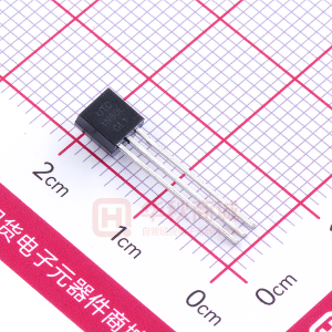
1 1 TO-92
Power MOSFET
DESCRIPTION
The UTC 1N60 is a high voltage MOSFET and is designed to have better characteristics, such as fast switching time, low gate charge, low on-state resistance and have a high rugged avalanche characteristics. This power MOSFET is usually used at high speed switching applications in power supplies, PWM motor controls, high efficient DC to DC converters and bridge circuits. 1
SOT-223
1
TO-220
TO-220F
FEATURES
* RDS(ON) =11.5Ω@VGS = 10V. * Ultra Low gate charge (typical 5.0nC) * Low reverse transfer capacitance (CRSS = typical 3.0 pF) * Fast switching capability * Avalanche energy specified * Improved dv/dt capability, high ruggedness
1 TO-251
1 TO-252
1
SYMBOL
2.Drain
TO-126
1.Gate
3.Source
ORDERING INFORMATION
Ordering Number Package Lead Free Halogen Free 1N60L-x-AA3-R 1N60G-x-AA3-R SOT-223 1N60L-x-T92-B 1N60G-x-T92-B TO-92 1N60L-x-T92-K 1N60G-x-T92-K TO-92 1N60L-x-TA3-T 1N60G-x-TA3-T TO-220 1N60L-x-TF3-T 1N60G-x-TF3-T TO-220F 1N60L-x-TM3-T 1N60G-x-TM3-T TO-251 1N60L-x-TN3-R 1N60G-x-TN3-R TO-252 1N60L-x-TN3-T 1N60G-x-TN3-T TO-252 1N60L-x-T60-K 1N60G-x-T60-K TO-126 Note: Pin Assignment: G: Gate D: Drain S: Source Pin Assignment 1 2 3 G D S G D S G D S G D S G D S G D S G D S G D S G D S Packing Tape Reel Tape Box Bulk Tube Tube Tube Tape Reel Tube Bulk
www.unisonic.com.tw Copyright © 2010 Unisonic Technologies Co., Ltd
1 of 6 QW-R502-052,I
�1N60
ABSOLUTE MAXIMUM RATINGS (TC = 25℃, unless otherwise specified)
PARAMETER SYMBOL 1N60-A 1N60-B
Power MOSFET
RATINGS UNIT 600 V Drain-Source Voltage VDSS 650 V Gate-Source Voltage VGSS ±30 V Avalanche Current (Note 1) IAR 1.2 A Continuous Drain Current ID 1.2 A Pulsed Drain Current (Note 1) IDM 4.8 A Single Pulsed (Note 2) EAS 50 mJ Avalanche Energy Repetitive (Note 1) EAR 4.0 mJ Peak Diode Recovery dv/dt (Note 3) dv/dt 4.5 V/ns SOT-223 1 W TO-251 28 W TO-252 28 W Power Dissipation PD TO-220 40 W TO-220F 21 W TO-92(Ta=25℃) 1 W TO-126 12.5 W Junction Temperature TJ +150 ℃ ℃ Operating Temperature TOPR -55 ~ +150 Storage Temperature TSTG -55 ~ +150 ℃ Note: Absolute maximum ratings are those values beyond which the device could be permanently damaged. Absolute maximum ratings are stress ratings only and functional device operation is not implied.
THERMAL DATA
PARAMETER SOT-223 TO-251 TO-252 TO-220 TO-220F TO-92 TO-126 SOT-223 TO-251 TO-252 TO-220 TO-220F TO-126 SYMBOL RATINGS 150 110 110 62.5 62.5 140 132 14 4.53 4.53 3.13 5.95 10 UNIT
Junction-to-Ambient
θJA
℃/W
Junction-to-Case
θJc
℃/W
UNISONIC TECHNOLOGIES CO., LTD
www.unisonic.com.tw
2 of 6 QW-R502-052,I
�1N60
ELECTRICAL CHARACTERISTICS (TC=25℃, unless otherwise specified.)
PARAMETER OFF CHARACTERISTICS Drain-Source Breakdown Voltage Drain-Source Leakage Current Gate-Source Leakage Current Forward Reverse 1N60-A 1N60-B SYMBOL BVDSS IDSS IGSS TEST CONDITIONS VGS=0V, ID=250μA VDS=600V, VGS=0V VGS=30V, VDS=0V VGS=-30V, VDS=0V
Power MOSFET
MIN TYP MAX UNIT 600 650 10 100 -100 0.4 2.0 4.0 9.3 11.5 120 150 20 25 3.0 4.0 5 25 7 25 5.0 1.0 2.6 20 60 25 60 6.0 V V μA nA nA V/℃ V Ω pF pF pF ns ns ns ns nC nC nC V A A ns μC
Breakdown Voltage Temperature △BVDSS/△TJ ID=250μA Coefficient ON CHARACTERISTICS Gate Threshold Voltage VGS(TH) VDS=VGS, ID=250μA Static Drain-Source On-State Resistance RDS(ON) VGS=10V, ID=0.6A DYNAMIC CHARACTERISTICS Input Capacitance CISS VDS=25V, VGS=0V, f=1MHz Output Capacitance COSS Reverse Transfer Capacitance CRSS SWITCHING CHARACTERISTICS Turn-On Delay Time tD(ON) Turn-On Rise Time tR VDD=300V, ID=1.2A, RG=50Ω (Note 4,5) Turn-Off Delay Time tD(OFF) Turn-Off Fall Time tF Total Gate Charge QG VDS=480V, VGS=10V, ID=1.2A Gate-Source Charge QGS (Note 4,5) Gate-Drain Charge QGD SOURCE-DRAIN DIODE RATINGS AND CHARACTERISTICS Drain-Source Diode Forward Voltage VSD VGS=0V, IS =1.2A Maximum Continuous Drain-Source Diode IS Forward Current Maximum Pulsed Drain-Source Diode ISM Forward Current Reverse Recovery Time tRR VGS=0V, IS=1.2A dIF/dt=100A/μs (Note1) Reverse Recovery Charge QRR Note: 1. Repetitive Rating: Pulse width limited by maximum junction temperature 2. L = 60mH, IAS = 1A, VDD = 50V, RG = 25Ω, Starting TJ = 25°C 3. ISD ≤ 1.2A, di/dt ≤ 200A/μs, VDD ≤ BVDSS, Starting TJ = 25°C 4. Pulse Test: Pulse Width ≤300μs, Duty Cycle≤2% 5. Essentially Independent of Operating Temperature
1.4 1.2 4.8 160 0.3
UNISONIC TECHNOLOGIES CO., LTD
www.unisonic.com.tw
3 of 6 QW-R502-052,I
�1N60
TEST CIRCUITS AND WAVEFORMS
Power MOSFET
D.U.T.
+ VDS -
+ L
RG Driver VGS Same Type as D.U.T. * dv/dt controlled by RG * ISD controlled by pulse period * D.U.T.-Device Under Test VDD
Fig. 1A Peak Diode Recovery dv/dt Test Circuit
VGS (Driver)
Period P.W.
D=
P. W. Period
VGS= 10V
IFM, Body Diode Forward Current ISD (D.U.T.) IRM Body Diode Reverse Current di/dt
Body Diode Recovery dv/dt VDS (D.U.T.) VDD
Body Diode
Forward Voltage Drop
Fig. 1B Peak Diode Recovery dv/dt Waveforms
UNISONIC TECHNOLOGIES CO., LTD
www.unisonic.com.tw
4 of 6 QW-R502-052,I
�1N60
TEST CIRCUITS AND WAVEFORMS (Cont.)
Power MOSFET
Fig. 2A Switching Test Circuit
Fig. 2B Switching Waveforms
Fig. 3A Gate Charge Test Circuit
Fig. 3B Gate Charge Waveform
L VDS BVDSS IAS RD VDD D.U.T. tp tp Time VDD
ID(t)
VDS(t)
10V
Fig. 4A Unclamped Inductive Switching Test Circuit
Fig. 4B Unclamped Inductive Switching Waveforms
UNISONIC TECHNOLOGIES CO., LTD
www.unisonic.com.tw
5 of 6 QW-R502-052,I
�1N60
TYPICAL CHARACTERISTICS
Power MOSFET
Drain Current,ID (mA)
UTC assumes no responsibility for equipment failures that result from using products at values that exceed, even momentarily, rated values (such as maximum ratings, operating condition ranges, or other parameters) listed in products specifications of any and all UTC products described or contained herein. UTC products are not designed for use in life support appliances, devices or systems where malfunction of these products can be reasonably expected to result in personal injury. Reproduction in whole or in part is prohibited without the prior written consent of the copyright owner. The information presented in this document does not form part of any quotation or contract, is believed to be accurate and reliable and may be changed without notice.
Drain Current,ID (µA)
UNISONIC TECHNOLOGIES CO., LTD
www.unisonic.com.tw
Drain Current,ID (µA)
Drain Current, ID (A)
6 of 6 QW-R502-052,I
�