UNISONIC TECHNOLOGIES CO., LTD 2SD1816
NPN EPITAXIAL PLANAR TRANSISTOR
HIGH CURRENT SWITCHIG APPLICATIONS
1
FEATURES
* Low collector-to-emitter saturation voltage * Good linearity of hFE * Small and slim package facilitating compactness of sets. * High fT * Fast switching speed
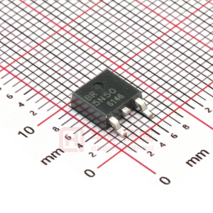
TO-252
1
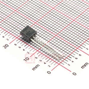
TO-251
*Pb-free plating product number: 2SD1816L
ORDERING INFORMATION
Order Number Normal Lead Free Plating 2SD1816-x-TM3-F-T 2SD1816L-x-TM3-F-T 2SD1816-x-TN3-F-K 2SD1816L-x-TN3-F-K 2SD1816-x-TN3-F-R 2SD1816L-x-TN3-F-R Note: x: Rank, refer to Classification of hFE1.
2SD1816L-x-TM3-F-T (1)Packing Type (2)Pin Assignment (3)Package Type (4)Rank (5)Lead Plating (1) K: Bulk, T: Tube, R: Tape Reel (2) refer to Pin Assignment (3) TM3: TO-251, TN3: TO-252 (4) x: refer to Classification of hFE1 (5) L: Lead Free Plating, Blank: Pb/Sn
Package TO-251 TO-252 TO-252
Pin Assignment 1 2 3 B C E B C E B C E
Packing Tube Bulk Tape Reel
www.unisonic.com.tw Copyright © 2005 Unisonic Technologies Co., Ltd
1 of 4
QW-R209-011,B
�2SD1816
PARAMETER Collector-Base Voltage Collector-Emitter Voltage Emitter-Base Voltage Collector Current Collector Power Dissipation
NPN EPITAXIAL PLANAR TRANSISTOR
ABSOLUTE MAXIMUM RATINGS (Ta =25℃ )
SYMBOL VCBO VCEO VEBO DC PULSE(Note 1) IC PD RATINGS 120 100 6 4 8 1 (TC=25°C) 20 (Note 2) +150 -40 ~ +150 UNIT V V V A A W W °C °C
Junction Temperature TJ Storage Temperature TSTG Note1: Duty=1/2, Pw=20ms Note2: When mounted on a 40×40×0.7mm ceramic board Note3: Absolute maximum ratings are those values beyond which the device could be permanently damaged. Absolute maximum ratings are stress ratings only and functional device operation is not implied.
ELECTRICAL CHARACTERISTICS (Ta=25°C, unless otherwise specified)
PARAMETER Collector Base Breakdown Voltage Collector Emitter Breakdown Voltage Emitter Base Breakdown Voltage Base-Emitter Saturation Voltage Collector-Emitter Saturation Voltage Collector Cut-Off Current Emitter Cut-Off Current DC Current Transfer Ratio Transition Frequency Output Capacitance Turn-on Time Storage Time Fall Time SYMBOL BVCBO BVCEO BVEBO VBE(SAT) VCE(SAT) ICBO IEBO hFE1 hFE2 fT Cob tON tSTG tF TEST CONDITIONS IC =10µA, IE =0 IC =1mA, RB=∞ IE =10µA, IC=0 IC = 2A, IB =0.2A IC = 2A, IB=0.2A VCB = 100 V, IE =0 VEB = 4V, IC=0 VCE = 5V, IC = 0.5A VCE =5V, IC = 3A VCE =10V, IC =0.5A VCB =10V, IE =0A, f =1MHz See test circuit See test circuit See test circuit MIN 120 100 6 TYP MAX UNIT V V V 1.2 V 400 mV 1 µA 1 µA 400 MHz pF ns ns ns
0.9 150
70 40 180 40 100 900 50
CLASSIFICATION of hFE1
RANK RANGE R 100 - 200 S 140 - 280 T 200 - 400 Q 70 -140
TEST CIRCUIT
PW=20 μS Duty Cycle≒1% INPUT
I B1 RB I B2 50 VR + 100µ -5V Ic=10, I B1= -10, IB2=2A Unit (resistance:Ω, capacitance: F) + 470µ 50V OUTPUT
UNISONIC TECHNOLOGIES CO., LTD
www.unisonic.com.tw
2 of 4
QW-R209-011,B
�2SD1816
TYPICAL CHARACTERISTICS
Ic -VCE 5 Colletcor Current, Ic (A) 4 3 2 1 0 80mA 70mA 60mA 100mA mA 90
A 50m A 40m A 30m A 20m
10mA
NPN EPITAXIAL PLANAR TRANSISTOR
Ic -VCE 2.0 1.6 1.2 0.8 0.4 0 4 5 0 10 20
8mA 7mA 6mA 5mA 4mA
ColletcorCurrent, Ic (A)
3mA 2mA 1mA IB=0 30 40 50 Collector to Emitter Voltage,VCE(V)
5mA 2mA I B=0 0 1 2 3 Collector to Emitter Voltage,VCE (V)
Ic -VBE 5
Colletcor Current, Ic(A)
hFE - Ic VCE=5V
DC Current Gain, hFE
1000
7 5 3 2
VCE=5V Ta=75℃ 25℃ -25℃
4 3 2 1 0 0 0.2 0.4 0.6 0.8 Ta=75℃ 25℃ -25℃ 1.0 1.2
100
7 5 3 2
10
7 5 5
0.01
2
3
5
0.1
2
3
5
1.0
23
5
10
Base to Emitter Voltage , VBE (V)
Collector Current,I C(A)
f T -I c
5
Cob - VCB VCE=10V
3
Gain-Bandwidth Product, f T (MHz)
2
Output Capacitance, Cob (pF)
3
2
f=1MHZ
100
7 5 3 2
100
7 5 3 2
7 5
10
2
3
57
0.1
2
3
5
7
1.0
2
3
5
57
1.0
2
3
5
7
10
2
3
5
7 100 2
Colletcor Current Ic (A) ,
Colletcor to Base Voltage, VCB (V)
UNISONIC TECHNOLOGIES CO., LTD
www.unisonic.com.tw
3 of 4
QW-R209-011,B
�2SD1816
TYPICAL CHARACTERISTICS(Cont.)
VCE (SAT) - Ic
5
NPN EPITAXIAL PLANAR TRANSISTOR
VCE( AT) - Ic S 10 Base to Emitter Saturation Voltage, VBE(SAT) (V)
7 5 3 2
Collector to Emitter Saturation Voltage, VCE(SAT) (mV)
3 2
IC/IB=10
IC/I B=10
1000
7 5 3 2
100
7 5 3 2
1.0
7 5 3 2
℃ Ta =-25
25 ℃ 75 ℃
Ta=75℃
℃ 25
℃ -25
5
0.01
2
3
5
0.1
2
3
5
1.0
2
3
5
10
5
0.01 2
3
Collector Current IC (A) ,
1. 2 3 0 Collector Current IC (A) ,
5
0.1
2
3
5
5
10
ASO 10
5 3
PD -Ta 1ms 25
Icp
Ic
DC
D
Collector Dissipation, PD (W)
CollectorCurrent, IC (A)
2
1.0
5 3 2
(T Op a= 25 e rat ℃ ion )
10ms 100ms
20 15 10 5 1 0 No heat sink 0 20 40 60 80 100 120 140 160
C O io n ra t pe
c= (T
0.1
5 3 2
℃ 25 )
0.01
5 2
Tc=25℃ one pulse
3 5
1.0
2
3
5
10
2
3
5
100
2
Colletcor to Emitter Voltage,VCE (V)
Ambient Temperature, , Ta (℃)
UTC assumes no responsibility for equipment failures that result from using products at values that exceed, even momentarily, rated values (such as maximum ratings, operating condition ranges, or other parameters) listed in products specifications of any and all UTC products described or contained herein. UTC products are not designed for use in life support appliances, devices or systems where malfunction of these products can be reasonably expected to result in personal injury. Reproduction in whole or in part is prohibited without the prior written consent of the copyright owner. The information presented in this document does not form part of any quotation or contract, is believed to be accurate and reliable and may be changed without notice.
UNISONIC TECHNOLOGIES CO., LTD
www.unisonic.com.tw
4 of 4
QW-R209-011,B
�