UNISONIC TECHNOLOGIES CO., LTD BU931
NPN POWER DARLINGTON
FEATURES
* High operating junction temperature * High voltage ignition coil driver * Very rugged bipolar technology
NPN SILICON TRANSISTOR
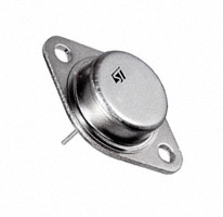
1 TO-3P
INTERNAL SCHEMATIC DIAGRAM
C B (1) (2)
*Pb-free plating product number: BU931L
E
(3)
ORDERING INFORMATION
Order Number Normal Lead Free Plating BU931-T3P-K BU931L-T3P-K Package TO-3P Pin Assignment 1 2 3 B C E Packing Bulk
BU931L-T3P-K
(1)Packing Type (2)Package Type (3)Lead Plating
(1) K: Bulk (2) T3P: TO-3P (3) L: Lead Free Plating, Blank: Pb/Sn
www.unisonic.com.tw Copyright © 2005 Unisonic Technologies Co., Ltd
1 of 5
QW-R214-012,A
�BU931
ABSOLUTE MAXIMUM RATINGS (Ta=25℃)
NPN SILICON TRANSISTOR
PARAMETER SYMBOL RATINGS UNIT Collector-Emitter Voltage (VBE = 0) VCES 500 V Collector-Emitter Voltage (IB = 0) VCEO 400 V Emitter-Base Voltage (IC = 0) VEBO 5 V Collector Current IC 15 A Collector Peak Current ICM 30 A Base Current IB 1 A Base Peak Current IBM 5 A Total Dissipation (Tc = 25 ℃) PD 175 W Junction Temperature TJ +200 ℃ Storage Temperature TSTG -65 ~ +200 ℃ Note: Absolute maximum ratings are those values beyond which the device could be permanently damaged. Absolute maximum ratings are stress ratings only and functional device operation is not implied.
THERMAL DATA
PARAMETER Thermal Resistance Junction-Case Max SYMBOL θJC RATING 1.1 UNIT ℃/W
ELECTRICAL CHARACTERISTICS
PARAMETER Collector Cut-off Current (IB = 0) Emitter Cut-off Current (IC = 0) Collector-Emitter Saturation Voltage(Note) SYMBOL ICEO IEBO VCE(SAT) TEST CONDITIONS VCE = 450 V VCE = 450 V, TJ = 125 ℃ VEB = 5 V IC = 7 A, IB = 70 mA IC = 8 A, IB = 100 mA IC = 10 A, IB = 250 mA IC = 7 A, IB = 70 mA IC = 8 A, IB = 100 mA IC = 10 A, IB = 250 mA IC = 5 A, VCE = 10 V IF = 10 A VCC = 24 V, Vclamp = 400 V L = 7 mH VCC = 12 V, Vclamp = 300 V L = 7 mH IC = 7 A, IB = 70 mA VBE = 0, RBE = 47Ω MIN TYP MAX UNIT 100 µA 0.5 mA 20 mA 1.6 V 1.8 1.8 2.2 2.4 2.5 300 2.5 8 15 0.5 V A µs µs V V V V V
Base-Emitter Saturation Voltage(Note) DC Current Gain Diode Forward Voltage Functional Test
VBE(SAT) hFE VF
Inductive Load Storage Time / Fall Time
tS tF
Note: Pulsed: Pulse duration = 300 µs, duty cycle 1.5 %
UNISONIC TECHNOLOGIES CO., LTD
www.unisonic.com.tw
2 of 5
QW-R214-012,A
�BU931
TEST CIRCUITS
NPN SILICON TRANSISTOR
24V L=7mH VZ Driver and current limiting circuit 100Ω
VD
12V
7mH T.U.T 0.22µF VIN T.U.T 47Ω 0.2Ω Vclamp
Functional Test Circuit
Switching Time Test Circuit
UNISONIC TECHNOLOGIES CO., LTD
www.unisonic.com.tw
3 of 5
QW-R214-012,A
�BU931
TYPICAL CHARACTERISTICS
Collector Emitter Saturation Voltage vs. Collector Current Collector-Emitter Saturation Voltage, VCE(SAT)(V) Collector-Emitter Saturation Voltage, VCE(SAT) (V) hFE=50 3
NPN SILICON TRANSISTOR
Collector Emitter Saturation Voltage vs. Collector Current hFE=100 3
2 -40℃ 25℃
2 25℃ 1 -40℃ 125℃ 0 1 2 4 6
1
125℃ 0 1 2 4 6
Collector Current IC (A) ,
Collector Current, I C (A)
Base Emitter Saturation Voltage vs. Collector Current
Base Emitter Saturation Voltage vs. Collector Current
Base-Emitter Saturation Voltage, VBE(SAT) (V)
Base-Emitter Saturation Voltage, VBE(SAT)(V)
h FE=50 3
hFE=100 3
2
-40℃ 25℃
2
-40℃ 25℃
1
125℃
1
125℃
0
1
2
4
6
0
1
2
4
6
Collector Current IC (A) ,
DC Current Gain vs. Collector Current
8 6
Collector Current, IC (A)
VCE=2V
DC Current Gain, hFE
4
2
25℃
10
2 8 6 4
2
10 -1 10
2
4
6
8
1
2
4
68
Collector Current, IC (A)
UNISONIC TECHNOLOGIES CO., LTD
www.unisonic.com.tw
4 of 5
QW-R214-012,A
�BU931
NPN SILICON TRANSISTOR
UTC assumes no responsibility for equipment failures that result from using products at values that exceed, even momentarily, rated values (such as maximum ratings, operating condition ranges, or other parameters) listed in products specifications of any and all UTC products described or contained herein. UTC products are not designed for use in life support appliances, devices or systems where malfunction of these products can be reasonably expected to result in personal injury. Reproduction in whole or in part is prohibited without the prior written consent of the copyright owner. The information presented in this document does not form part of any quotation or contract, is believed to be accurate and reliable and may be changed without notice.
UNISONIC TECHNOLOGIES CO., LTD
www.unisonic.com.tw
5 of 5
QW-R214-012,A
�
很抱歉,暂时无法提供与“BU931”相匹配的价格&库存,您可以联系我们找货
免费人工找货