UNISONIC TECHNOLOGIES CO., LTD
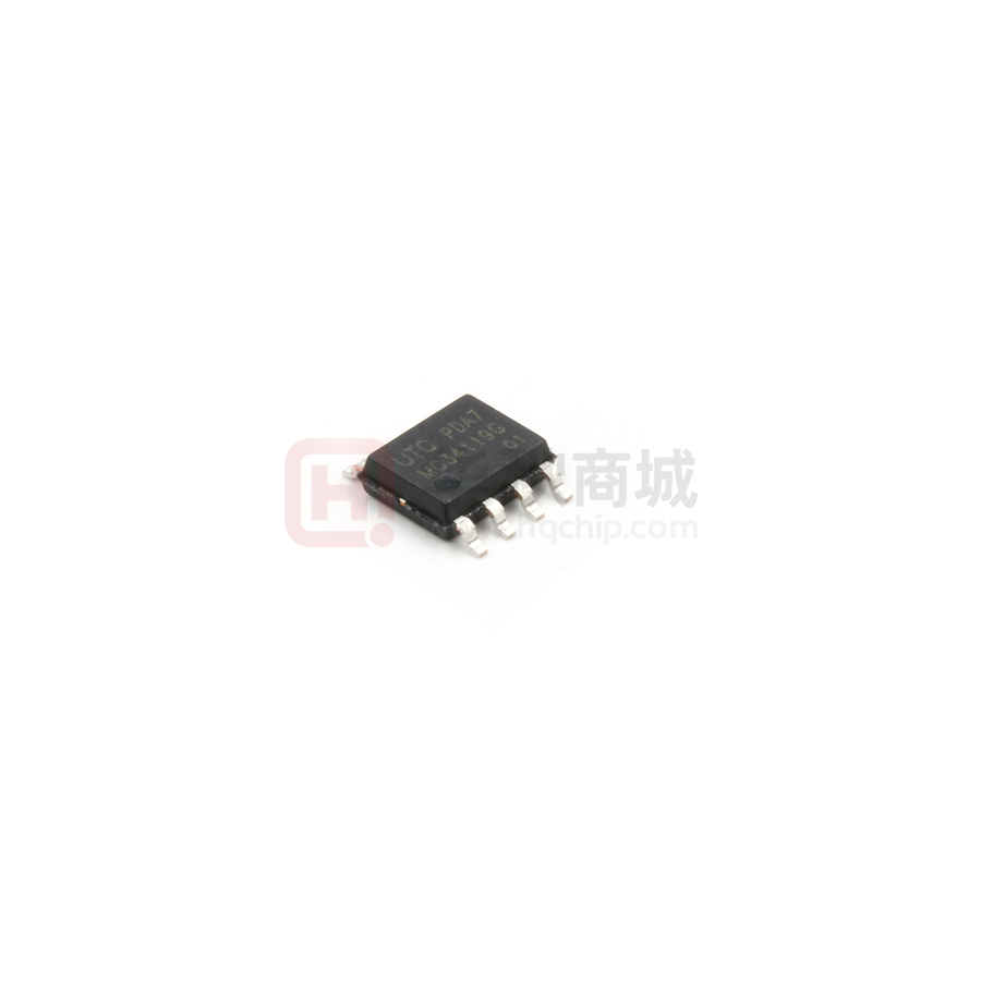
MC34119
LINEAR INTEGRATED CIRCUIT
LOW POWER AUDIO
AMPLIFIER
DESCRIPTION
The UTC MC34119 is a low power audio amplifier IC intended for
the telephone applications, such as in speakerphones. It provides
differential speaker outputs to maximize output swing at low supply
voltages. Coupling capacitor to the speaker is not required. Open
loop gain is 80dB, and the closed loop gain is set with two external
resistors. The Mute pin permits powering down and/or muting the
input signal.
FEATURES
* Wide operating supply voltage: VCC=2V~16V
* Low quiescent supply current (ICC=2.7mA, typ)
* Medium power output over 250mW at VCC=6V,
RL=32Ω, THD<10%
* Load impedance range (8Ω~100Ω)
* Low total harmonic distortion (0.5% typ)
* Mute function (ICC=65μA, typ)
* Minimum number of external parts required
ORDERING INFORMATION
Ordering Number
Lead Free
MC34119L-D08-T
-
Halogen Free
MC34119G-D08-T
MC34119G-S08-R
MC34119G-P08-R
MC34119G-K08-3030-R
MC34119L-D08-T
(1)Packing Type
(2)Package Type
(3)Green Package
www.unisonic.com.tw
Copyright © 2016 Unisonic Technologies Co., Ltd
Package
Packing
DIP-8
SOP-8
TSSOP-8
DFN-8(3×3)
Tube
Tape Reel
Tape Reel
Tape Reel
(1) T: Tube, R: Tape Reel
(2) D08: DIP-8, S08: SOP-8, P08: TSSOP-8
K08-3030: DFN-8(3×3)
(3) L: Lead Free, G: Halogen Free and Lead Free
1 of 8
QW-R107-038.J
�MC34119
LINEAR INTEGRATED CIRCUIT
MARKING
DIP-8
SOP-8
TSSOP-8
DFN-8(3×3)
UTC
MC34119G
Date Code
Lot Code
PIN CONFIGURATION
PIN DESCRIPTION
PIN NO.
1
2
3
4
5
6
7
8
PIN NAME
DESCRIPTION
This pin can be used to power down the IC to converse power, or for muting, or both. When
Mute
at a logic “LOW” (less than 0.8V), the IC is enabled for normal operation. When at a logic
“HIGH” (2V to VCC), the IC is disabled. If Mute is open, that is equivalent to a logic “LOW”.
Ripple
A capacitor at this pin increase power supply rejection, and affects turn-on time. This pin
Rejection can be left open if the capacitor at pin 3 is sufficient.
Analog Ground for the amplifiers. A 1μF capacitor at this pin (with a 5μF capacitor at pin 2)
Input(+) provides 52dB( typ) of power supply rejection. Turn-on time of the circuit is affected by the
capacitor on this pin. This pin can be used as an alternative input.
Amplifier input. The input capacitor and resistor set low frequency roll-off and input
Input(-)
impedance. The feedback resistor is connected between this pin and output 1.
Output 1 Amplifier output 1. The DC level is about (VCC~0.7V)/2.
VCC
DC supply voltage is applied to this pin (VCC=2~16V).
GND
Ground pin.
Amplifier output 2. This signal is equal in amplitude, but 180°out of phase with that output 1,
Output 2
the DC level is about (Vcc~0.7V)/2.
UNISONIC TECHNOLOGIES CO., LTD
www.unisonic.com.tw
2 of 8
QW-R107-038.J
�MC34119
LINEAR INTEGRATED CIRCUIT
BLOCK DIAGRAM
IN-
4
Amp 1
IN+
VCC
5
OUT1
8
OUT2
1
MUTE
3
6
Bias
2
7
RR
GND
UNISONIC TECHNOLOGIES CO., LTD
www.unisonic.com.tw
3 of 8
QW-R107-038.J
�MC34119
LINEAR INTEGRATED CIRCUIT
ABSOLUTE MAXIMUM RATINGS (TA=25C, unless otherwise specified)
PARAMETER
SYMBOL
RATINGS
UNIT
Supply Voltage
VCC
-1 ~ +18
V
±250
Output Current
IOUT
mA
Maximum Input, Ripple Rejection, Mute Pin Voltage
VIN
-1 ~ +1
V
Applied Output Voltage (Output Pin When Disabled)
VOUT
-1 ~ +1
V
Junction Temperature
TJ
+125
C
Operating Temperature
TOPR
-20 ~ +85
C
Storage Temperature
TSTG
-40 ~ +150
C
Note: Absolute maximum ratings are those values beyond which the device could be permanently damaged.
Absolute maximum ratings are stress ratings only and functional device operation is not implied.
RECOMMENDED OPERATION CONDITIONS (TA=25C, unless otherwise specified)
PARAMETER
Supply Voltage
Load Impedance
Peak Load Current
Differential Gain (5KHz Bandwidth)
Voltage at Mute
Ambient Temperature
SYMBOL
VCC
ZL
IL(PEAK)
GV
VI(MUTE)
TA
RATINGS
2~16
8~100
±200
0~46
0~VCC
-20~+70
UNIT
V
Ω
mA
dB
V
C
ELECTRICAL CHARACTERISTICS (VCC=6V, TA=25C, unless otherwise specified)
PARAMETER
DC PARAMETER
SYMBOL
Operating Current
Output Voltage
ICC
VOUT
Output Offset Voltage
Output High Level
Output Low Level
Input Bias Current
VO(OFF)
VOH
VOL
II(BIAS)
Equivalent Resistance
REQ
AC PARAMETER
Open Loop Gain of Amp. 1
Open Loop Gain of Amp. 2
GV1
GV2
Output Power
POUT
Total Harmonic Distortion
(f=1KHz)
THD
Gain Bandwidth Product
GBW
Power Supply Rejection
(VCC=6V, VCC=3V)
RR
Muting
GV(MUTE)
TEST CONDITIONS
VCC=3V, Mute=0.8V
VCC=16V, Mute=0.8V
VCC=3V, Mute=2V
RL=16Ω, R1=75KΩ, VCC=3V
RL=16Ω, R1=75KΩ, VCC=6V
RL=16Ω, R1=75KΩ, VCC=12V
VCC=6V, RF=75KΩ,RL=32Ω
2V
很抱歉,暂时无法提供与“MC34119G-SO8-R”相匹配的价格&库存,您可以联系我们找货
免费人工找货- 国内价格
- 5+0.53904
- 50+0.48882
- 500+0.43860
- 1000+0.38839
- 2500+0.36495
- 5000+0.34486
- 国内价格
- 1+0.88480
- 10+0.81680
- 100+0.59890
- 1000+0.54450
- 国内价格
- 1+0.74250
- 100+0.49500
- 1250+0.44990
- 2500+0.41690
