UNISONIC TECHNOLOGIES CO., LTD
TDA7052A
LINEAR INTEGRATED CIRCUIT
1W BTL MONO AUDIO
AMPLIFIER WITH DC VOLUME
CONTROL
DIP-8
DESCRIPTION
The UTC TDA7052A is mono BTL output amplifier with DC
volume control. It is designed for use in TV and monitors,
additionally it is suitable for portable recorders and radios.
In the IC, a Missing Current Limiter (MCL) is built-in. This
function is activated when the difference of current between the
OUT+ and OUT- exceed 100mA (typical 300mA). This level of
100mA suit for headphone applications (single-ended).
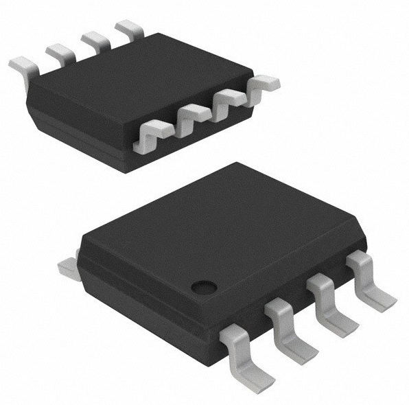
SOP-8
FEATURES
* Low power consumption
* DC volume control
* Mute mode
* No switch-on and off clicks
* Short-circuit proof
* Good overall stability
* Low HF radiation
* Few external components
* Thermal protection
* ESD protected on all pins
* Missing Current Limiter (MCL)
ORDERING INFORMATION
Ordering Number
Lead Free
Halogen Free
TDA7052AL-D08-T
TDA7052AG-D08-T
TDA7052AL-S08-T
TDA7052AG-S08-T
TDA7052AL-S08-R
TDA7052AG-S08-R
Package
Packing
DIP-8
SOP-8
SOP-8
Tube
Tube
Tape Reel
MARKING
www.unisonic.com.tw
Copyright © 2017 Unisonic Technologies Co., Ltd
1 of 5
QW-R107-075.B
�TDA7052A
LINEAR INTEGRATED CIRCUIT
PIN CONFIGURATION
PIN DESCRIPTION
PIN NO.
1
2
3
4
5
6
7
8
PIN NAME
VP
IN+
GND1
VC
OUT+
GND2
NC
OUT-
DESCRIPTION
Power Supply
Signal Input Terminal
Signal Ground
DC Volume Control Terminal
Non-inverted Output Terminal
Power Ground
Not Connected
Inverted Output Terminal
BLOCK DIAGRAM
VP
1
Thermal Protection/MCL
I+i
5
Non-inverted
Output
Signal Input 2
+
DC Volume
4
Control
-
Vref
+
STABILIZER
3
Signal
Ground
I-i
7
n.c.
UNISONIC TECHNOLOGIES CO., LTD
www.unisonic.com.tw
8 Inverted Output
6
Power
Ground
2 of 5
QW-R107-075.B
�TDA7052A
LINEAR INTEGRATED CIRCUIT
ABSOLUTE MAXIMUM RATING
PARAMETER
Supply Voltage Range
Input Voltage Pin 2
Input Voltage Pin 4
Repetitive Peak Output Current
Non-Repetitive Peak Output Current
Short-Circuit Time
RATINGS
UNIT
18
V
8
V
8
V
1.25
A
1.5
A
1
hr
DIP-8
1.25
W
Total Power Dissipation (TA≤25%)
PD
SOP-8
0.8
W
Operating Ambient Temperature Range
TA
-40 ~ +85
°C
Junction Temperature
TJ
+150
°C
Storage Temperature Range
TSTG
-55 ~ +150
°C
Note: Absolute maximum ratings are those values beyond which the device could be permanently damaged.
Absolute maximum ratings are stress ratings only and functional device operation is not implied.
SYMBOL
VP
V2
V4
IORM
IOSM
TSC
ELECTRICAL CHARACTERISTICS
VP=6V, Tamb=25°C, f=1kHz; RL=8Ω, unless otherwise specified.
PARAMETER
SYMBOL
TEST CONDITIONS
MIN
TYP
MAX UNIT
Power Supply Voltage Range
VP
4.5
18
V
Total Quiescent Current
IP
VP=6V, RL=∞, Note 1
7
12
mA
DC Volume Control
Gain Control Range
φ
75
80
dB
Control Current
I4
V4=0.4V
70
80
µA
Characteristics In Mute Position
Output Voltage In Mute Position
VO
V4≤0.3V, VI=600mV
30
µV
Characteristics In Minimum Gain, V4=0.5V
Voltage Gain
GV
-44
dB
Noise Output Voltage (RMS value)
VNO(RMS) Note 2
20
30
µV
Characteristics In Maximum Gain, V4=1.4V
Output Power
PO
THD=10%
1.0
1.1
W
Total Harmonic Distortion
THD
PO=0.5W
0.3
1
%
Voltage Gain
GV
34.5
35.5
36.5
dB
Input Signal Handling
VI
V4=0.8V, THD
很抱歉,暂时无法提供与“TDA7052AG-S08-R”相匹配的价格&库存,您可以联系我们找货
免费人工找货- 国内价格
- 1+1.93610
- 10+1.43210
- 100+1.22750
- 1000+1.02290
- 国内价格
- 1+1.24320
- 100+0.95424
- 1250+0.80864
- 2500+0.74928
- 国内价格
- 1+1.60210
- 10+1.31810
- 30+1.08440
- 100+0.97630
- 300+0.89000
- 5000+0.83800
