UNISONIC TECHNOLOGIES CO., LTD UT3N06
Preliminary Power MOSFET
N-CHANNEL ENHANCEMENT MODE POWER MOSFET
DESCRIPTION
The UTC UT3N06 is an N-channel POWER MOSFET providing very low on-resistance. It has high efficiency and perfect cost-effectiveness. It can be generally applied in the commercial and industrial fields.
FEATURES
* Simple drive requirement * Halogen Free
SYMBOL
(3) D
(2) G
(1) S
ORDERING INFORMATION
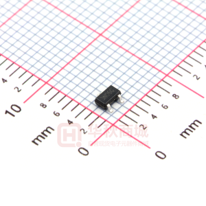
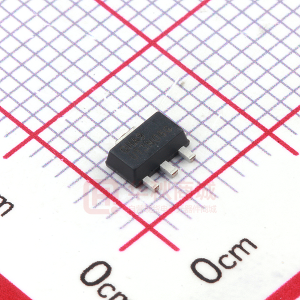
Ordering Number UT3N06G-AE3-R Package SOT-23 1 S Pin Assignment 2 3 G D Packing Tape Reel
MARKING
3N06G
www.unisonic.com.tw Copyright © 2009 Unisonic Technologies Co., Ltd
1 of 3
QW-R502-366.a
�UT3N06
Preliminary
Power MOSFET
ABSOLUTE MAXIMUM RATINGS
PARAMETER SYMBOL RATINGS UNIT Drain-Source Voltage VDSS 60 V Gate-Source Voltage VGSS ±20 V Continuous Drain Current ID 3.0 A (VGS=4.5V, Ta= 25°C) (Note 2) Pulsed Drain Current (Note 3.4) IDM 10 A Power Dissipation (Ta= 25°C) PD 1.38 W Junction Temperature TJ +150 °C Storage Temperature TSTG -55 ~ +150 °C Note: 1. Absolute maximum ratings are those values beyond which the device could be permanently damaged. Absolute maximum ratings are stress ratings only and functional device operation is not implied. 2. Surface mounted on 1 in2 copper pad of FR4 board; 270°C/W when mounted on min. copper pad. 3. Pulse width limited by TJ(MAX) 4. Pulse width ≤300μs, duty cycle≤2%.
THERMAL DATA
PARAMETER SYMBOL MIN TYP MAX Junction to Ambient (Note) θJA 90 Note: Surface mounted on 1 in2 copper pad of FR4 board; 270°C/W when mounted on min. copper pad. UNIT °C/W
ELECTRICAL CHARACTERISTICS (TJ = 25°C, unless otherwise specified)
PARAMETER OFF CHARACTERISTICS Drain-Source Breakdown Voltage Breakdown Voltage Temperature Coefficient Drain-Source Leakage Current Gate-Source Leakage Current ON CHARACTERISTICS Gate Threshold Voltage Drain to Source On-state Resistance SYMBOL BVDSS ΔBVDSS ΔTJ IDSS IGSS VGS(TH) RDS(ON) TEST CONDITIONS VGS =0V, ID =250µA Reference to 25°C, ID=1mA VDS =60V,VGS =0V VGS =±20V VDS =VGS, ID =250µA VGS =10V, ID =3A VGS =4.5V, ID =2A 1.0 MIN 60 0.05 10 ±100 3.0 90 120 490 55 40 6 5 16 3 6 1.6 3 780 TYP MAX UNIT V V/°C µA nA V mΩ mΩ pF pF pF ns ns ns ns nC nC nC V ns nC
DYNAMIC PARAMETERS Input Capacitance CISS Output Capacitance COSS VDS=25V,VGS=0V,f =1.0MHz Reverse Transfer Capacitance CRSS SWITCHING PARAMETERS Turn-ON Delay Time (Note) tD(ON) Turn-ON Rise Time tR VGS=10V, VDS=30V, ID=1A, Turn-OFF Delay Time tD(OFF) RD =30Ω, RG =3.3Ω Turn-OFF Fall-Time tF Total Gate Charge (Note) QG VGS =4.5V, VDS =48V, ID =3A Gate Source Charge QGS Gate Drain Charge QGD SOURCE- DRAIN DIODE RATINGS AND CHARACTERISTICS Drain-Source Diode Forward Voltage (Note) VSD IS =1.2A, VGS =0V Reverse Recovery Time tRR IS=3A,VGS=0V,dI/dt=100A/µs Reverse Recovery Charge QRR Note: Pulse width ≤300μs, duty cycle≤2%.
10
1.2 25 26
UNISONIC TECHNOLOGIES CO., LTD
www.unisonic.com.tw
2 of 3
QW-R502-366.a
�UT3N06
TEST WAVEFORMS
Preliminary
Power MOSFET
VG
4.5V
QG
QGS
QGD
Charge Switching Time Waveform Gate Charge Waveform
Q
U TC assumes no responsibility for equipment failures that result from using products at values that exceed, even momentarily, rated values (such as maximum ratings, operating condition ranges, or other parameters) listed in products specifications of any and all UTC products described or contained herein. UTC products are not designed for use in life support appliances, devices or systems where malfunction of these products can be reasonably expected to result in personal injury. Reproduction in whole or in part is prohibited without the prior written consent of the copyright owner. The information presented in this document does not form part of any quotation or contract, is believed to be accurate and reliable and may be changed without notice.
UNISONIC TECHNOLOGIES CO., LTD
www.unisonic.com.tw
3 of 3
QW-R502-366.a
�
很抱歉,暂时无法提供与“UT3N06”相匹配的价格&库存,您可以联系我们找货
免费人工找货- 国内价格
- 10+0.37361
- 100+0.29376
- 600+0.28935
- 1200+0.28067
- 3000+0.26804
- 国内价格
- 5+0.57693
- 50+0.45305
- 150+0.39122
- 国内价格
- 10+0.3751
- 100+0.3509
- 500+0.3267
- 2000+0.2904
- 5000+0.2783
- 10000+0.27104