UNISONIC TECHNOLOGIES CO., LTD
UTRS485
Preliminary
CMOS IC
FAIL-SAFE, 2.5MBPS, RS-485 /
RS-422 TRANSCEIVERS WITH
±15KV ESD-PROTECTED
DESCRIPTION
The UTC UTRS485 is a half-duplex transceiver designed for
RS-485 data bus network, which contains one transmitter and one
receiver. The UTC UTRS485 features a fail-safe receiver, which
guarantees the receiver to output high when the receiver inputs are
open, short or idle.
The UTC UTRS485 also features a hot-swap glitch free protection
circuits which guarantee outputs of both the transmitter and the
receiver in a high impedance state during the power up period. So that
the large short current from power to ground will be disable by glitch
free function, which will save the power and enhance the efficiency of
the power up.
The UTC UTRS485 is optimized for signal rates up to 2.5Mbps
with differential voltage of 2.3V. The UTC UTRS485 also has the
thermal shutdown function when the temperature is over 150℃ and
the protection of the current limitation in the transmitter to protect the
itself from the damage by the system-fault conditions during normal
operation.
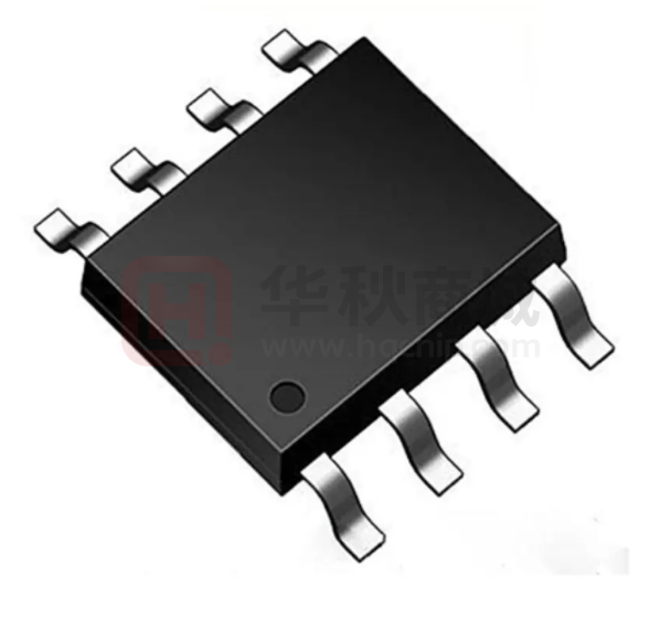
SOP-8
FEATURES
* Meet the requirements of the EIA/TIA-485 standards.
* 5.0V single power supply.
* True fail-safe receiver while maintaining EIA/TIA-485 compatibility.
* Hot-Swap glitch free protection on control inputs.
* Up to 256 transceivers on the bus.
* Driver short circuit current limit.
* Thermal shutdown for overload protection.
ORDERING INFORMATION
Ordering Number
UTRS485G-S08-R
Package
SOP-8
Packing
Tape Reel
UTRS485G-S08-R
(1)Packing Type
(1) R: Tape Reel
(2)Package Type
(2) S08: SOP-8
(3)Green Package
(3) G: Halogen Free and Lead Free
www.unisonic.com.tw
Copyright © 2015 Unisonic Technologies Co., Ltd
1 of 8
QW-R113-011.c
�UTRS485
Preliminary
MARKING
PIN CONFIGURATION
RO 1
8 VCC
RE
2
7 B
DE 3
6 A
DI 4
CMOS IC
5 GND
PIN DESCRIPTION
PIN NO.
1
PIN NAME
RO
2
RE
3
DE
4
DI
5
6
7
8
GND
A
B
VCC
DESCRIPTION
Receiver output: if A>B by 200mV, RO will be high; if A
很抱歉,暂时无法提供与“UTRS485G-S08-R”相匹配的价格&库存,您可以联系我们找货
免费人工找货- 国内价格
- 1+1.40800
- 100+1.07910
- 1250+0.93830
- 2500+0.88550
- 国内价格
- 5+1.91074
- 50+1.48490
- 150+1.30248
- 500+1.07471
- 2500+0.97341
- 5000+0.91250
