FX-402-EDE-KC

FX-402-EDE-KC

  • 厂商:

    VECTRON

  • 封装:

  • 描述:

    FX-402-EDE-KC - Low Jitter Frequency Translator - Vectron International, Inc

  • 详情介绍
  • 数据手册
  • 价格&库存
FX-402-EDE-KC 数据手册
FX-402 Low Jitter Frequency Translator Previous Part Number FX-427 FX-402 Description The FX-402 is a precision quartz-based frequency translator used to translate 1 to 4 selected input clocks as low as 8 kHz to an integer multiple as high as 850 MHz. The FX-402’s superior jitter performance is achieved through the filtering action of the onboard voltage-controlled SAW oscillator (VCSO) and integrated loop filter. Two low-jitter outputs are provided. Monitoring and control functionality are also standard features. Features • • • • • • • • • Quartz-based PLL for Ultra-Low Jitter Frequency Translation up to 850 MHz Accepts 4 externally-muxed clock inputs LVCMOS/LVDS/LVPECL Inputs Compatible Differential LVPECL Outputs Lock Detect Output Disable 20.3 x 13.7 x 5.1 mm surface mount package Compliant to EC RoHS Directive • • • • • • Applications Wireless Infrastructure 802.16 BTS 10 Gigabit FC 10GbE LAN / WAN OADM and IP Routers Test Equipment Block Diagram VCC (14) FIN1 FIN2 FIN3 FIN4 FIN (13) LD (7) Phase Detector & LD VMON (5) Loop Filter VCSO (8) FOUT1 (9) CFOUT1 ÷ μ Controller SEL0 (1) SEL1 (2) ÷ ÷ (10) FOUT2 (11) CFOUT2 GND (3, 12) OD (6) Figure 1. Functional block diagram Page 1 of 8 Vectron International • 267 Lowell Road, Hudson, NH 03051 • Tel: 1-88-VECTRON-1 • http://www.vectron.com Rev: 8/13/2009 Performance Specifications Table 1. Electrical Performance Parameter Frequency Input Frequency Capture Range Output Frequency - Primary Output Frequency - Secondary Supply Voltage 2, 3 Current (No Load)3 Input Signal LVCMOS LVDS 2, 3, 7 LVPECL Differential Output (Options F and P) 2, 3, 4, 5 Common Mode Output Voltage DC Output High Voltage DC Output Low Voltage Peak to Peak Output Voltage Rise TIme Fall Time Symmetry SSB Phase Noise, Fout = 155.52/622.08 10Hz Offset 100Hz Offset 1kHz Offset 10kHz Offset 100kHz Offfset 1 MHz Offset 10 MHz Offset Jitter Generation 5, 6 155.52 MHz (12kHz - 20MHz BW) 622.08 MHz (12kHz - 20 MHz BW) Operating Temperature (Options C of F) 1 ,3 5, 6 1, 2, 3 Symbol FIN APR FOUT1 FOUT2 VCC ICC FIN FIN FIN VOCM VOH VOL VP-P tR tF SYM Φn Φn Φn Φn Φn Φn Φn ΦJ ΦJ TOP Min 0.008 ±40 500 125 3.13 Typical Maximum 400 850 850 Units MHz ppm MHz MHz V mA 3.3 140 LVCMOS LVDS LVPECL 3.46 180 VCC-1.5 VCC-1.085 VCC-1.830 45 VCC-1.3 VCC-0.950 VCC-1.7 700 0.5 0.5 50 -64/-27 -95/-55 -123/-123 -143/-110 -146/-130 -146/-146 -146/-146 0.30 0.12 0 to 70 or -40 to 85 VCC-1.1 VCC-0.880 VCC-1.620 55 V V V mV p-p ns ns % dBc/Hz dBc/Hz dBc/Hz dBc/Hz dBc/Hz dBc/Hz dBc/Hz ps RMS ps RMS 0C 1. See Standard Frequencies and Ordering Information. 2. Parameters are tested with production test circuit below (Fig 2). 3. Parameters are tested at ambient temperature with test limits guard banded for specified operating temperature. 4. Measured from 20% to 80% of a full output swing (Fig 3). 5. Not tested in production, guaranteed by design, verified at qualification. 6. The FX-402 phase noise and jitter performance can be optimized for specific applications. Please consult with Vectron’s Application Engineers for more information. 7. LVCMOS input signal levels are valid for input frequencies < 100 MHz. Page 2 of 8 Vectron International • 267 Lowell Road, Hudson, NH 03051 • Tel: 1-88-VECTRON-1 • http://www.vectron.com Rev: 8/13/2009 Absolute Maximum Ratings Stresses in excess of the absolute maximum ratings can permanently damage the device. Functional operation is not implied at these or any other conditions in excess of conditions represented in the operational sections of this data sheet. Exposure to absolute maximum ratings for extended periods may adversely affect device reliability. Table 2. Absolute Maximum Ratings Parameter Power Supply Storage Temperature Soldering Tewmp/TIme Symbol VDD TSTR TLS Ratings 6 -55 to 125 260/40 Unit V 0C 0C/sec Reliability The FX-402 is capable of meeting the following qualification tests Table 3. Environmental Compliance Parameter Mechanical Shock Mechanical Vibration Solderability Gross and Fine Leak Resistance to Solvents Conditions MIL-STD-883, Method 2002 MIL-STD-883, Method 2007 MIL-STD-883, Method 2003 MIL-STD-883, Method 1014 MIL-STD-883, Method 2016 Handling Precautions Although ESD protection circuitrry has been designed into the the FX-402, proper precautions should be taken when handling and mounting. VI employs a human body model and a charged-device model (CDM) for ESD susceptibility testing and design protection evaluation. ESD thresholds are dependent on the circuit parameters used to define the model. Although no industry wide standard has been adopted for the CDM, a standard HBM of resistance=1.5Kohms and capacitance = 100pF is widely used and therefore can be used for comparison purposes Table 4. Predicted ESD R$atings Model Human Body Model Charged Device Model Minimum 500 V 500 V Conditions MIL-STD 883, Method 3015 JEDEC, JESD22-C101 Page 3 of 8 Vectron International • 267 Lowell Road, Hudson, NH 03051 • Tel: 1-88-VECTRON-1 • http://www.vectron.com Rev: 8/13/2009 Reflow Profile Table 5. Reflow Profile (IPC/JEDEC J-STD-020C) Parameter PreHeat Time Ramp Up Time Above 217 0C Time To Peak Temperature Time At 260 0C Ramp Down Symbol tS RUP tL tAMB-P tP RDN Value 60 sec Min, 180 sec Max 3 0C/sec Max 60 sec Min, 150 sec Max 480 sec Max 20 sec Min, 40 sec Max 6 0C/sec Max The FX-402 is qualified to meet the JEDEC standard for Pb-Free assembly. The temperatures and time intervals listed are based on the Pb-Free small body requirements. The temperatures refer to the topside of the package, measured on the package body surface. The FX-402 should not be subjected to a wash process that will immerse it in solvents. NO CLEAN is the recommended procedure. The FX-402 has been designed for pick and place reflow soldering. The FX-402 may be reflowed once and should not be reflowed in the inverted position. Figure 4. Suggested IR Profile Tape and Reel Table 6. Tape and Reel Information Tape Dimensions (mm) W F Do Po P1 A B Reel Dimensions (mm) C D N W1 W2 #/Reel 32 14.2 1.5 4 20 330 1.5 13 20.2 100 44.4 50.4 200 Figure 5. Tape and Reel Page 4 of 8 Vectron International • 267 Lowell Road, Hudson, NH 03051 • Tel: 1-88-VECTRON-1 • http://www.vectron.com Rev: 8/13/2009 Pin Configuration Figure 6. Pin Configuration Table 7. Pin Functions Pin # 1 2 3 4 5 VMON O Symbol SEL0 SEL1 GND I I GND I/O Level LVCMOS LVCOMS Supply Frequency Select - see table 3 Frequency Select – see table 3 Case and Electrical Ground Not present Function VCXO Control Voltage Monitor Under locked conditions VMON should be > 0.3V and
FX-402-EDE-KC
物料型号: - 型号为FX-402,之前的部分型号为FX-427。

器件简介: - FX-402是一款基于精准石英的频率转换器,可以将1至4个选择的输入时钟信号从低至8 kHz的频率转换为高达850 MHz的整数倍。FX-402通过板上电压控制的表面声波振荡器(VCSO)和集成的环路滤波器实现卓越的抖动性能。提供两个低抖动输出,并具备监控和控制功能。

引脚分配: - SELO(1号引脚):频率选择,LVCMOS电平。 - SEL1(2号引脚):频率选择,LVCMOS电平。 - GND(3号和12号引脚):供电和电气地。 - VMON(5号引脚):VXCO控制电压监控,在锁定条件下VMON应大于0.3V且小于3.0V。 - OD(6号引脚):输出禁用,禁用=逻辑"1",启用=逻辑"0"或不连接,LVCMOS电平。 - LD(7号引脚):锁定检测,锁定=逻辑"1",失锁=逻辑"0",LVCMOS电平。 - FOUT1(8号引脚):频率输出-主输出,LVPECL电平。 - CFOUT1(9号引脚):互补频率输出-主输出,LVPECL电平。 - FOUT2(10号引脚):降低的VCSO/CXO输出或禁用,LVPECL电平。 - CFOUT2(11号引脚):降低的VCSO/VCXO互补输出或禁用,LVPECL电平。 - FIN(13号引脚):输入频率,交流耦合,LVCMOS或LVPECL电平。 - VCC(14号引脚):供电电压(3.3V±5%)。

参数特性: - 输入频率捕获范围:0.008 MHz至850 MHz。 - 电源电压:3.13 V至3.46 V。 - 工作温度:0至70°C或-40至85°C。 - 供电电流(无负载):3.3 mA至140 mA。

功能详解: - 基于石英的PLL,用于超低抖动。 - 频率转换高达850 MHz。 - 接受4个外部多路复用时钟输入。 - LVCMOS/LVDS/LVPECL输入兼容。 - 差分LVPECL输出。 - 锁定检测、输出禁用。 - 
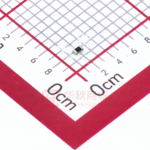
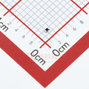
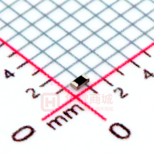
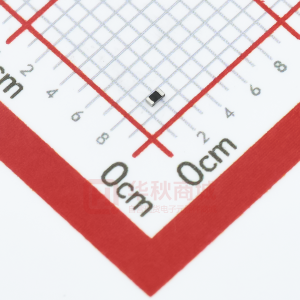
20.3 x 13.7 x 5.1 mm表面贴装封装,符合EC RoHS指令。

应用信息: - 无线基础设施、802.16 BTS、10 Gigabit FC、10GbE LAN/WAN、OADM和IP路由器、测试设备。

封装信息: - 20.3 x 13.7 x 5.1 mm表面贴装封装。
FX-402-EDE-KC 价格&库存

很抱歉,暂时无法提供与“FX-402-EDE-KC”相匹配的价格&库存,您可以联系我们找货

免费人工找货
CR0402-FX-2701GLF
    •  国内价格
    • 50+0.04661
    • 500+0.04238
    • 5000+0.03673
    • 30000+0.03531
    • 90000+0.0339

    库存:45

    CR0402-FX-1603GLF
    •  国内价格
    • 50+0.57589
    • 500+0.52354
    • 5000+0.45374
    • 30000+0.43628
    • 90000+0.41883

    库存:0

    CR0402-FX-1002GLF
    •  国内价格
    • 50+0.0165
    • 500+0.015
    • 5000+0.013
    • 30000+0.0125
    • 90000+0.012

    库存:0

    CR0402-FX-2001GLF
    •  国内价格
    • 50+0.0165
    • 500+0.015
    • 5000+0.013
    • 30000+0.0125
    • 90000+0.012

    库存:105

    CR0402-FX-5103GAS
    •  国内价格
    • 5+0.38313
    • 20+0.34893
    • 100+0.31472
    • 500+0.28051
    • 1000+0.26454
    • 2000+0.25314

    库存:0