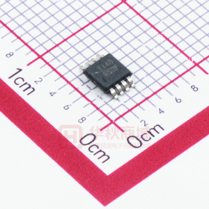
VS-505
Single Frequency VCSO
Features
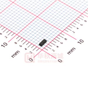
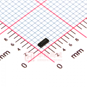
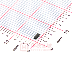
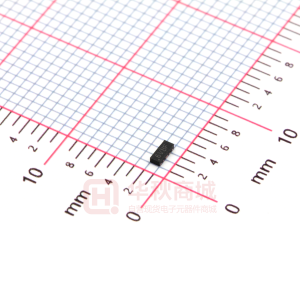
• Industry Standard Package, 9.1 x 13.8 x 3.7 mm • 5th Generation ASIC Technology for Ultra Low Jitter 120 fs-rms (fN = 622.08 MHz, 12 kHz to 20 MHz) 105 fs-rms (fN = 622.08 MHz, 50 kHz to 80 MHz) • Output Frequencies from 122.88 MHz to 1.00 GHz • Spurious Suppression, 90 dBc Typical • 2.5V or 3.3V Supply Voltage • LVPECL or LVDS Output Configurations • Tri-State Output Select (OD, OS, OE) • Compliant to EC RoHS Directive Pb
Applications
PLL circuits for Clock Smoothing and Frequency Translation Description • SONET / SDH • OTN (Optical Transport Network) • 10 GbE (Gigabit Ethernet) • 10 GFC (Gigabit Fibre Channel) • 40 GbE & 100 GbE • Synchronous Ethernet • WiMax
Vcc COutput Output
Standard GR-253-CORE ITU-T G.709/Y.1331 IEEE 802.3ae INCITS 364-2003 IEEE 802.3ba ITU-T G.8261 IEEE 802.16
Description
The VS-505 is a Voltage Controlled SAW Oscillator that operates at the fundamental frequency of the internal SAW filter. The SAW filter is a high-Q Quartz device that enables the circuit to achieve low phase jitter performance over a wide operating temperature range. A divider circuit is deployed for output frequencies less than 491.52 MHz. The oscillator is housed in a hermetically sealed leadless surface mount package and offered on tape and reel. It has a tri-state Output Select function that provides one of three conditions: Output Disable, Output Set, or Output Enable.
SAW
LVPECL LVDS 1 X
X=1,2,4
Vc
OSelect
Gnd
Vectron International, 267 Lowell Road, Hudson, NH 03051 Page 1 of 9
Tel: 1-88-VECTRON-1 • Web: www.vectron.com Rev: 01Apr2010
�VS-505 Single Frequency VCSO
Electrical Performance: 3.3V LV-PECL
Parameter Frequency
Nominal Frequency Absolute Pull Range Linearity Gain Transfer (Standard) Temperature Stability fN APR Lin KV fSTAB VCC ICC ICC 120 ±50 ±7 +445 ±100 2.97 3.3 73 60 VCC-1.3 750 1.5 180 180 50 90 150 190 280 130 472 200 -40 9.1 x 13.8 x 3.7 +85 3.63 75 VCC-1.1 1000 MHz ppm % ppm/V ppm V mA mA mV mV-pp V-pp mA ps-pp ps-pp % dBc fs-rms fs-rms fs-rms kΩ kΩ kHz °C mm 1,2,3 1,2,3,9 2,4,9 2,9 1,7 2,3 3 3 2,3 2,3 2,3 7 6,7 6,7 2,3 7 7,8 7,8 7,8 7 7 7 1,3
Symbol
Minimum
Typical
Maximum
Units
Notes
Supply
Voltage (± 10%) Current (Typical 50Ω Load) Current (No Load)
Outputs
Mid Level Single Ended Swing Differential Swing Current Rise Time Fall Time Symmetry Spurious Suppression Jitter (>491.52 MHz to 245.76 MHz to 122.88 MHz to 491.52 MHz, Jitter is Integrated across 50 kHz to 80 MHz. For Frequencies 100 mA.
Test Circuits & Output Load Configurations
+3.3V Vc (-3.00V to -0.30V) 0.10 μF OSelect 0.01 μF Vc OSelect Gnd Vcc COutput Output 0.01 μF 0.01 μF + + H (-0.55V to 0.00V) M (-1.90V to -1.40V) L (-3.30V to -2.75V) +2.0V 0.10 μF 0.01 μF Vcc COutput Output Or 0.01 μF 0.01 μF 10KΩ
1 2 3
6 5 4
Vc
1 2 3
6 5 4
OSelect Vee -1.3V
240Ω
240Ω
10KΩ
Functional Test: Allows use of standard power supply biasing configuration. Pull down resistors are used for LV-PECL outputs and are removed for with LVDS outputs. Since the LVDS outputs are AC coupled, the output DC levels cannot be measured.
V DMV Production Test: DC levels shown for Vee, OSelect, & Vc are for devices configured for 3.3V operation. Vee LV-PECL outputs are DC coupled to 50Ω test equipment. LVDS outputs are connected to a digital volt meter, then AC coupled to the test equipment. The digitial volt meter allows for Mid Level & Swing measurements.
+3.3V 0.10 μF 0.01 μF Vc OSelect Gnd Vcc COutput Output Z = 50Ω Z = 50Ω 100Ω Vc OSelect Gnd
+3.3V 0.10 μF 0.01 μF Vcc COutput Output Z = 50Ω Z = 50Ω 100Ω
1 2 3
6 5 4
1 2 3
6 5 4
240Ω
240Ω
LV-PECL to LV-PECL: For short transmission lengths, the pull down resistor values shown provide reasonable power consumption and waveform performance.
LVDS to LVDS: The 100Ω resistor should be removed if this load is provided internally within the LVDS receiver.
Vectron International, 267 Lowell Road, Hudson, NH 03051 Page 3 of 9
Tel: 1-88-VECTRON-1 • Web: www.vectron.com Rev: 01Apr2010
�VS-505 Single Frequency VCSO
Typical Characteristics: Vc Pull & Vc Pull Linearity
900 800 700 600 500 400 850.00 622.08 491.52 425.00 311.04 245.76 212.50 155.52 122.88 Kv = 459 ppm/V Kv = 443 ppm/V Kv = 458 ppm/V
Vc Pull
Frequency (ppm)
300 200 100 0 -100 -200 -300 -400 -500 -600 -700 0.00
TPull = 1240 ppm TPull = 1150 ppm TPull = 1258 ppm
0.30
0.60
0.90
1.20
1.50
1.80
2.10
2.40
2.70
3.00
3.30
Control Voltage (V)
10% 8% 6% 4%
Vc Linearity (%)
2% 0% -2% -4% -6% -8% -10% 0.30
850.00 622.08 491.52 425.00 311.04 245.76 212.50 155.52 122.88
Vc Pull Linearity
Max (0.3V to 3.0V) = 3.32% Min (0.3V to 3.0V) = -6.19%
0.60
0.90
1.20
1.50
1.80
2.10
2.40
2.70
3.00
Control Voltage (V)
Vectron International, 267 Lowell Road, Hudson, NH 03051 Page 4 of 9
Tel: 1-88-VECTRON-1 • Web: www.vectron.com Rev: 01Apr2010
�VS-505 Single Frequency VCSO
Typical Characteristics: Phase Noise & Jitter
-20 -30 -40 -50 -60 -70 Jitter (fs-rms) Frequency 12K-20M 850.00 104.7 622.08 116.3 491.25 128.8 425.00 142.9 311.04 169.2 245.76 185.1 212.50 205.0 155.52 235.3 122.88 275.1 Agilent E5052B 50K-40M 50K-80M 67.3 83.7 79.0 100.5 106.3 140.6 160.0 217.8 183.7 255.0 218.9 258.4 300.5 360.5 850.00 Fund 622.08 491.52 425.00 Div2 311.04 245.76 212.50 Div4 155.52 122.88 12K - 20M 50K - 80M
L(f) (dBc/Hz)
-80 -90 -100 -110 -120 -130 -140 -150 -160 10 100 1,000 10,000 100,000 1,000,000
10,000,000
100,000,000
Offset (Hz)
Vectron International, 267 Lowell Road, Hudson, NH 03051 Page 5 of 9
Tel: 1-88-VECTRON-1 • Web: www.vectron.com Rev: 01Apr2010
�VS-505 Single Frequency VCSO
Reliability
VI qualification includes aging at various extreme temperatures, shock and vibration, temperature cycling, and IR reflow simulation. The VS-505 family is capable of meeting the following qualification tests:
Environmental Compliance
Parameter Mechanical Shock Mechanical Vibration Solderability Gross and Fine Leak Resistance to Solvents Moisture Sensitivity Level Conditions MIL-STD-883, Method 2002 B MIL-STD-883, Method 2007 A MIL-STD-883, Method 2003 MIL-STD-883, Method 1014 MIL-STD-883, Method 2016 IPC/JEDEC J-STD-020, MSL1
Handling Precautions
Although ESD protection circuitry has been designed into the VS-505 proper precautions should be taken when handling and mounting. VI employs a human body model (HBM) and a charged-device model (CDM) for ESD susceptibility testing and design protection evaluation.
ESD Ratings
Model Human Body Model Charged Device Model Machine Model Minimum 2000 V 1000 V 200 V Conditions MIL-STD 883, Method 3015 JEDEC, JESD22-C101 JEDEC, JESD22-A115-A
Reflow Profile (IPC/JEDEC J-STD-020)
Parameter PreHeat Time Ramp Up Time Above 217 oC Time To Peak Temperature Time At 260 oC Ramp Down Symbol tS R UP tL t AMB-P tP R DN
260
Value 60 sec Min, 180 sec Max 3 oC/sec Max 60 sec Min, 150 sec Max 480 sec Max 20 sec Min, 40 sec Max 6 oC/sec Max tL R UP
Temperature (DegC)
217 200 150
The VS-505 is qualified to meet the JEDEC standard for Pb-Free assembly. The temperatures and time intervals listed are based on the Pb-Free small body requirements. The temperatures refer to the topside of the package, measured on the package body surface. The VS-505 should not be subjected to a wash process that will immerse it in solvents, NO CLEAN is the recommended procedure. The VS-505 is designed for pick and place reflow soldering. It should be reflowed once on topside position only. Terminal Plating: ENIG per IPC-4552 Electroless Ni = 3 - 6 µm Immersion Au = 0.05 µm Min
tP R DN
tS t AMB-P
25
Time (sec)
Vectron International, 267 Lowell Road, Hudson, NH 03051 Page 6 of 9
Tel: 1-88-VECTRON-1 • Web: www.vectron.com Rev: 01Apr2010
�VS-505 Single Frequency VCSO
Outline & Marking Diagram
13.80±0.15 [.543±.006] 6 5 4 7.62 [.300] 3.73±0.20 [.147±.008] 0.79 [.031] 0.76 [.030]
1.27 [.050]
Suggested Pad Layout
9.10±0.15 [.358±.006]
VS505 YWW CCC-CCCC XXXMXXX
1 2 3 12.70 [.500] 1.55 [.061]
2.95 [.116]
8.80 [.346]
0.51 [R0.020]
6.00±0.15 [.236±.006]
Y = Year WW = Week C = Option Codes XXXMXXX = Frequency (See Ordering Info)
3.00 [.118]
2.54 [.100] 5.08 [.200]
mm [inch]
1.02 [.040]
2.54 [.100]
mm [inch]
Pin Out
Pin Symbol Function
Control Voltage 1 VC 2 OSelect Output Select 3 GND Case and Electrical Ground 4 Output Output 5 COutput Complementary Output Power Supply Voltage 6 VCC Floating OSelect Always Results In OE
Output Select (Tri-State LV-CMOS)
Option
A
OS
Voltage Range
Result
OE OS OD OD OS OE
H (5VCC / 6) to VCC M (VCC / 2) ± 15%(VCC / 2) L Gnd to (VCC / 6) H (5VCC / 6) to VCC C M (VCC / 2) ± 15%(VCC / 2) L Gnd to (VCC / 6) OD = Outputs Disabled OS = Outputs Set (Output = H, COutput = L) OE = Outputs Enabled
Tape and Reel (EIA-481-2-A)
D Pin ID W2 F A C W1 N W Pull Off Direction Po ØDo
P1
B
Tape Dimensions (mm)
Dimension
Tolerance VS-505
Reel Dimensions (mm)
F Do
Typ 1.5
W
Typ 24
Po
Typ 4
P1
Typ 12
A
Typ 330
B
Min 1.5
C
Typ 13
D
Min 20.2
N
Min 100
W1
Typ 24.4
W2
Max 30.4
Typ 11.5
# Per Reel
200
Vectron International, 267 Lowell Road, Hudson, NH 03051 Page 7 of 9
Tel: 1-88-VECTRON-1 • Web: www.vectron.com Rev: 01Apr2010
�VS-505 Single Frequency VCSO
Standard Frequencies (MHz)
122.880000 167.331646 245.760000 491.520000 644.531250 718.863800 834.640000 125.000000 168.040678 307.200000 500.000000 657.421875 737.280000 877.968756 155.520000 173.370748 315.000000 531.250000 666.514286 739.200000 983.040000 156.250000 173.437500 320.000000 614.400000 669.326582 768.000000 1000.00000 160.000000 184.320000 368.640000 622.080000 672.000000 777.600000 161.132813 200.000000 400.000000 625.000000 715.538900 800.000000 166.628572 212.500000 425.000000 627.329620 716.800000 819.200000
Other Frequencies Available Upon Request.
Ordering Information
VS - 505 - E C E - K A A N – xxxMxxxxxx
Product Family
VS: VCSO
Frequency (See Above)
122M880000 – 1G00000000
Package
505: 9.1 x 13.8 x 3.7 mm
Other (Future Use)
N: N/A
Supply Voltage
E: 3.3V H: 2.5V
Oscillator Gain
A: Standard B: Low
Output Type
C: LVPECL D: LVDS
Control Logic (Tri-State)
A: L = OD, M = OS, H = OE C: L = OE, M = OS, H = OD
Operating Temperature
E: -40oC to 85oC
Absolute Pull Range
K: ± 50 ppm S: ± 100 ppm
Example: VS-505-ECE-KAAN-983M040000
Contact Information:
USA: Vectron International • 267 Lowell Rd. Hudson, NH 03051 Tel: 1-88-VECTRON-1 • Fax: 1-888-FAX-VECTRON EUROPE: Landstrasse, D-74924, Neckarbischofsheim, Germany Tel: 49 (0) 7268 8010 • Fax: 49 (0) 7268 801281 ASIA: 1F-2F, No 8 Workshop, No. 308 Fenju Road, WaiGaoQiao Free Trade Zone, Pudong, Shanghai, China 200131 Tel: 86 21 5048 0777 • Fax: 86 21 5048 1881 Vectron International reserves the right to make changes to the product(s) and or information contained herein without notice. No liability is assumed as a result of their use or application. No rights under any patent accompany the sale of any such product(s) or information.
Vectron International, 267 Lowell Road, Hudson, NH 03051 Page 8 of 9
Tel: 1-88-VECTRON-1 • Web: www.vectron.com Rev: 01Apr2010
�VS-505 Single Frequency VCSO
Revision History
Date
05Nov2008 24Feb2010 08Mar2010 01Apr2010
Approved
JM, BW BW JM JM
Description
Release Updated to reflect new global part numbering system. Marking drawing updated. Updated applications, frequency range, terminal plating, outline, frequency, and ordering options. Updated Vc filter model and outline.
Vectron International, 267 Lowell Road, Hudson, NH 03051 Page 9 of 9
Tel: 1-88-VECTRON-1 • Web: www.vectron.com Rev: 01Apr2010
�