VS-750
Dual Frequency VCSO
Features
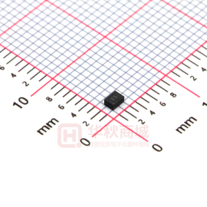
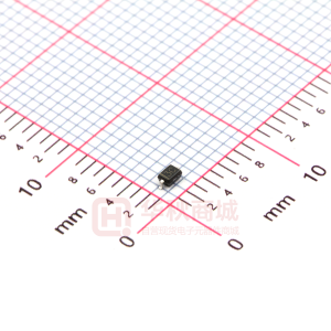
• 5 x 7.5 x 2.5 mm Package • Output Frequencies from 500 MHz to 850 MHz • 3.3 V Operation • Low Jitter < 0.25 ps-rms across 50 kHz to 80 MHz • LV-PECL Configuration with Fast Transition Times • Complementary Outputs • Frequency Select • Output Disable • Patent Pending Technology • Pb Product is free of lead and compliant to EC RoHS Directive
Applications
PLL circuits for Clock Smoothing and Frequency Translation Description • 1-2-4 Gigabit Fibre Channel • 10 Gigabit Fibre Channel • 10GbE LAN / WAN • OC-192
Vcc COutput Output
Standard INCITS 352-2002 INCITS 364-2003 IEEE 802.3ae ITU-T G.709 GR-253-CORE Issue3
• SONET / SDH
Description
SAW 1 SAW 2
Vc
OD
FS
Gnd
The VS-750 is a SAW based voltage controlled oscillator that operates at the fundamental frequencies of the internal SAW filters. These SAW filters are high-Q quartz devices that enable the circuit to achieve low phase jitter performance over a wide operating temperature range. The dual oscillator is housed in a hermetically sealed leadless surface mount package offered on tape and reel. It has a frequency select function that enables either “Frequency 1” or “Frequency 2.” It also has an output disable to facilitate on-board testing.
Vectron International, 267 Lowell Rd, Hudson NH 03051-4916
Tel: 1-88-VECTRON-1
Website: www.vectron.com Rev: 09Jan06
Page 1 of 7
�VS-750 Voltage Controlled SAW Oscillator
Electrical Performance
Parameter Frequency Nominal Frequency Absolute Pull Range Linearity Gain Transfer (See Pg 5) Temperature Stability Transition Time Supply Voltage Current (No Load) Outputs Mid Level Swing Current Rise Time Fall Time Symmetry Spurious Suppression Jitter (See Pg 5) Control Voltage Input Impedance Modulation Bandwidth Operating Temperature Package Size
1. 2. 3. 4. 5. 6. 7. 8.
Data Sheet
Symbol fN APR Lin KV fSTAB
Minimum
Typical 500 - 850
Maximum
Units MHz ppm % ppm/V ppm µsec
Notes 1,2,3 1,2,3,8 2,4,8 2,8 1,6 6 2,3 3 2,3 2,3 6 5,6 5,6 2,3 6 6,7 6 6 1,3
±50 ±5 +405 ±100 4 2.97 3.3 55 VCC-1.3 650 250 250 50 60 0.130 100 500 -40 5.0 x 7.5 x 2.5 85 3.63 70 VCC-1.2 950 20 400 400 55 0.250
VCC ICC
V mA V mV-pp mA ps ps % dBc ps-rms kΩ kHz °C mm
VCC-1.4 550 IOUT tR tF SYM φJ Zc BW TOP
45 50
See Standard Frequencies and Ordering Information (Pg 7). Parameters are tested with production test circuit below (Fig 1). Parameters are tested at ambient temperature with test limits guardbanded for specified operating temperature. Measured as the maximum deviation from the best straight-line fit, per MIL-0-55310. Measured from 20% to 80% of a full output swing (Fig 2). Not tested in production, guaranteed by design, verified at qualification. Integrated across 50 kHz to 80 MHz, per GR-253-CORE Issue3. Tested with Vc = 0.3V to 3.0V.
Vc (-1.0V to +1.7V) OE (-0.58V), OD (+0.59V) F1 (-0.58V), F2 (+0.59V)
1 2 3
12
Vcc (+2V)
10
COutput
80%
tR
tF
SYM = 100 x tA / tB
Vcc - 1.0V
Vee (-1.3V)
5
8 50Ω 50Ω
Output
Vcc - 1.3V
-1.3V: 5,13 Gnd: 4,6,7,9,11,14
20% Vcc - 1.6V
Test Circuit Notes: 1) To Permit 50Ω Measurement of Outputs, all DC Inputs are Biased Down 1.3V. 2) All Voltage Sources Contain Bypass Capacitors to Minimize Supply Noise. 3) 50Ω Terminations are Within Test Equipment.
tA tB
Figure 1. Test Circuit
Figure 2. 10K LV-PECL Waveform
Vectron International, 267 Lowell Rd, Hudson NH 03051-4916
Tel: 1-88-VECTRON-1
Website: www.vectron.com Rev: 09Jan06
Page 2 of 7
�VS-750 Voltage Controlled SAW Oscillator
Outline Diagram
12 11 10 9 8
Data Sheet
Pad Layout
13 14
VS750LG XX - XX VI YWW
1 2 4 3 7.50±0.15 [0.295±0.006] 5
7 6
5.10±0.15 [0.201±0.006]
1.02 [0.040] 1. 96 [0.077]
0.25 [0. 010]
1.27 [0.050] 0.64 [ 0.025] 4.14 [0.163]
1.30 [0.051] 1.02 [0.040] 2.49±0.18 [0.098±0.007]
1.52 [0.060]
1.27 [0.050] Y = Year WW = Week XX = Frequency Code (See Ordering Info) mm [inch]
1.02 [0.040] 0.20 [0.008] 1. 45 [0.057] 2.54 [0.100] 5.08 [0.200]
0.76 [0.030] 0.76 [0.030] R0.15 [R0.006]
0.10 [0.004]
2.07 1.27 [0.081] [0.050] 3.28 [ 0.129]
1.27 [0.050] 2.54 [0.100]
mm [inch]
Pin Out
Pin
1 2 3 4,6,7,9,11,14 5,13 8 10 12
Marking Key
Symbol
VC OD FS NC Gnd Output COutput VCC
Function
VCSO Control Voltage Output Disable (See Control Logic) Frequency Select (F1 or F2) No Connection (Suggest to Gnd) Case and Electrical Ground VCSO Output VCSO Complementary Output Power Supply Voltage (3.3 V ±10%)
Position 6
L = LFF
Position 7
G = GNN H = HNN
Control Logic (LV-CMOS)
OD
0 0 1
FS
0 1 0
Operation
F1 F2 Disabled
Tape and Reel (EIA-481-2-A)
Po
ØDo W2
F W D C N A
P1
W1
B
Tape Dimensions (mm)
Dimension
Tolerance VS-750
Reel Dimensions (mm)
F Do
Typ 1.5
W
Typ 16
Po
Typ 4
P1
Typ 8
A
Typ 178
B
Min 1.5
C
Typ 13
D
Min 20.2
N
Min 50
W1
Typ 16.4
W2
Max 22.4
Typ 7.5
# Per Reel
200
Vectron International, 267 Lowell Rd, Hudson NH 03051-4916
Tel: 1-88-VECTRON-1
Website: www.vectron.com Rev: 09Jan06
Page 3 of 7
�VS-750 Voltage Controlled SAW Oscillator
Absolute Maximum Ratings
Parameter Power Supply Input Current Output Current Voltage Control Range Storage Temperature Soldering Temperature / Duration Symbol VCC IIN IOUT VC TSTR TPEAK / t P Ratings 0 to 6 100 25 0 to VCC -55 to 125 260 / 40
Data Sheet
Unit V mA mA V °C °C / sec
Stresses in excess of these absolute maximum ratings can permanently damage the device. Also, exposure to these absolute maximum ratings for extended periods can adversely affect device reliability. Functional operation is not implied at these or any other conditions in excess of those represented in the operational sections of this datasheet. Permanent damage is also possible if any device input (Vc, FS, or OD) draws greater than 100 mA.
Suggested Output Load Configurations
0.10 µF 0.0 1 µF +3 .3 V 0.10 µF 0.01 µF +3 .3 V +3 .3 V
15 0Ω
15 0Ω
Vc OD FS Gn d
1 2 3 5
12 10 8
Vcc COutp ut Outp ut Z = 50 Ω Z = 50 Ω 100Ω
Vc OD FS Gn d
1 2 3 5
12 10 8
Vcc COutp ut Outp ut Z = 50Ω Z = 50Ω
40Ω
40 Ω
49Ω
49 Ω
Gn d: 5,13 NC o r Gn d: 4,6,7,9,11,14
240 Ω
24 0Ω
Gn d: 5,13 NC o r Gn d: 4,6,7,9,11,1 4 LV- PE CL to LVDS : Re stricted for sh ort tran smission len gths. Co nfig urati on ma y requir e modification de pe nd ing o n LV DS re ceiver.
LV- PE CL to LV -P ECL: Fo r sh or t transmission length s, the p owe r co nsum ption co ul d be r ed uced by remo ving th e 10 0Ω re sisto r an d d oubling the va lue of th e pu ll do wn re sistors. +3 .3 V
0.10 µF 0.0 1 µF
0.10 µF 0.01 µF
+2 .0 V
Vc OD FS Gn d
1 2 3 5
12 10 8
Vcc COutp ut Outp ut 0.01 µF 0.01 µF
Vc OD FS -1 .3 V 24 0Ω
1 2 3 5
12 10 8
Vcc COutp ut Outp ut
Gn d: 5,13 NC o r Gn d: 4,6,7 ,9 ,11,1 4
240 Ω
-1.3V : 5 ,13 NC o r Gn d: 4,6,7,9,11,1 4 P roduc tion Te st : A llo ws d ire ct DC cou pli ng in to 50 Ω me asu rem ent e quipment. Mu st b ias the p owe r supplys as shown. S imil ar to Figu re 1 .
Funct iona l Te st: A llows stan da rd po wer su pp ly co nfig ura ti on . S ince A C cou ple d, th e LV -P ECL leve ls ca nn ot b e me asur ed .
Vectron International, 267 Lowell Rd, Hudson NH 03051-4916
Tel: 1-88-VECTRON-1
Website: www.vectron.com Rev: 09Jan06
Page 4 of 7
�VS-750 Voltage Controlled SAW Oscillator
Typical Characteristics
800
Data Sheet
At Ambient (22.5°C)
600 400
Typical Gain Transfer @ 622.0800 = +415 ppm/V Typical Gain Transfer @ 644.5313 = +399 ppm/V
Frequency (PPM)
200 0 -200 -400 -600 -800 0.3 0.6 0.9 1.2 1.5 1.8 2.1 2.4 2.7 3
622 Vc Pull 644 Vc Pull y = 415.29x - 605.56 y = 398.69x - 578.48 Linear (622 Vc Pull) Linear (644 Vc Pull)
Control Voltage (V)
-95
Typical Calculated Jitter @ Vc = 1.65V
-100 -105 -110 1/f -115
OC-192 Spec F1 = 622 F2 = 644
SONET OC-48 (12kHz-20MHz) = 0.23 ps-rms; 1.61 ps-pp SONET OC-192 (50kHz-80MHz) = 0.13 ps-rms; 0.91 ps-pp
3
L(f) (dBc/Hz)
-120 1/f -125 -130 -135 -140 -145 -150 -155 10 100
2
1/f1
OC-192 Spec Equivalent to 0.25 ps-rms @ 500 MHz
1,000
10,000
100,000
Offset (kHz)
Vectron International, 267 Lowell Rd, Hudson NH 03051-4916 Tel: 1-88-VECTRON-1 Website: www.vectron.com Rev: 09Jan06
Page 5 of 7
�VS-750 Voltage Controlled SAW Oscillator
Reliability
Data Sheet
VI qualification includes aging at various extreme temperatures, shock and vibration, temperature cycling, and IR reflow simulation. The VS-750 family is capable of meeting the following qualification tests:
Environmental Compliance
Parameter Mechanical Shock Mechanical Vibration Solderability Gross and Fine Leak Resistance to Solvents Conditions MIL-STD-883, Method 2002 MIL-STD-883, Method 2007 MIL-STD-883, Method 2003 MIL-STD-883, Method 1014 MIL-STD-883, Method 2016
Handling Precautions
Although ESD protection circuitry has been designed into the VS-750 proper precautions should be taken when handling and mounting. VI employs a human body model (HBM) and a man man model (MM) for ESD susceptibility testing and design protection evaluation.
ESD Ratings
Model Human Body Model Man Man Model Minimum 1500 V 200 V Conditions MIL-STD 883, Method 3015 V/JESD22-A115-A
Reflow Profile (IPC/JEDEC J-STD-020C)
Parameter PreHeat Time Ramp Up Time Above 217 oC Time To Peak Temperature Time At 260 oC Ramp Down Symbol tS R UP tL t AMB-P tP R DN
260
Value 60 sec Min, 180 sec Max 3 oC/sec Max 60 sec Min, 150 sec Max 480 sec Max 20 sec Min, 40 sec Max 6 oC/sec Max tL R UP tP R DN
Temperature (DegC)
The device has been qualified to meet the JEDEC standard for Pb-Free assembly. The temperatures and time intervals listed are based on the Pb-Free small body requirements. The temperatures refer to the topside of the package, measured on the package body surface. The VS-750 device is hermetically sealed so an aqueous wash is not an issue. Terminal Plating: Electroless Gold Plate over Nickel Plate
217 200
150
tS t AMB-P
25
Time (sec)
Vectron International, 267 Lowell Rd, Hudson NH 03051-4916 Tel: 1-88-VECTRON-1 Website: www.vectron.com Rev: 09Jan06
Page 6 of 7
�VS-750 Voltage Controlled SAW Oscillator
Standard Frequencies (MHz)
531.2500 P8 629.9878 PA 669.6429 R1 707.3527 TC 569.1964 P9 644.5313 P4 672.1627 R5 777.6000 T4 622.0800 P2 647.2508 PK 690.5692 R4 805.6641 TA 624.6938 PD 657.4219 PB 693.4830 R6 625.0000 P3 666.5143 P5 693.7500 R8
Data Sheet
627.3296 P7 669.3266 R3 704.3806 TG
1. Other frequencies available upon request, please contact VI for details. 2. Frequency 1 must be lower than Frequency 2. Not all combinations are available.
Ordering Information
VS - 750 - L F F - H N N - P2 - P4
Product Family
VS: VCSO
Frequency 2
See Above
Package
750: 5 x 7.5 x 2.5 mm
Frequency 1
See Above
Input
L: 3.3 V
Other (Future Use)
N: N/A
Output
F: LV-PECL
Other (Future Use)
N: N/A
Operating Temperature
F: -40 to 85 °C
Absolute Pull Range
G: +/- 50 ppm H: +/- 100 ppm
For Additional Information, Please Contact:
USA: Vectron International, 267 Lowell Rd, Hudson, NH 03051 . . . . Tel: 1-88-VECTRON-1 EUROPE: . . . . . . . . . . . . . . . . . . . . . . . . . . . . . . . . . . . . . . . . . . . . . . Tel: +49 (0) 3328-4784-17 ASIA: . . . . . . . . . . . . . . . . . . . . . . . . . . . . . . . . . . . . . . . . . . . . . . . . . . Tel: +86-21-28909740 Fax: 1-888-FAX-VECTRON Fax: +49 (0) 3328-4784-30 Fax: +86-21-28909240
Vectron International reserves the right to make changes to the product(s) and or information contained herein without notice. No liability is assumed as a result of their use or application. No rights under any patent accompany the sale of any such product(s) or information.
Vectron International, 267 Lowell Rd, Hudson NH 03051-4916
Tel: 1-88-VECTRON-1
Website: www.vectron.com Rev: 09Jan06
Page 7 of 7
�