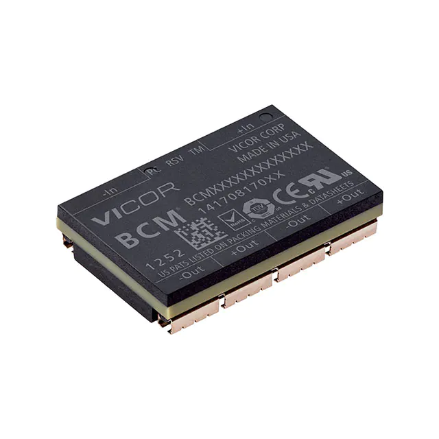
BCM48B x 120 y 300A00
PRELIMINARY DATASHEET
BCM™ Bus Converter
FEATURES
S
®
C
US
C
NRTL
US
• 48 Vdc – 12 Vdc 300 W Bus Converter • High efficiency (>96%) reduces system
power consumption
• High power density (>1022 W/in3)
reduces power system footprint by >40%
• Contains built-in protection features:
Undervoltage Overvoltage Lockout Overcurrent Protection Short circuit Protection Overtemperature Protection
• Provides enable/disable control,
internal temperature monitoring
• Can be paralleled to create multi-kW arrays
TYPICAL APPLICATIONS
DESCRIPTION The V•I Chip™ bus converter is a high efficiency (>96%) Sine Amplitude Converter™ (SAC™) operating from a 38 to 55 Vdc primary bus to deliver an isolated, unregulated 9.5 to 13.8 output. The Sine Amplitude Converter offers a low AC impedance beyond the bandwidth of most downstream regulators; therefore capacitance normally at the load can be located at the input to the Sine Amplitude Converter. Since the transformation ratio of the BCM48BF120T300A00 is 1/4, the capacitance value can be reduced by a factor of 16x, resulting in savings of board area, materials and total system cost. The BCM48BF120T300A00 is provided in a V•I Chip package compatible with standard pick-and-place and surface mount assembly processes. The co-molded V•I Chip package provides enhanced thermal management due to a large thermal interface area and superior thermal conductivity. The high conversion efficiency of the BCM48BF120T300A00 increases overall system efficiency and lowers operating costs compared to conventional approaches. PART NUMBERING
PART NUMBER PACKAGE STYLE PRODUCT GRADE
• High End Computing Systems • Automated Test Equipment • High Density Power Supplies • Communications Systems
BCM48B x 120 y 300A00
F = J-Lead T = Through hole
T = -40° to 125°C M = -55° to 125°C
For Storage and Operating Temperatures see Section 6.0 General Characteristics
TYPICAL APPLICATION
enable / disable switch SW1 F1
PC TM
BCM Bus Converter
+In +Out
TM
VIN -In -Out
L O A D
V•I CHIP CORP. (A VICOR COMPANY) 25 FRONTAGE RD. ANDOVER, MA 01810 800-735-6200
v i c o r p o w e r. c o m
Rev. 1.2 7/2011
Page 1 of 18
�PRELIMINARY DATASHEET
1.0 ABSOLUTE MAXIMUM VOLTAGE RATINGS
BCM48B x 120 y 300A00
The absolute maximum ratings below are stress ratings only. Operation at or beyond these maximum ratings can cause permanent damage to the device. MIN MAX UNIT MAX UNIT MIN +IN to –IN . . . . . . . . . . . . . . . . . . . . . . . VIN slew rate (operational) . . . . . . . . . Isolation voltage, input to output . . . . +OUT to –OUT . . . . . . . . . . . . . . . . . . . Output current transient (< = 10 ms, < = 10% DC) . . . . . . . . . . . . -1 -3 -1 -1 60 1 2250 16 37.5 V V/µs V V A Output current average . . . . . . . . . . . . PC to –IN . . . . . . . . . . . . . . . . . . . . . . . . TM to –IN . . . . . . . . . . . . . . . . . . . . . . . Operating IC junction temperature . . Storage temperature . . . . . . . . . . . . . . -2 -0.3 -0.3 -40 -40 30 20 7 125 125 A V V °C °C
2.0 ELECTRICAL CHARACTERISTICS
Specifications apply over all line and load conditions unless otherwise noted; Boldface specifications apply over the temperature range of -40°C < TC < 100°C (T-Grade); All other specifications are at TC = 25ºC unless otherwise noted.
ATTRIBUTE POWERTRAIN Input voltage range, continuous Input voltage range, transient Quiescent current VIN to VOUT time VIN_DC VIN_TRANS IQ TON1 Full current or power supported, 50 ms max, 10% duty cycle max Disabled, PC Low VIN = 48 V, PC floating VIN = 48 V, TC = 25ºC No load power dissipation PNL VIN = 48 V VIN = 38 V to 55 V, TC = 25ºC VIN = 38 V to 55 V Inrush current peak DC input current Transformation ratio Output power (average) Output power (peak) Output current (average) Output current (peak) IINR_P IIN_DC K POUT_AVG POUT_PK IOUT_AVG IOUT_PK 10 ms max, IOUT_AVG ≤ 30 A VIN = 48 V, IOUT = 25 A; Tc = 25°C Efficiency (ambient) 95.0 93.5 94.5 94.5 80 4.9 6.3 8.8 1.85 COUT = 0 F, IOUT = 25 A, VIN = 48 V, 20 MHz BW, Section 10 Frequency up to 30 MHz, Simulated J-lead model Effective value at 12 VOUT 0 6.7 9.0 11.5 1.95 150 600 47 1000 9.0 13.4 14.0 2.05 285 95.5 95.6 % % mΩ mΩ mΩ MHz mV pH µF µF 96.0 % VIN = 38 V to 55 V, IOUT = 25 A; Tc = 25°C VIN = 48 V, IOUT = 13 A; Tc = 25°C Efficiency (hot) Efficiency (over load range) VIN = 48 V, IOUT = 25 A; Tc = 100°C 5 A < IOUT < 25 A IOUT = 25 A, Tc = -40°C IOUT = 25 A, Tc = 25°C IOUT = 25 A, TC = 100°C 10 ms max, POUT_AVG ≤ 300 W Worse case of: VIN = 55 V, COUT = 1000 µF, RLOAD = 391 mΩ At POUT = 300 W K = VOUT / VIN, at no load 1/4 300 350 30 37.5 3 340 38 38 0.5 450 5.3 55 55 1.0 620 6.5 15 9 17 W V V mA ms SYMBOL CONDITIONS / NOTES MIN TYP MAX UNIT
10
20
8.8
A
A V/V W W A A
ηAMB ηHOT η20%
ROUT_COLD ROUT_AMB ROUT_HOT FSW VOUT_PP LOUT_PAR COUT_INT COUT_EXT
Output resistance
Switching frequency Output voltage ripple Output inductance (parasitic) Output capacitance (internal) Output capacitance (external)
V•I CHIP CORP. (A VICOR COMPANY) 25 FRONTAGE RD. ANDOVER, MA 01810 800-735-6200
v i c o r p o w e r. c o m
Rev. 1.2 7/2011
Page 2 of 18
�PRELIMINARY DATASHEET
BCM48B x 120 y 300A00
2.0 ELECTRICAL CHARACTERISTICS (CONT.)
ATTRIBUTE SYMBOL CONDITIONS / NOTES MIN TYP MAX UNIT
PROTECTION Input overvoltage lockout threshold Input overvoltage recovery threshold Input overvoltage lockout hysteresis Overvoltage lockout response time Fault recovery time Input undervoltage lockout threshold Input undervoltage recovery threshold Input undervoltage lockout hysteresis Undervoltage lockout response time Output overcurrent trip threshold Output overcurrent response time constant Short circuit protection trip threshold Short circuit protection response time Thermal shutdown threshold VIN_OVLO+ VIN_OVLOVIN_OVLO_HYST TOVLO TAUTO_RESTART VIN_UVLOVIN_UVLO+ VIN_UVLO_HYST TUVLO IOCP TOCP ISCP TSCP TJ_OTP 125 Effective internal RC filter 30 1 30 240 28.5 28.5 55.1 55.1 58.5 58.0 1.2 8 300 31.1 33.7 1.6 8 39 5.3 55 380 37.4 37.4 60.0 60.0 V V V µs ms V V V µs A ms A µs ºC
Safe Operating Area Average & Peak
375 50.00
350
43.75
325
37.50
300
31.25
275
25.00
250
18.75
225
12.50
200 8.70 9.23 9.76 10.29 10.82 11.36 11.89 12.42 12.95 13.48
6.25 14.01
Output Voltage (V)
P (ave) P (pk), < 10 ms I (ave) I (pk), < 10 ms
Figure 1 — Safe operating area
V•I CHIP CORP. (A VICOR COMPANY) 25 FRONTAGE RD. ANDOVER, MA 01810 800-735-6200
v i c o r p o w e r. c o m
Rev. 1.2 7/2011
Page 3 of 18
Output Current (A)
Output Power (W)
�PRELIMINARY DATASHEET
BCM48B x 120 y 300A00
3.0 SIGNAL CHARACTERISTICS
Specifications apply over all line and load conditions unless otherwise noted; Boldface specifications apply over the temperature range of -40°C < TC < 100°C (T-Grade); All other specifications are at TC = 25°C unless otherwise noted.
PRIMARY CONTROL : PC • The PC pin enables and disables the BCM. When held low, • PC pin outputs 5 V during normal operation. PC pin internal bias the BCM is disabled. level drops to 2.5 V during fault mode, provided VIN remains in the valid range. • In an array of BCM modules, PC pins should be interconnected to synchronize start up and permit start up into full load conditions. SIGNAL TYPE STATE Regular Operation ANALOG OUTPUT Standby Transition Start Up Start Up Regular Operation DIGITAL INPUT / OUPUT Standby ATTRIBUTE PC voltage PC available current PC source (current) PC resistance (internal) PC capacitance (internal) PC load resistance PC time to start PC enable threshold PC disable duration PC threshold hysteresis Transition PC enable to VOUT time PC disable to standby time PC fault response time SYMBOL VPC IPC_OP IPC_EN RPC_INT CPC_INT RPC_S TON1 VPC_EN TPC_DIS_T Minimum time before attempting re-enable VPC_HYSTER TON2 TPC-DIS TFR_PC From fault to PC = 2 V VIN = 48 V for at least TON1 ms Internal pull down resistor Section 7 To permit regular operation 60 340 2.0 1 50 50 100 4 100 150 10 450 2.5 620 3.0 CONDITIONS / NOTES MIN 4.7 2.0 50 50 TYP 5.0 3.5 100 150 400 1000 MAX UNIT 5.3 5.0 V mA µA kΩ pF kΩ ms V s mV µs µs µs
TEMPERATURE MONITOR : TM • The TM pin monitors the internal temperature of the controller IC • Can be used as a "Power Good" flag to verify that within an accuracy of ±5°C. the BCM module is operating. • Is used to drive the internal comparator for Overtemperature Shutdown. SIGNAL TYPE STATE ATTRIBUTE TM voltage range TM voltage reference ANALOG OUTPUT Regular Operation TM available current TM gain TM voltage ripple DIGITAL OUTPUT (FAULT FLAG) Transition TM capacitance (external) TM fault response time Standby TM voltage TM pull down (internal) SYMBOL VTM VTM_AMB ITM ATM VTM_PP CTM_EXT TFR_TM VTM_DIS RTM_INT Internal pull down resistor 25 From fault to TM = 1.5 V 10 0 40 50 CTM = 0 pF, VIN = 48 V, IOUT = 25 A TJ controller = 27°C CONDITIONS / NOTES MIN 2.12 2.95 100 10 120 200 50 3.00 TYP MAX UNIT 4.04 3.05 V V µA mV/°C mV pF µs V kΩ
RESERVED : RSV Reserved for factory use. No connection should be made to this pin.
V•I CHIP CORP. (A VICOR COMPANY) 25 FRONTAGE RD. ANDOVER, MA 01810 800-735-6200
v i c o r p o w e r. c o m
Rev. 1.2 7/2011
Page 4 of 18
�VOVLO+ VOVLO–
1
2
3 5
4 6
4.0 TIMING DIAGRAM
PRELIMINARY DATASHEET
v i c o r p o w e r. c o m
C B
VIN
NL
VUVLO+ VUVLO–
PC
5V 3V
3V
5V 2.5 V
C 500mS before retrial
Vout
G D A E F
LL • K
IOUT ISSP IOCP
H
TM
3 V @ 27°C
V•I CHIP CORP. (A VICOR COMPANY) 25 FRONTAGE RD. ANDOVER, MA 01810 800-735-6200
0.4 V
Notes:
A: TON1 B: TOVLO* C: TAUTO_RESTART D:TUVLO E: TON2 F: TOCP G: TPC–DIS H: TSCP**
1: Controller start 2: Controller turn off 3: PC release
4: PC pulled low 5: PC released on output SC 6: SC removed
– Timing and signal amplitudes are not to scale – Error pulse width is load dependent
*Min value switching off **From detection of error to power train shutdown
BCM48B x 120 y 300A00
Page 5 of 18
Rev. 1.2 7/2011
�PRELIMINARY DATASHEET
5.0 APPLICATION CHARACTERISTICS
BCM48B x 120 y 300A00
The following values, typical of an application environment, are collected at TC = 25ºC unless otherwise noted. See associated figures for general trend data.
No Load Power Dissipation vs. Line
No Load Power Dissipation (W)
12
Full Load Efficiency vs. TCASE
96.5
Full Load Efficiency (%)
40 42 44 46 25°C 47 49 51 53 55
11 10 9 8 7 6 5 4 38
96.0 95.5 95.0 94.5 94.0 -40 -20 0 20 40 60 80 100
Input Voltage (V)
-40°C 100°C
Case Temperature (°C)
VIN : 38 V 48 V 55 V
Figure 2 — No load power dissipation vs. VIN
Figure 3 — Full load efficiency vs. temperature; VIN
Efficiency & Power Dissipation -40°C Case
97 92 30 25 20 98
Efficiency & Power Dissipation 25°C Case
24
Power Dissipation (W)
η
PD
Efficiency (%)
87 82 77 72 67 0 5 38 V 48 V 10 55 V 15 38 V 20 48 V
15 10 5 0 25
Efficiency (%)
93
18
88
PD
12
83
6
78 0 5 10 15 20
0 25
Load Current (A)
VIN: 55 V VIN: 38 V 48 V
Load Current (A)
55 V 38 V 48 V 55 V
Figure 4 — Efficiency and power dissipation at TC = -40°C
Figure 5 — Efficiency and power dissipation at TC = 25°C
Efficiency & Power Dissipation 100°C Case
98 24 14
ROUT vs. TCASE at VIN = 48 V
Power Dissipation (W)
12
Efficiency (%)
93
η
PD
18
Rout (mΩ)
10 8 6 4 -40 -20 0 20 40 60 80 100
88
12
83
6
78 0 VIN: 38 V 5 48 V 10 55 V 15 38 V 20 48 V
0 25 55 V
Load Current (A)
Case Temperature (°C)
I OUT : 12.5 A 25 A
Figure 6 — Efficiency and power dissipation at TC = 100°C
Figure 7 — ROUT vs. temperature
V•I CHIP CORP. (A VICOR COMPANY) 25 FRONTAGE RD. ANDOVER, MA 01810 800-735-6200
v i c o r p o w e r. c o m
Rev. 1.2 7/2011
Page 6 of 18
Power Dissipation (W)
η
�PRELIMINARY DATASHEET
BCM48B x 120 y 300A00
Output Voltage Ripple vs. Load
145 125
Ripple (mV pk-pk)
105 85 65 45 25 0 5 VIN : 10 48 V 15 20 25
Load Current (A)
Figure 8 — VRIPPLE vs. IOUT ; No external COUT. Board mounted module, scope setting : 20 MHz analog BW
Figure 9 — Full load ripple, 330 µF CIN; No external COUT. Board mounted module, scope setting : 20 MHz analog BW
Figure 10 — Start up from application of PC; VIN pre-applied COUT = 1000 µF
Figure 11 — 0 A– 25 A transient response: CIN = 330 µF, IIN measured prior to CIN , no external COUT
Figure 12 — 25 A – 0 A transient response: CIN = 330 µF, IIN measured prior to CIN , no external COUT
Rev. 1.2 7/2011
Page 7 of 18
v i c o r p o w e r. c o m
V•I CHIP CORP. (A VICOR COMPANY) 25 FRONTAGE RD. ANDOVER, MA 01810 800-735-6200
�PRELIMINARY DATASHEET
6.0 GENERAL CHARACTERISTICS
BCM48B x 120 y 300A00
Specifications apply over all line and load conditions unless otherwise noted; Boldface specifications apply over the temperature range of -40ºC < TJ < 100ºC (T-Grade); All other specifications are at TJ = 25°C unless otherwise noted.
ATTRIBUTE MECHANICAL Length Width Height Volume Weight L W H Vol W Nickel Lead finish Palladium Gold THERMAL Operating temperature Thermal resistance Thermal capacity ASSEMBLY Peak compressive force applied to case (Z-axis) Storage temperature Moisture sensitivity level TST MSL ESDHBM ESD withstand ESDCDM SOLDERING Peak temperature during reflow Peak time above 217°C Peak heating rate during reflow Peak cooling rate post reflow SAFETY Working voltage (IN – OUT) Isolation voltage (hipot) Isolation capacitance Isolation resistance VIN_OUT VHIPOT CIN_OUT RIN_OUT Unpowered unit At 500 Vdc MIL-HDBK-217Plus Parts Count 25°C Ground Benign, Stationary, Indoors / Computer Profile Telcordia Issue 2 - Method I Case III; 25°C Ground Benign, Controlled cTUVus cURus CE Mark RoHS 6 of 6 2,250 2500 10 6.03 7.94 3200 3800 60 VDC VDC pF MΩ MHrs MHrs MSL 4 245 °C °C 60 1.5 1.5 90 3 6 s °C/s °C/s Supported by J-lead only BCM48BF120T300A00 (T-Grade) BCM48BF120M300A00 (M-Grade) MSL 4 Human Body Model, "JEDEC JESD 22-A114D.01"Class 1D Charge Device Model, "JEDEC JESD 22-C101-D" -40 -65 6 5.41 125 125 lbs lbs / in2 °C °C TJ BCM48BF120T300A00 (T-Grade) BCM48BF120M300A00 (M-Grade) Isothermal heatsink and isothermal internal PCB -40 -55 1 5 125 125 °C °C °C/W Ws/°C 0.51 0.02 0.003 No heat sink 32.25 / [1.270] 21.75 / [0.856] 6.48 / [0.255] 32.50 / [1.280] 22.00 / [0.866] 6.73 / [0.265] 4.81 / [0.294] 14.5 / [0.512] 2.03 0.15 0.051 µm 32.75 / [1.289] 22.25 / [0.876] 6.98 / [0.275] mm/[in] mm/[in] mm/[in] cm3/[in3] g/[oz] SYMBOL CONDITIONS / NOTES MIN TYP MAX UNIT
φJC
1000 V 400
MTBF
Agency approvals / standards
V•I CHIP CORP. (A VICOR COMPANY) 25 FRONTAGE RD. ANDOVER, MA 01810 800-735-6200
v i c o r p o w e r. c o m
Rev. 1.2 7/2011
Page 8 of 18
�PRELIMINARY DATASHEET
7.0 USING THE CONTROL SIGNALS PC, TM Primary Control (PC) pin can be used to accomplish the following functions: • Logic enable and disable for module: Once Ton1 time has been satisfied, a PC voltage greater than Vpc_en will cause the module to start. Bringing PC lower than Vpc_dis will cause the module to enter standby. • Auxiliary voltage source: Once enabled in regular operational conditions (no fault), each BCM module PC provides a regulated 5 V, 3.5 mA voltage source. • Synchronized start up: In an array of parallel modules, PC pins should be connected to synchronize start up across units. This permits the maximum load and capacitance to scale by the number of paralleled modules. • Output disable: PC pin can be actively pulled down in order to disable the module. Pull down impedance shall be lower than 60 Ω. • Fault detection flag: The PC 5 V voltage source is internally turned off as soon as a fault is detected. • Note that PC can not sink significant current during a fault condition. The PC pin of a faulted module will not cause interconnected PC pins of other modules to be disabled. Temperature Monitor (TM) pin provides a voltage proportional to the absolute temperature of the converter control IC. It can be used to accomplish the following functions: • Monitor the control IC temperature: The temperature in Kelvin is equal to the voltage on the TM pin scaled by 100. (i.e. 3.0 V = 300 K = 27ºC). If a heat sink is applied, TM can be used to protect the system thermally. • Fault detection flag: The TM voltage source is internally turned off as soon as a fault is detected. For system monitoring purposes microcontroller interface faults are detected on falling edges of TM signal.
BCM48B x 120 y 300A00
V•I CHIP CORP. (A VICOR COMPANY) 25 FRONTAGE RD. ANDOVER, MA 01810 800-735-6200
v i c o r p o w e r. c o m
Rev. 1.2 7/2011
Page 9 of 18
�+Vin
Vcc V2
PRELIMINARY DATASHEET
8.0 BCM48BF120T300A00 BLOCK DIAGRAM
v i c o r p o w e r. c o m
“Wake-Up” Power And Logic
+Vout
Q3
Power Transformer
Q5
18.5 V
Q1
Primary Stage & Resonant Tank Gate Drive supply Primary Gate Drive
Lr Q2 Cr Q6 One shot delay Ton1
COUT
-Vin
Q4
-Vout
Synchronous Rectification
Adaptive Soft Start
Secondary Gate Drive
Modulator
Enable
Vcc Vin
PC Pull-Up & Source
Primary current sensing
100 uA
UVLO OVLO
5 V, 2 mA min Vref
Start up & Fault logic
Fast current Limit
Overcurrent Protection
3.1 V
∫
Slow current limit
PC
150 K
V•I CHIP CORP. (A VICOR COMPANY) 25 FRONTAGE RD. ANDOVER, MA 01810 800-735-6200
2.5 V
1K
1000 pF
TM
40 K
Temperature dependent voltage source Overtemperature Protection
Temp_Vref
0.01 F
BCM48B x 120 y 300A00
Page 10 of 18
Rev. 1.2 7/2011
�PRELIMINARY DATASHEET
9.0 SINE AMPLITUDE CONVERTER™ POINT OF LOAD CONVERSION
973 pH LLIN = 5 nH IN = 5.7 nH IOUT IOUT
BCM48B x 120 y 300A00
ROUT ROUT 9.0 mΩ
LOUT = 600 pH
+
RCIN RCIN 0.57 mΩ
V VIN IN CIN CIN 2 µF 109 mA
Q IIQ
V•I
1/4 • IOUT
3.13 Ω
R RCOUT COUT 47 µF
+
430 µΩ
+ – K
+ –
1/4 • VIN
COUT COUT
VOUT VOUT
–
–
Figure 13 — V•I ChipTM module AC model
The Sine Amplitude Converter (SAC™) uses a high frequency resonant tank to move energy from input to output. (The resonant tank is formed by Cr and leakage inductance Lr in the power transformer windings as shown in the BCM™ module Block Diagram. See Section 8). The resonant LC tank, operated at high frequency, is amplitude modulated as a function of input voltage and output current. A small amount of capacitance embedded in the input and output stages of the module is sufficient for full functionality and is key to achieving power density. The BCM48BF120T300A00 SAC can be simplified into the preceeding model. At no load: VOUT = VIN • K K represents the “turns ratio” of the SAC. Rearranging Eq (1): V K = OUT VIN In the presence of load, VOUT is represented by: VOUT = VIN • K – IOUT • ROUT and IOUT is represented by: IOUT = IIN – IQ K (4) (3) (2) (1)
ROUT represents the impedance of the SAC, and is a function of the RDSON of the input and output MOSFETs and the winding resistance of the power transformer. IQ represents the quiescent current of the SAC control, gate drive circuitry, and core losses. The use of DC voltage transformation provides additional interesting attributes. Assuming that ROUT = 0 Ω and IQ = 0 A, Eq. (3) now becomes Eq. (1) and is essentially load independent, resistor R is now placed in series with VIN.
R VIN Vin
+ –
SAC™ SAC K = 1/4 K = 1/32
Vout VOUT
Figure 14 — K = 1/4 Sine Amplitude Converter™ with series input resistor
The relationship between VIN and VOUT becomes: VOUT = (VIN – IIN • R) • K Substituting the simplified version of Eq. (4) (IQ is assumed = 0 A) into Eq. (5) yields: VOUT = VIN • K – IOUT • R • K2 (6) (5)
V•I CHIP CORP. (A VICOR COMPANY) 25 FRONTAGE RD. ANDOVER, MA 01810 800-735-6200
v i c o r p o w e r. c o m
Rev. 1.2 7/2011
Page 11 of 18
�PRELIMINARY DATASHEET
This is similar in form to Eq. (3), where ROUT is used to represent the characteristic impedance of the SAC™. However, in this case a real R on the input side of the SAC is effectively scaled by K2 with respect to the output. Assuming that R = 1 Ω, the effective R as seen from the secondary side is 62.5 mΩ, with K = 1/4 . A similar exercise should be performed with the additon of a capacitor or shunt impedance at the input to the SAC. A switch in series with VIN is added to the circuit. This is depicted in Figure 15.
BCM48B x 120 y 300A00
Low impedance is a key requirement for powering a highcurrent, low-voltage load efficiently. A switching regulation stage should have minimal impedance while simultaneously providing appropriate filtering for any switched current. The use of a SAC between the regulation stage and the point of load provides a dual benefit of scaling down series impedance leading back to the source and scaling up shunt capacitance or energy storage as a function of its K factor squared. However, the benefits are not useful if the series impedance of the SAC is too high. The impedance of the SAC must be low, i.e. well beyond the crossover frequency of the system. A solution for keeping the impedance of the SAC low involves switching at a high frequency. This enables small magnetic components because magnetizing currents remain low. Small magnetics mean small path lengths for turns. Use of low loss core material at high frequencies also reduces core losses. The two main terms of power loss in the BCM™ module are: - No load power dissipation (PNL): defined as the power used to power up the module with an enabled powertrain at no load. - Resistive loss (ROUT): refers to the power loss across the BCM module modeled as pure resistive impedance. PDISSIPATED = PNL + PROUT Therefore, (7) POUT = PIN – PDISSIPATED = PIN – PNL – PROUT (11) (10)
S
VIN Vin
+ –
C
SAC™ SAC K = 1/4 K = 1/32
VVout OUT
Figure 15 — Sine Amplitude Converter™ with input capacitor
A change in VIN with the switch closed would result in a change in capacitor current according to the following equation: IC(t) = C dVIN dt
Assume that with the capacitor charged to VIN, the switch is opened and the capacitor is discharged through the idealized SAC. In this case, IC = IOUT • K substituting Eq. (1) and (8) into Eq. (7) reveals: IOUT = C K2
•
The above relations can be combined to calculate the overall module efficiency: η= POUT = PIN – PNL – PROUT PIN PIN (12)
(8)
dVOUT dt
= (9)
VIN • IIN – PNL – (IOUT)2 • ROUT VIN • IIN
The equation in terms of the output has yielded a K2 scaling factor for C, specified in the denominator of the equation. A K factor less than unity results in an effectively larger capacitance on the output when expressed in terms of the input. With a K = 1/4 as shown in Figure 15, C=1 µF would appear as C=16 µF when viewed from the output.
= 1–
(
PNL + (IOUT)2 • ROUT VIN • IIN
)
V•I CHIP CORP. (A VICOR COMPANY) 25 FRONTAGE RD. ANDOVER, MA 01810 800-735-6200
v i c o r p o w e r. c o m
Rev. 1.2 7/2011
Page 12 of 18
�PRELIMINARY DATASHEET
10.0 INPUT AND OUTPUT FILTER DESIGN A major advantage of SAC™ systems versus conventional PWM converters is that the transformers do not require large functional filters. The resonant LC tank, operated at extreme high frequency, is amplitude modulated as a function of input voltage and output current and efficiently transfers charge through the isolation transformer. A small amount of capacitance embedded in the input and output stages of the module is sufficient for full functionality and is key to achieve power density. This paradigm shift requires system design to carefully evaluate external filters in order to: 1. Guarantee low source impedance: To take full advantage of the BCM™ module’s dynamic response, the impedance presented to its input terminals must be low from DC to approximately 5 MHz. The connection of the bus converter module to its power source should be implemented with minimal distribution inductance. If the interconnect inductance exceeds 100 nH, the input should be bypassed with a RC damper to retain low source impedance and stable operation. With an interconnect inductance of 200 nH, the RC damper may be as high as 1 µF in series with 0.3 Ω. A single electrolytic or equivalent low-Q capacitor may be used in place of the series RC bypass. 2. Further reduce input and/or output voltage ripple without sacrificing dynamic response: Given the wide bandwidth of the module, the source response is generally the limiting factor in the overall system response. Anomalies in the response of the source will appear at the output of the module multiplied by its K factor. This is illustrated in Figures 11 and 12. 3. Protect the module from overvoltage transients imposed by the system that would exceed maximum ratings and cause failures: The module input/output voltage ranges shall not be exceeded. An internal overvoltage lockout function prevents operation outside of the normal operating input range. Even during this condition, the powertrain is exposed to the applied voltage and power MOSFETs must withstand it. A criterion for protection is the maximum amount of energy that the input or output switches can tolerate if avalanched. Total load capacitance at the output of the BCM module shall not exceed the specified maximum. Owing to the wide bandwidth and low output impedance of the module, low-frequency bypass capacitance and significant energy
BCM48B x 120 y 300A00
storage may be more densely and efficiently provided by adding capacitance at the input of the module. At frequencies