BCM® Bus Converter
MBCM270x338M235A00
(Previous Part – VMB0004MFJ)
S
®
US
C
C
NRTL
US
Isolated Fixed Ratio DC-DC Converter
Features & Benefits
Product Ratings
• 270VDC –33.75VDC 235W Bus Converter
VIN = 270V (240 – 330V)
POUT = up to 235W
VOUT = 33.75V (30 – 41.25V)
(no load)
K = 1/8
• MIL-STD-704E/F Compliant
• High efficiency (>95.0%) reduces
system power consumption
• High power density (>796W/in3)
reduces power system footprint by >40%
Description
• Contains built-in protection features against:
n Undervoltage
n Overvoltage lockout
n Overcurrent protection
n Short Circuit protection
n Overtemperature protection
The MIL-COTS VI Chip® bus converter is a high efficiency (>95.0%)
Sine Amplitude Converter™ (SAC™) operating from a 240 to 330V
primary bus to deliver an isolated 30 – 41.25V secondary voltage.
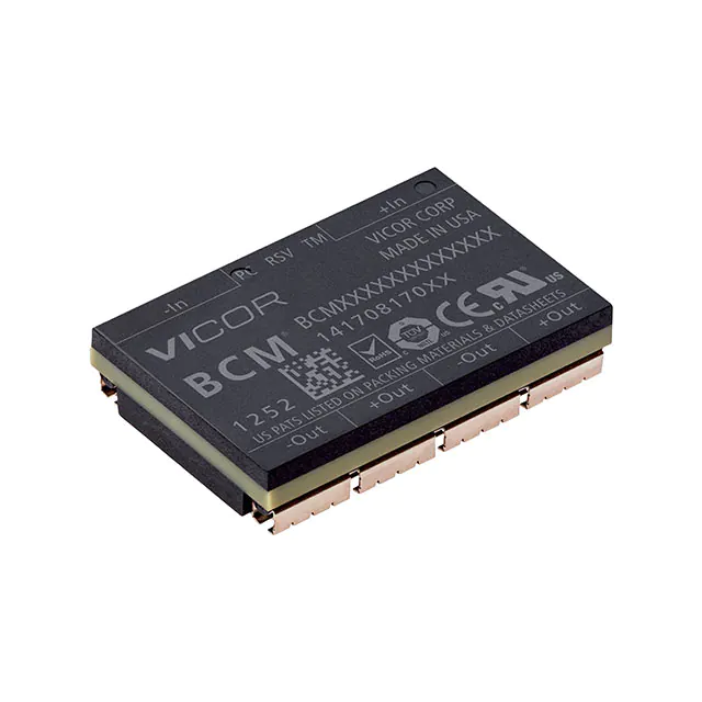
The MBCM270F338M235A00 is provided in a VI Chip package
compatible with standard pick-and-place and surface mount
assembly processes.
• Provides enable/disable control,
internal temperature monitoring
Part Numbering
• Can be paralleled to create multi-kW arrays
Product Number
MBCM270x450M270A00
Typical Applications
Package Style (x)
F = J-Lead
T = Through hole
Product Grade
M = -55° to 125°C
For Storage and Operating Temperatures see General Characteristics.
• High Voltage 270V Aircraft Distributed Power
• 28VDC MIL-COTS PRM™ Interface (MP028F036M21AL)
• High Density Power Supplies
• Communications Systems
Typical Application
VC
SG
OS
CD
PR
PC
TM
enable / disable
switch
BCM
SW1
F1
VIN
BCM® Bus Converter
Page 1 of 23
C1
PC
TM
IL
VC
PC
TM
PRM
VTM
+IN
+OUT
+IN
+OUT
+IN
+OUT
-IN
-OUT
-IN
-OUT
-IN
-OUT
1 µF
Rev 1.8
08/2016
vicorpower.com
800 927.9474
L
O
A
D
�MBCM270x338M235A00
Pin Configuration
4
3
2
A
A
+OUT
1
B
B
C
C
D
D
E
E
F
-OUT
G
H
H
J
J
K
K
+OUT
-OUT
+IN
L
L
M
M
N
N
P
P
R
R
TM
RSV
PC
-IN
T
T
Bottom View
Pin Descriptions
Pin Number
Signal Name
Type
Function
A1-E1, A2-E2
+IN
INPUT POWER
Positive input power terminal
L1-T1, L2-T2
–IN
INPUT POWER
RETURN
Negative input power terminal
H1, H2
TM
OUTPUT
J1, J2
RSV
NC
Temperature monitor, input side referenced signal
No connect
K1, K2
PC
OUTPUT/INPUT
A3-D3, A4-D4,
J3-M3, J4-M4
Enable and disable control, input side referenced signal
+OUT
OUTPUT POWER
Positive output power terminal
E3-H3, E4-H4,
N3-T3, N4-T4
–OUT
OUTPUT POWER
RETURN
Negative output power terminal
Control Pin Specifications
See Using the Control Signals PC, TM for more information.
PC (BCM Primary Control)
TM (BCM Temperature Monitor)
The PC pin can enable and disable the BCM module. When held
below VPC_DIS the BCM shall be disabled. When allowed to
float with an impedance to –IN of greater than 50kΩ the
module will start. When connected to another BCM PC pin
the BCM modules will start simultaneously when enabled. The PC
pin is capable of being driven high either by an external logic signal
or internal pull up to 5V (operating).
The TM pin monitors the internal temperature of the BCM module
within an accuracy of ±5°C. It has a room temperature setpoint of
~3.0V and an approximate gain of 10mV/°C. It can source up to
100µA and may also be used as a “Power Good” flag to verify that
the BCM module is operating.
BCM® Bus Converter
Page 2 of 23
Rev 1.8
08/2016
vicorpower.com
800 927.9474
�MBCM270x338M235A00
Absolute Maximum Voltage Ratings
The absolute maximum ratings below are stress ratings only. Operation at or beyond these maximum ratings can cause permanent damage to the device.
Parameter
Comments
Min
Max
Unit
+IN to –IN
-1.0
400
VDC
PC to –IN
-0.3
20
VDC
TM to –IN
-0.3
7
VDC
+IN/–IN to +OUT/–OUT
Isolation voltage (hipot)
4242
V
+IN/–IN to +OUT/–OUT
Working voltage (IN - OUT)
500
V
60
VDC
245
°C
+OUT to –OUT
Temperature during reflow
BCM® Bus Converter
Page 3 of 23
-1.0
MSL 4 (Datecode 1528 and later)
Rev 1.8
08/2016
vicorpower.com
800 927.9474
�MBCM270x338M235A00
Electrical Specifications
Specifications apply over all line and load conditions, unless otherwise noted; boldface specifications apply over the temperature range of
-55°C ≤ TJ ≤ 125°C (M-Grade); all other specifications are at TJ = 25ºC unless otherwise noted.
Attribute
Symbol
Conditions / Notes
Min
Typ
Max
Unit
240
270
330
VDC
1
V/µs
410
mW
10
W
4
A
0.95
A
Powertrain
Voltage range
dV/dt
VIN
dVIN /dt
Quiescent power
PQ
PC connected to -IN
No load power dissipation
PNL
VIN = 240 to 330V
395
Inrush Current Peak
IINR_P
VIN = 330V COUT = 100μF, POUT = 235W
DC Input Current
IIN_DC
POUT = 235W
K Factor
( )
VOUT
VIN
Output Power (Average)
2.5
K
POUT
1/8
VIN = 270VDC
235
VIN = 240 – 330VDC
215
Output Power (Peak)
POUT_P
VIN = 270 VDC, Average POUT < = 235W, Tpeak < 5ms
Output Voltage
VOUT
No Load
Output Current (Average)
IOUT
POUT < = 235W
30
VIN = 270V, POUT = 235W
94.1
95.4
94
95.2
93.7
94.7
Efficiency (Ambient)
h
Efficiency (Hot)
h
VIN = 270V, TJ = 100°C, POUT = 235W
Minimum Efficiency
(Over Load Range)
h
60W < POUT < 235W Max
90
VIN = 240V to 330V, POUT = 235W
W
352.5
W
41.25
V
7.3
A
%
%
%
Output Resistance (Ambient)
ROUT
TJ = 25°C
100
130
170
mΩ
Output Resistance (Hot)
ROUT
TJ = 125°C
130
180
210
mΩ
Output Resistance (Cold)
ROUT
TJ = -55°C
40
105
160
mΩ
Load Capacitance
COUT
100
µF
Switching Frequency
FSW
1.56
1.64
1.72
MHz
Ripple Frequency
FSW_RP
3.12
3.28
3.44
MHz
Output Voltage Ripple
VOUT_PP
160
400
mV
540
620
ms
VIN to VOUT (Application of VIN)
BCM® Bus Converter
Page 4 of 23
TON1
COUT = 0μF, POUT = 235W, VIN = 270V
VIN = 270V, CPC = 0
Rev 1.8
08/2016
460
vicorpower.com
800 927.9474
�MBCM270x338M235A00
Electrical Specifications
Specifications apply over all line and load conditions, unless otherwise noted; boldface specifications apply over the temperature range of
-55°C ≤ TJ ≤ 125°C (M-Grade); all other specifications are at TJ = 25ºC unless otherwise noted.
Attribute
Symbol
Conditions / Notes
Min
Typ
Max
Unit
Protection
Input overvoltage recovery threshold
VIN_OVLO-
350
365
380
V
Input overvoltage lockout threshold
VIN_OVLO+
355
372
385
V
Input undervoltage lockout
threshold
VIN_UVLO-
90
115
125
V
Input undervoltage recovery threshold
VIN_UVLO+
100
125
135
V
9
12
14
A
Output overcurrent trip
IOCP
Short circuit protection trip threshold
ISCP
14
Short circuit protection response time
constant
TSCP
0.8
1
1.2
µs
TJ_OTP
125
130
135
°C
Thermal shutdown threshold
VIN = 270V, 25°C
A
400
350
Output Power (W)
300
250
200
150
100
50
0
29.00
31.00
33.00
35.00
Steady State
37.00
5ms 352.5W Ave
Figure 1 — Safe operating area
BCM® Bus Converter
Page 5 of 23
Rev 1.8
08/2016
vicorpower.com
800 927.9474
39.00
41.00
�MBCM270x338M235A00
Signal Characteristics
Specifications apply over all line and load conditions, unless otherwise noted; boldface specifications apply over the temperature range of
-55°C ≤ TJ ≤ 125°C (M-Grade); all other specifications are at TJ = 25ºC unless otherwise noted.
Primary Control: PC
• The PC pin enables and disables the BCM. When held low, the BCM module is disabled.
• In an array of BCM modules, PC pins should be interconnected to synchronize start up and permit start up into full load conditions.
• PC pin outputs 5V during normal operation. PC pin internal bias level drops to 2.5V during fault mode, provided VIN remains
in the valid range.
Attribute
Symbol
Conditions / Notes
Min
Typ
Max
Unit
VPC
4.7
5
5.3
V
PC Voltage (Enable)
VPC_EN
2
2.5
3
V
PC Voltage (Disable)
VPC_DIS
1.95
V
PC Source Current (Startup)
IPC_EN
50
100
300
µA
PC Source Current (Operating)
IPC_OP
2
3.5
5
mA
50
150
400
kΩ
1000
pF
1000
pF
PC Voltage (Operating)
PC Internal Resistance
RPC_SNK
PC Capacitance (Internal)
CPC_INT
PC Capacitance (External)
CPC_EXT
External PC Resistance
RPC
PC External Toggle Rate
FPC_TOG
PC to VOUT with PC Released
PC to VOUT, Disable PC
Internal pull down resistor
External capacitance delays PC enable time
50
Connected to –VIN
TON2
VIN = 270V, Pre-applied, CPC = 0, COUT = 0
TPC_DIS
VIN = 270V, Pre-applied, CPC = 0, COUT = 0
50
kΩ
1
Hz
100
150
µs
4
10
µs
Typ
Max
Unit
+5
°C
Temperature Monitor: TM
• The TM pin monitors the internal temperature of the controller IC within an accuracy of ±5°C.
• Can be used as a “Power Good” flag to verify that the BCM module is operating.
• Is used to drive the internal comparator for Overtemperature Shutdown.
Attribute
Symbol
TM accuracy
ACTM
TM Gain
ATM
TM Source Current
ITM
TM Internal Resistance
External TM Capacitance
TM Voltage Ripple
Conditions / Notes
Min
-5
10
25
RTM_SNK
CTM
VTM_PP
CTM = 0μF, VIN = 330V, POUT = 235W
200
Reserved: RSV
Reserved for factory use. No connection should be made to this pin.
BCM® Bus Converter
Page 6 of 23
40
Rev 1.8
08/2016
vicorpower.com
800 927.9474
400
mV/ °C
100
µA
50
kΩ
50
pF
500
mV
�BCM® Bus Converter
Page 7 of 23
NL
5V
2.5 V
5V
3V
PC
VUVLO+
VUVLO–
Rev 1.8
08/2016
vicorpower.com
800 927.9474
1
A
E: TON2
F: TOCP
G: TPC–DIS
H: TSCP**
B
D
1: Controller start
2: Controller turn off
3: PC release
C
*Min value switching off
**From detection of error to power train shut down
A: TON1
B: TOVLO*
C: TAUTO_RESTART
D:TUVLO
0.4 V
3 V @ 27°C
TM
LL • K
VOUT
C
500mS
before retrial
3V
VIN
VOVLO+
VOVLO–
2
F
4: PC pulled low
5: PC released on output SC
6: SC removed
IOCP
ISSP
IOUT
E
3
G
4
Notes:
H
5
– Timing and signal amplitudes are not to scale
– Error pulse width is load dependent
6
MBCM270x338M235A00
Timing Diagram
�MBCM270x338M235A00
Applications Characteristics
All specifications are at TJ = 25ºC unless otherwise noted. See associated figures for general trend data.
Attribute
Symbol
Conditions / Notes
Min
Typ
Max
Unit
No Load Power
PNL
VIN = 270V, PC enabled
5.5
W
Inrush Current Peak
INR_P
COUT = 100μF, POUT = 235W
2.5
A
Efficiency (Ambient)
η
VIN = 270V, POUT = 235W
95.4
%
Efficiency (Hot – 100°C)
η
VIN = 270V, POUT = 235W
94.7
%
Output Resistance (-55°C)
ROUT
VIN = 270V
105
mΩ
Output Resistance (25°C)
ROUT
VIN = 270V
130
mΩ
Output Resistance (120°C)
ROUT
VIN = 270V
180
mΩ
COUT = 0μF, POUT = 235W @ VIN = 270,
VIN = 270V
160
mV
Output Voltage Ripple
VOUT_PP
VOUT Transient (Positive)
VOUT_TRAN+
IOUT_STEP = 0 TO 7.3A, ISLEW >10A/μs
1.4
V
VOUT Transient (Negative)
VOUT_TRAN
IOUT_STEP = 7.3A to 0A, ISLEW > 10A/μs
1.3
V
150
µs
5
ms
120
µs
3
V
Undervoltage Lockout
Response Time
TUVLO
Output Overcurrent
Response Time
TOCP
Overvoltage Lockout
Response Time
TOVLO
TM Voltage (Ambient)
BCM® Bus Converter
Page 8 of 23
VTM_AMB
9 < IOCP < 14A
TJ ≅ 27°C
Rev 1.8
08/2016
vicorpower.com
800 927.9474
�MBCM270x338M235A00
Application Characteristics
9
96.0
8
95.8
7
95.6
6
Efficiency (%)
No Load Power Dissipation (W)
The following values, typical of an application environment, are collected at TCASE = 25ºC unless otherwise noted. See associated figures for general trend
data.
5
4
3
2
95.2
95.0
94.8
94.6
94.4
1
0
95.4
94.2
230
250
270
290
310
-100
330
-50
Input Voltage (V)
-55°C
TCASE:
25°C
V IN:
100°C
Power Dissipation (W)
96
Efficiency (%)
95
90
85
80
75
70
100
150
240V
270V
330V
15
13
11
9
7
5
65
0
1
2
3
4
5
6
7
0
8
1
240V
270V
2
3
4
5
6
7
8
7
8
Output Current (A)
Output Current (A)
VIN:
240V
VIN:
330V
270V
330V
Figure 5 — Power dissipation at TCASE = -55°C
Figure 4 — Efficiency at TCASE = -55°C
98
15
Power Dissipation (W)
96
Efficiency (%)
50
Figure 3 — Full load efficiency vs. temperature; VIN
Figure 2 — No load power dissipation vs. VIN; TCASE
94
92
90
88
86
84
82
80
0
Case Temperature (C)
13
11
9
7
5
3
0
1
2
VIN:
3
4
5
Output Current (A)
240V
270V
6
330V
Figure 6 — Efficiency at TCASE = 25°C
BCM® Bus Converter
Page 9 of 23
7
8
0
1
2
VIN:
3
4
5
Output Current (A)
240V
270V
Figure 7 — Power dissipation at TCASE = 25°C
Rev 1.8
08/2016
vicorpower.com
800 927.9474
6
330V
�MBCM270x338M235A00
Application Characteristics (Cont.)
98
Power Dissipation (W)
96
Efficiency (%)
94
92
90
88
86
84
82
80
16.5
14.5
12.5
10.5
8.5
6.5
4.5
2.5
0
1
2
3
4
5
6
7
8
0
1
270V
6
7
8
270V
7
8
330V
180
180
160
170
140
Ripple (mV pk-pk)
�ROUT (mΩ)
5
Figure 9 — Power dissipation at TCASE = 100°C
190
160
150
140
130
120
100
120
100
80
60
40
20
100
90
-80
4
240V
VIN:
330V
Figure 8 — Efficiency at TCASE = 100°C
3
Output Current (A)
Output Current (A)
240V
VIN:
2
-60
-40
-20
0
20
40
60
80
Case Temperature (°C)
I OUT :
0.73A
120
0
0
1
Rev 1.8
08/2016
2
3
4
5
6
Load Current (A)
7.3A
Figure 10 — ROUT vs. temperature; nominal input
BCM® Bus Converter
Page 10 of 23
100
VIN:
270V
Figure 11 — VRIPPLE vs. IOUT; no external COUT. Board mounted
module, scope setting: 20MHz analog BW
vicorpower.com
800 927.9474
�MBCM270x338M235A00
Application Characteristics (Cont.)
Figure 12 — Start up from applicaiton of PC; VIN preapplied COUT
Figure 13 — Start up from applicaiton of VIN
Figure 14 — Full load ripple, 100µF CIN ; no external COUT. Board
mounted module, scope setting: 20MHz analog BW
Figure 15 — 0A - 7.3A transient response. CIN = 100µF,
no external COUT
Figure 16 — 7.3A - 0A transient response. CIN = 100µF,
no external COUT
Figure 17 — PC disable waveform, 270VIN, 100μF COUT full load
BCM® Bus Converter
Page 11 of 23
Rev 1.8
08/2016
vicorpower.com
800 927.9474
�MBCM270x338M235A00
Application Characteristics (Cont.)
400
350
50 mS operation
full current
Input Voltage (V)
330
300
OVP
Normal
Operating Range
280
MIL-STD-704F Envelope of normal
V transients for 270 Vdc systems
250
200
50% rated current
50 mS full current 1% duty
150
125
UVL
0
20
40
60
80
Duration (ms)
Figure 18 — Envelope of normal voltage transient for 270Vdc system.
BCM® Bus Converter
Page 12 of 23
Rev 1.8
08/2016
vicorpower.com
800 927.9474
100
120
�MBCM270x338M235A00
General Characteristics
Specifications apply over all line and load conditions, unless otherwise noted; boldface specifications apply over the temperature range of
-55°C ≤ TJ ≤ 125°C (M-Grade); all other specifications are at TJ = 25ºC unless otherwise noted.
Attribute
Symbol
Conditions / Notes
Min
Typ
Max
Unit
Mechanical
Length
L
32.4 / [1.27]
32.5 / [1.28]
32.6 / [1.29]
mm / [in]
Width
W
21.7 / [0.85]
22.0 / [0.87]
22.3 / [0.89]
mm / [in]
Height
H
6.48 / [0.255]
6.73 / [0.265] 6.98 / [0.275]
mm / [in]
Volume
Vol
No heat sink
4.81 / [0.295]
cm3/ [in3]
Footprint
F
No heat sink
7.3 / [1.1]
cm2/ [in2]
Power Density
PD
No heat sink
796
W/in3
49
W/cm3
Weight
W
14 / [0.5]
g / [oz]
Nickel (0.51-2.03μm)
Lead Finish
µm
Palladium (0.02-0.15μm)
Gold (0.003-0.05μm)
Thermal
Operating temperature
TJ
-55
125
°C
Storage Temperature
TST
-65
125
°C
Thermal Impedance
ØJC
1.5
°C/W
Min Board Heat sinking
1.1
Thermal Capacity
9
Ws/°C
Assembly
Peak Compressive Force
Applied to Case (Z-axis)
No J-lead support
ESDHBM
ESD Rating
ESDMM
5
Human Body Model,
JEDEC JESD 22-A114c.01
1500
Machine Model,
JEDEC JESD 22-A115-A
400
6
lbs
VDC
Soldering
Peak Temperature During Reflow
MSL 4 (Datecode 1528 and later)
Peak Time Above 183°C
245
°C
150
s
Peak Heating Rate During Reflow
1.5
3
°C/s
Peak Cooling Rate Post Reflow
1.5
6
°C/s
500
V
800
pF
Safety
Working voltage (IN – OUT)
VWORKING
Isolation voltage (hipot)
VHIPOT
Isolation capacitance
CIN_OUT
Isolation resistance
RIN_OUT
MTBF
4242
Unpowered unit
500
V
660
10
MIL HDBK 217F, 25°C, GB
MΩ
4.2
cTUVus
Agency approvals / standards
cURus
CE Marked for Low Voltage Directive and ROHS recast directive, as applicable.
BCM® Bus Converter
Page 13 of 23
Rev 1.8
08/2016
vicorpower.com
800 927.9474
MHrs
�MBCM270x338M235A00
Using the Control Signals PC, TM
Primary Control (PC) pin can be used to accomplish the following
functions:
n Logic enable and disable for module: Once TON1 time has
been satisfied, a PC voltage greater than VPC_EN will cause
the module to start. Bringing PC lower than VPC_DIS will
cause the module to enter standby.
n Auxiliary voltage source: Once enabled in regular
operational conditions (no fault), each BCM module
PC provides a regulated 5V, 3.5mA voltage source.
n Synchronized start up: In an array of parallel modules, PC
pins should be connected to synchronize start up across
units. This permits the maximum load and capacitance
to scale by the number of paralleled modules.
n Output disable: PC pin can be actively pulled down in order
to disable the module. Pull down impedance shall be lower
than 60Ω.
n Fault detection flag: The PC 5V voltage source is internally
turned off as soon as a fault is detected.
n Note that PC can not sink significant current during a fault
condition. The PC pin of a faulted module will not cause
interconnected PC pins of other modules to be disabled.
Temperature Monitor (TM) pin provides a voltage proportional
to the absolute temperature of the converter control IC.
It can be used to accomplish the following functions:
n Monitor the control IC temperature: The temperature in
Kelvin is equal to the voltage on the TM pin scaled
by 100. (i.e. 3.0V = 300K = 27ºC). If a heat sink is applied,
TM can be used to protect the system thermally.
n Fault detection flag: The TM voltage source is internally
turned off as soon as a fault is detected. For system
monitoring purposes microcontroller interface faults are
detected on falling edges of TM signal.
BCM® Bus Converter
Page 14 of 23
Rev 1.8
08/2016
vicorpower.com
800 927.9474
�MBCM270x338M235A00
Sine Amplitude Converter™ Point of Load Conversion
IIN
IOUT
ROUT
+
+
K • IOUT
VIN
IQ
V•I
+
+
–
K
K • VIN
VOUT
–
–
–
Figure 19 — BCM® DC model
The Sine Amplitude Converter (SAC™) uses a high frequency
resonant tank to move energy from input to output. The resonant
LC tank, operated at high frequency, is amplitude modulated as
a function of input voltage and output current. A small amount
of capacitance embedded in the input and output stages of the
module is sufficient for full functionality and is key to achieving
power density.
the SAC control, gate drive circuitry, and core losses.
The use of DC voltage transformation provides additional
interesting attributes. Assuming that ROUT = 0Ω and IQ = 0A, Eq. (3)
now becomes Eq. (1) and is essentially load independent, resistor R
is now placed in series with VIN.
The MBCM270x338M235A00 SAC can be simplified into the
preceeding model.
R
SAC
SAC
1/8
KK==1/32
TM
At no load:
VVin
in
VOUT = VIN • K
+
–
(1)
K represents the “turns ratio” of the SAC.
Rearranging Eq (1):
Figure 20 — K = 1/8 Sine Amplitude Converter™
with series input resistor
VOUT (2)
K =
VIN
In the presence of load, VOUT is represented by:
VOUT = VIN • K – IOUT • ROUT (3)
The relationship between VIN and VOUT becomes:
VOUT = (VIN – IIN • R) • K
(5)
Substituting the simplified version of Eq. (4)
(IQ is assumed = 0A) into Eq. (5) yields:
VOUT = VIN • K – IOUT • R • K2 (6)
and IOUT is represented by:
IIN – IQ (4)
IOUT =
K
ROUT represents the impedance of the SAC, and is a function of the
RDSON of the input and output MOSFETs and the winding resistance
of the power transformer. IQ represents the quiescent current of
BCM® Bus Converter
Page 15 of 23
V
Vout
out
Rev 1.8
08/2016
vicorpower.com
800 927.9474
�MBCM270x338M235A00
This is similar in form to Eq. (3), where ROUT is used to represent
the characteristic impedance of the SACtm. However, in this case a
real R on the input side of the SAC is effectively scaled by K 2 with
respect to the output.
Assuming that R = 1Ω, the effective R as seen from the output side
is 15.6mΩ, with K = 1/8 as shown in Figure 20.
A similar exercise should be performed with the additon of a
capacitor or shunt impedance at the input to the SAC.
A switch in series with VIN is added to the circuit. This is depicted in
Figure 21.
Low impedance is a key requirement for powering a highcurrent, low-voltage load efficiently. A switching regulation stage
should have minimal impedance while simultaneously providing
appropriate filtering for any switched current. The use of a SAC
between the regulation stage and the point of load provides a
dual benefit of scaling down series impedance leading back to
the source and scaling up shunt capacitance or energy storage
as a function of its K factor squared. However, the benefits are
not useful if the series impedance of the SAC is too high. The
impedance of the SAC must be low, i.e. well beyond the crossover
frequency of the system.
A solution for keeping the impedance of the SAC low involves
switching at a high frequency. This enables small magnetic
components because magnetizing currents remain low. Small
magnetics mean small path lengths for turns. Use of low loss core
material at high frequencies also reduces core losses.
S
VVin
in
+
–
C
The two main terms of power loss in the BCM module are:
SAC™
SAC
1/8
KK==1/32
Vout
V
out
n No load power dissipation (PNL): defined as the power
used to power up the module with an enabled powertrain
at no load.
n Resistive loss (PROUT): refers to the power loss across
the BCM module modeled as pure resistive impedance.
Figure 21 — Sine Amplitude Converter™ with input capacitor
A change in VIN with the switch closed would result in a change in
capacitor current according to the following equation:
PDISSIPATED = PNL + PR (10)
OUT
Therefore,
IC(t) = C
dVIN (7)
dt
Assume that with the capacitor charged to VIN, the switch is
opened and the capacitor is discharged through the idealized SAC.
In this case,
POUT = PIN – PDISSIPATED = PIN – PNL – PR (11)
OUT
The above relations can be combined to calculate the overall
module efficiency:
POUT PIN – PNL – PROUT
h =
=
P
P
IC = IOUT • K
(8)
IN
IN
substituting Eq. (1) and (8) into Eq. (7) reveals:
= VIN • IIN – PNL – (IOUT)2 • ROUT
VIN • IIN
C dVOUT (9)
IOUT =
•
K2 dt
= 1 –
(PNL + (IOUT)2 • ROUT)
VIN • IIN
The equation in terms of the output has yielded a K 2 scaling factor
for C, specified in the denominator of the equation.
A K factor less than unity results in an effectively larger capacitance
on the output when expressed in terms of the input. With a
K = 1/8 as shown in Figure 21, C = 1µF would appear as C = 64µF
when viewed from the output.
BCM® Bus Converter
Page 16 of 23
Rev 1.8
08/2016
vicorpower.com
800 927.9474
(12)
�MBCM270x338M235A00
Input and Output Filter Design
A major advantage of SAC™ systems versus conventional PWM
converters is that the transformers do not require large
functional filters. The resonant LC tank, operated at extreme high
frequency, is amplitude modulated as a function of input voltage
and output current and efficiently transfers charge through the
isolation transformer. A small amount of capacitance embedded
in the input and output stages of the module is sufficient for full
functionality and is key to achieve power density.
This paradigm shift requires system design to carefully evaluate
external filters in order to:
1. Guarantee low source impedance:
To take full advantage of the BCM module’s dynamic
response, the impedance presented to its input terminals
must be low from DC to approximately 5MHz. The
connection of the bus converter module to its power
source should be implemented with minimal distribution
inductance. If the interconnect inductance exceeds
100nH, the input should be bypassed with a RC damper
to retain low source impedance and stable operation.
With an interconnect inductance of 200nH, the RC damper
may be as high as 1µF in series with 0.3Ω. A single
electrolytic or equivalent low-Q capacitor may be used in
place of the series RC bypass.
2. Further reduce input and/or output voltage ripple
without sacrificing dynamic response:
Given the wide bandwidth of the module, the source
response is generally the limiting factor in the overall
system response. Anomalies in the response of the source
will appear at the output of the module multiplied by its
K factor.
Within this frequency range, capacitance at the input appears as
effective capacitance on the output per the relationship
defined in Eq. 13.
C
COUT = IN
K2
This enables a reduction in the size and number of capacitors used
in a typical system.
Thermal Considerations
VI Chip® products are multi-chip modules whose temperature
distribution varies greatly for each part number as well as with the
input / output conditions, thermal management and environmental
conditions. Maintaining the top of the MBCM270x338M235A00
case to less than 100ºC will keep all junctions within the VI Chip
module below 125ºC for most applications.
The percent of total heat dissipated through the top surface
versus through the J-lead is entirely dependent on the particular
mechanical and thermal environment. The heat dissipated through
the top surface is typically 60%. The heat dissipated through the
J-lead onto the PCB surface is typically 40%. Use 100% top surface
dissipation when designing for a conservative cooling solution.
It is not recommended to use a VI Chip module for an extended
period of time at full load without proper heat sinking.
3. Protect the module from overvoltage transients imposed
by the system that would exceed maximum ratings and
cause failures:
The module input/output voltage ranges shall not be
exceeded. An internal overvoltage lockout function
prevents operation outside of the normal operating input
range. Even during this condition, the powertrain is
exposed to the applied voltage and power MOSFETs must
withstand it. A criterion for protection is the maximum
amount of energy that the input or output switches can
tolerate if avalanched.
Total load capacitance at the output of the BCM module shall not
exceed the specified maximum. Owing to the wide bandwidth
and low output impedance of the module, low-frequency bypass
capacitance and significant energy storage may be more densely
and efficiently provided by adding capacitance at the input of
the module. At frequencies