Not Recommended For New Designs
NBM™ in
a VIA™ Package
Bus Converter
NBM3814x46C15A6yzz
®
S
US
C
C
NRTL
US
Non-Isolated, Fixed-Ratio DC-DC Converter
Features & Benefits
Product Ratings
• Up to 160A continuous low-voltage-side current
• Fixed transformation ratio (K) of 1/3
• Up to
1258W/in3
power density
• 97.9% peak efficiency
VHI = 42V (36 – 46V)
ILO = up to 160A
VLO = 14V (12 – 15.3V)
(no load)
K = 1/3
Product Description
• Bidirectional operation capability
The NBM3814x46C15A6yzz in a VIA package is a high-efficiency
Bus Converter, operating from a 36 to 46VDC high-voltage bus to
deliver a non‑isolated 12 to 15.3VDC unregulated, low voltage.
• Integrated ceramic capacitance filtering
• Parallel operation for multi-kW arrays
This unique, ultra-low-profile module incorporates
DC‑DC conversion and integrated filtering in a chassis- or
PCB‑mount form factor.
• OV, OC, UV, short circuit and thermal protection
• 3814 package
The NBM offers low noise, fast transient response and
industry‑leading efficiency and power density.
• High MTBF
• Thermally enhanced VIA package
Leveraging the thermal and density benefits of Vicor VIA packaging
technology, the NBM module offers flexible thermal management
options with very low top and bottom side thermal impedances.
Typical Applications
When combined with downstream Vicor DC-DC conversion
components and regulators, the NBM allows the Power Design
Engineer to employ a simple, low-profile design, which will
differentiate the end system without compromising on cost or
performance metrics.
• DC Power Distribution
• Information and Communication
Technology (ICT) Equipment
• High-End Computing Systems
The NBM non-isolated topology allows start up and steady
state operation in forward and reverse directions. It provides
bidirectional protections. However if the powertrain is disabled
by any protection and VLO is present, then a voltage equal to VLO
minus two diode drops will appear on the high-voltage side.
• Automated Test Equipment
• Industrial Systems
• High-Density
Energy Systems
• Transportation
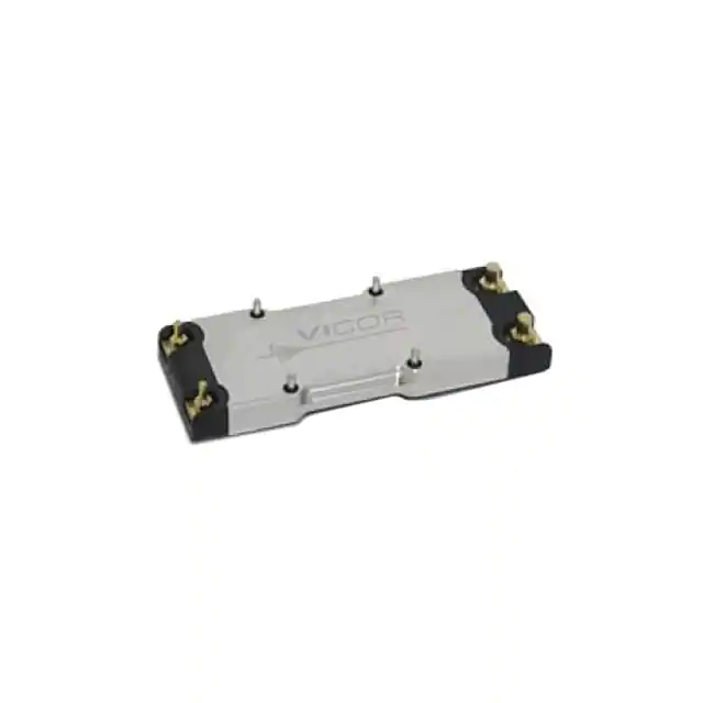
Size:
3.76 x 1.40 x 0.37in
[95.59 x 35.54 x 9.40mm]
Part Ordering Information
Product
Function
Package
Length
Package
Width
Package
Type
NBM
38
14
x
NBM =
Non-Isolated
Bus Converter
Module
Length in
Inches x 10
Width in
Inches x 10
B = Board VIA
V = Chassis VIA
[a]
High-Side
Max
Max
Max
Voltage
Product Grade
High‑Side
Low‑Side Low‑Side
Range
(Case Temperature)
Voltage
Voltage Current
Ratio
46
C
15
Internal Reference
High-Temperature Current Derating may apply; See Figure 1, specified thermal operating area.
NBM™ in a VIA™ Package
Page 1 of 25
Rev 1.6
08/2018
A6
Option Field
y
zz
C = –20 to 100°C [a]
T = –40 to 100°C [a]
00 = Chassis/Always On
04 = Short Pin/Always On
08 = Long Pin/Always On
�NBM3814x46C15A6yzz
Not Recommended For New Designs
Typical Applications
NBM in a VIA Package
FUSE
+HI
+LO
LO
Side
HI
Side
V
HI
V
PGND
PoL
LO
NBM3814x46C15A6yzz at point-of-load providing fixed ratio step-down DC–DC conversion to PoL devices.
NBM is operating in forward direction.
NBM in a VIA Package
FUSE
+HI
+LO
LO
Side
HI
Side
LOAD
V
PGND
HI
NBM3814x46C15A6yzz providing fixed ratio step-up DC-DC conversion. NBM is operating in reverse direction.
NBM™ in a VIA™ Package
Page 2 of 25
Rev 1.6
08/2018
V
LO
�NBM3814x46C15A6yzz
Not Recommended For New Designs
Pin Configuration
10
1
TOP VIEW
12
3
+HI
PGND
PGND
+LO
+HI
PGND
PGND
+LO
2
11
13
4
2
11
13
4
NBM3814 in a VIA Package - Chassis (Lug) Mount
TOP VIEW
+HI
PGND
PGND
+LO
+HI
PGND
PGND
+LO
10
12
1
3
NBM3814 in a VIA Package - Board (PCB) Mount
Pin Descriptions
Pin Number
Signal Name
Type
1, 2
+HI
HIGH SIDE POWER
High-voltage-side positive power terminal
3, 4
+LO
LOW SIDE POWER
Low-voltage-side positive power terminal
10, 11, 12, 13
PGND
POWER RETURN
NBM™ in a VIA™ Package
Page 3 of 25
Function
Common negative power terminal
Rev 1.6
08/2018
�Not Recommended For New Designs
NBM3814x46C15A6yzz
Absolute Maximum Ratings
The absolute maximum ratings below are stress ratings only. Operation at or beyond these maximum ratings can cause permanent damage to the device.
Parameter
Comments
+HI to PGND
Min
Max
Unit
–1
60
V
1
V/µs
HI_DC or LO_DC Slew Rate
+LO to PGND
Isolation Voltage /
Dielectric Withstand [b]
[b]
–1
20
V
High-voltage side to case
N/A
VDC
High-voltage side to low-voltage side
N/A
VDC
Low-voltage side to case
N/A
VDC
The PGND of the NBM in a VIA package is directly connected to the case. The NBM does not contain any insulation (isolation) from high-voltage side to
low-voltage side
NBM™ in a VIA™ Package
Page 4 of 25
Rev 1.6
08/2018
�Not Recommended For New Designs
NBM3814x46C15A6yzz
Electrical Specifications
Specifications apply over all line and load conditions, unless otherwise noted; boldface specifications apply over the temperature range of
–40°C ≤ TCASE ≤ 100°C (T-Grade); all other specifications are at TCASE = 25ºC unless otherwise noted.
Attribute
Symbol
Conditions / Notes
Min
Typ
Max
Unit
46
V
15
V
General Powertrain Specification – Forward Direction Operation (High-Voltage Side to Low-Voltage Side)
HI-Side Voltage Range,
(Continuous)
VHI_DC
HI-Side Voltage
Initialization Threshold
VµC_ACTIVE
HI-Side Quiescent Current
IHI_Q
36
HI-side voltage where internal controller is initialized,
(powertrain inactive)
Disabled, VHI_DC = 42V
8
TCASE ≤ 100ºC
12
VHI_DC = 42V, TCASE = 25ºC
No-Load Power Dissipation
HI-Side Inrush Current Peak
PHI_NL
IHI_INR_PK
12.5
5
VHI_DC = 42V
28
22
VHI_DC = 36 – 46V
31
30
TCASE ≤ 100ºC
DC HI-Side Current
Transformation Ratio
LO-Side Current (Continuous)
LO-Side Current (Pulsed)
Efficiency (Ambient)
IHI_IN_DC
K
ILO_OUT_DC
ILO_OUT_PULSE
ηAMB
19.5
VHI_DC = 36 – 46V, TCASE = 25 ºC
VHI_DC = 46V, CLO_EXT = 3000μF,
RLOAD_LO = 20% of full-load current
A
At ILO_OUT_DC = 160A, TCASE ≤ 85ºC
53.9
High voltage to low voltage,
K = VLO_DC / VHI_DC, at no load
1/3
TCASE ≤ 85°C
160
A
10ms pulse, 25% duty cycle,
ILO_OUT_AVG ≤ 50% rated ILO_OUT_DC
176
A
VHI_DC = 42V, ILO_OUT_DC = 160A
96.8
97.6
VHI_DC = 36V to 46V, ILO_OUT_DC = 160A
96.5
VHI_DC = 42V, ILO_OUT_DC = 80A
97.3
97.8
96.7
97.1
%
VHI_DC = 42V, ILO_OUT_DC = 160A, TCASE = 85°C
Efficiency (Over Load Range)
η20%
32A < ILO_OUT_DC < 160A
95
RLO_COLD
VHI_DC = 42V, ILO_OUT_DC = 160A, TCASE = –40°C
0.8
1.3
1.7
RLO_AMB
VHI_DC = 42V, ILO_OUT_DC = 160A
0.9
1.7
2.1
RLO_HOT
VHI_DC = 42V, ILO_OUT_DC = 160A, TCASE = 85°C
1.5
2.1
2.4
LO-side voltage ripple frequency = 2x FSW
1.14
1.20
1.26
LO-Side Voltage Ripple
FSW
VLO_OUT_PP
CLO_EXT = 0μF, ILO_OUT_DC = 160A,
VHI_DC = 42V, 20MHz BW
TCASE ≤ 100ºC
NBM™ in a VIA™ Package
Page 5 of 25
A
V/V
ηHOT
Switching Frequency
W
75
Efficiency (Hot)
LO-Side Output Resistance
mA
%
%
110
MHz
mV
205
Rev 1.6
08/2018
mΩ
�Not Recommended For New Designs
NBM3814x46C15A6yzz
Electrical Specifications (Cont.)
Specifications apply over all line and load conditions, unless otherwise noted; boldface specifications apply over the temperature range of
–40°C ≤ TCASE ≤ 100°C (T-Grade); all other specifications are at TCASE = 25ºC unless otherwise noted.
Attribute
Symbol
Conditions / Notes
Min
Typ
Max
Unit
General Powertrain Specification – Forward Direction Operation (High-Voltage Side to Low-Voltage Side), Cont.
Effective HI-side Capacitance
(Internal)
CHI_INT
Effective value at 42VHI_DC
16.8
µF
Effective LO-Side Capacitance
(Internal)
CLO_INT
Effective value at 14VLO_DC
140
µF
Rated LO-Side Capacitance
(External)
CLO_OUT_EXT
Excessive capacitance may drive module into short
circuit protection
Rated LO-Side Capacitance
(External), Parallel Array Operation
CLO_OUT_AEXT
CLO_OUT_AEXT Max = N • 0.5 • CLO_OUT_EXT MAX, where
N = the number of units in parallel
3000
µF
Powertrain Protection Specification – Forward Direction Operation (High-Voltage Side to Low-Voltage Side)
Auto Restart Time
tAUTO_RESTART
Start up into a persistent fault condition. Non-latching
fault detection given VHI_DC > VHI_UVLO+
940
1010
ms
HI-Side Overvoltage
Lockout Threshold
VHI_OVLO+
48
50
52
V
HI-Side Overvoltage
Recovery Threshold
VHI_OVLO–
46
48
50
V
HI-Side Overvoltage
Lockout Hysteresis
VHI_OVLO_HYST
2
V
HI-Side Overvoltage
Lockout Response Time
tHI_OVLO
30
µs
HI-Side Undervoltage
Lockout Threshold
VHI_UVLO–
28
30
32
V
HI-Side Undervoltage
Recovery Threshold
VHI_UVLO+
30
32
34
V
HI-Side Undervoltage
Lockout Hysteresis
VHI_UVLO_HYST
2
V
tHI_UVLO
100
µs
From VHI_DC = VHI_UVLO+ to powertrain active
(i.e., one-time start-up delay from application of
VHI_DC to VLO_DC)
30
ms
From powertrain active. Fast current limit protection
disabled during soft start
1
ms
HI-Side Undervoltage
Lockout Response Time
HI-Side Undervoltage Start-Up Delay
tHI_UVLO+_DELAY
HI-Side Soft-Start Time
tHI_SOFT-START
LO-Side Overcurrent
Trip Threshold
ILO_OUT_OCP
LO-Side Overcurrent
Response Time Constant
tLO_OUT_OCP
LO-Side Short Circuit
Protection Trip Threshold
ILO_OUT_SCP
LO-Side Short Circuit
Protection Response Time
tLO_OUT_SCP
Overtemperature
Shutdown Threshold
tOTP+
Overtemperature
Recovery Threshold
tOTP–
Undertemperature
Shutdown Threshold
tUTP
Undertemperature Restart Time
NBM™ in a VIA™ Package
Page 6 of 25
tUTP_RESTART
177
Effective internal RC filter
200
240
4
ms
240
A
1
Temperature sensor located inside controller IC
°C
110
Temperature sensor located inside controller IC;
Protection not available for M-Grade units.
Start up into a persistent fault condition. Non-latching
fault detection given VHI_DC > VHI_UVLO+
Rev 1.6
08/2018
µs
125
105
A
3
115
°C
–45
°C
s
�Not Recommended For New Designs
NBM3814x46C15A6yzz
Electrical Specifications (Cont.)
Specifications apply over all line and load conditions, unless otherwise noted; boldface specifications apply over the temperature range of
–40°C ≤ TCASE ≤ 100°C (T-Grade); all other specifications are at TCASE = 25ºC unless otherwise noted.
Attribute
Symbol
Conditions / Notes
Min
Typ
Max
Unit
General Powertrain Specification – Reverse Direction Operation (Low-Voltage Side to High-Voltage Side)
LO-Side Voltage Range,
(Continuous)
12
VLO_DC
VLO_DC = 14V, TCASE = 25ºC
No-Load Power Dissipation
PLO_NL
15.3
12.5
5
VLO_DC = 14V
V
20
29
VLO_DC = 12 – 15.3V, TCASE = 25ºC
22
VLO_DC = 12 – 15.3V
31
W
DC LO-Side Current
ILO_IN_DC
At IHI_DC = 53.3A, TCASE ≤ 85ºC
162
A
HI-Side Current (Continuous)
IHI_OUT_DC
TCASE ≤ 85°C
53.3
A
10ms pulse, 25% duty cycle,
IHI_OUT_AVG ≤ 50% rated IHI_OUT_DC
58.7
A
HI-Side Current (Pulsed)
IHI_OUT_PULSE
VLO_DC = 14V, IHI_OUT_DC = 53.3A
96.4
VLO_DC = 12V to 15.3V, IHI_OUT_DC= 53.3A
96.1
97.2
Efficiency (Ambient)
ηAMB
VLO_DC = 14V, IHI_OUT_DC = 26.7A
97.3
97.8
Efficiency (Hot)
ηHOT
VLO_DC = 14V, IHI_OUT_DC = 53.3A, TCASE = 85°C
96.3
96.9
Efficiency (Over Load Range)
η20%
10.66A < IHI_OUT_DC < 53.3A
94.6
HI-Side Output Resistance
HI-Side Voltage Ripple
%
%
RHI_COLD
VLO_DC = 14V, IHI_OUT_DC = 53.3A, TCASE = –40°C
10
RHI_AMB
VLO_DC = 14V, IHI_OUT_DC = 53.3A
12
20
24
RHI_HOT
VLO_DC = 14V, IHI_OUT_DC = 53.3A, TCASE = 85°C
16
23
26
VHI_OUT_PP
CHI_OUT_EXT = 0µF, IHI_OUT_DC = 53.3A,
VLO_DC = 14V, 20MHz BW
16
20
330
Rev 1.6
08/2018
mΩ
mV
615
TCASE ≤ 100ºC
NBM™ in a VIA™ Package
Page 7 of 25
%
�Not Recommended For New Designs
NBM3814x46C15A6yzz
Electrical Specifications (Cont.)
Specifications apply over all line and load conditions, unless otherwise noted; boldface specifications apply over the temperature range of
–40°C ≤ TCASE ≤100°C (T-Grade); all other specifications are at TCASE = 25ºC unless otherwise noted.
Attribute
Symbol
Conditions / Notes
Min
Typ
Max
Unit
Powertrain Protection Specification – Reverse Direction Operation (Low-Voltage Side to High-Voltage Side)
Excessive capacitance may drive module into short
circuit protection when starting from low-voltage side
to high-voltage side
Rated HI-Side Capacitance
(External)
CHI_OUT_EXT
LO-Side Overvoltage
Lockout Threshold
VLO_OVLO+
16
LO-Side Overvoltage
Recovery Threshold
VHI_OVLO–
15.3
LO-Side Overvoltage
Lockout Response Time
tHI_OVLO
300
µF
16.7
17.4
V
16
16.7
V
30
µs
LO-Side Undervoltage
Lockout Threshold
VLO_UVLO–
9.3
10
10.7
V
LO-Side Undervoltage
Recovery Threshold
VHI_UVLO+–
10
10.7
11.4
V
LO-Side Undervoltage
Lockout Response Time
100
tLO_UVLO
HI-Side Overcurrent
Trip Threshold
IHI_OUT_OCP
Powertrain is stopped but current can flow from LO
Side to HI-Side through MOSFET body diodes
HI-Side Overcurrent
Response Time Constant
tHI_OUT_OCP
Effective internal RC filter
HI-Side Short Circuit Protection
Trip Threshold
IHI_SCP
HI-Side Short Circuit Protection
Response Time
tHI_SCP
NBM™ in a VIA™ Package
Page 8 of 25
Powertrain is stopped but current can flow from LO
Side to HI Side through MOSFET body diodes
56
66.7
4
80
80
A
ms
A
1
Rev 1.6
08/2018
µs
µs
�NBM3814x46C15A6yzz
Not Recommended For New Designs
Operating Area
200
LO-Side Current (A)
180
160
140
120
100
80
60
40
20
0
–60
–40
–20
0
20
40
60
80
100
120
Case Temperature (ºC)
36 – 46V
Figure 1 — Specified thermal operating area
3000
200
2700
180
2400
160
LO-Side Current (A)
LO-Side Power (W)
1. The NBM in a VIA package is cooled through the non-pin-side case.
2. The thermal rating is based on typical measured device efficiency.
3. The case temperature in the graph is the measured temperature of the non-pin-side housing, such that the internal operating temperature
does not exceed 125°C.
2100
1800
1500
1200
900
600
120
100
80
60
40
20
300
0
140
36
37
38
39
40
41
42
43
44
45
0
46
36
37
39
40
ILO_OUT_DC
PLO_OUT_PULSE
LO-Side Capacitance
(% Rated CLO_EXT_MAX)
Figure 2 — Specified electrical operating area using rated RLO_HOT
110
100
90
80
70
60
50
40
30
20
10
0
0
20
40
60
80
LO-Side Current (% ILO_OUT_DC)
Figure 3 — Specified HI-side start up into load current and external capacitance
NBM™ in a VIA™ Package
Page 9 of 25
41
42
43
44
HI-Side Voltage (V)
HI-Side Voltage (V)
PLO_OUT_DC
38
Rev 1.6
08/2018
100
ILO_OUT_PULSE
45
46
�NBM™ in a VIA™ Package
Rev 1.6
Page 10 of 25 08/2018
OUTPUT
INPUT
+VLO
+VHI
VµC_ACTIVE
START UP
tHI_UVLO+_DELAY
VHI_UVLO+
VHI_OVLO+
VNOM
OVERVOLTAGE
VHI_UVLO-
VHI_OVLO-
E
E
AG
LIZ
T
A
L
N
I
IT O
ON
VO
N
IN RN
ER
R
R U
V
U
E
O
T
LL E T
E
E
TR -SID
ID
ID
S
S
N
HI
HI
CO LO
S
RE
T
CI
I
CU
R
tAUTO-RESTART
T
OR
SH
OVERCURRENT
tLO_OUT_SCP
>
tHI_UVLO+_DELAY
-S
HI
E
ID
R
TA
T
TU
RN
SHUT DOWN
E
ID
-S
I
H
NT
E
EV
OF
F
Not Recommended For New Designs
NBM3814x46C15A6yzz
Timing Diagram (Forward Direction)
�NBM™ in a VIA™ Package
Rev 1.6
Page 11 of 25 08/2018
OUTPUT
INPUT
+VHI
+VLO
tHI_UVLO+_DELAY
STAR TUP
VHI = +VLO – (~1.4V)
VµC_ACTIVE
VLO_UVLO+
VLO_OVLO+
VNOM
OVERVOLTAGE
VLO_UVLO-
VLO_OVLO-
E
E
IZ
AG
AL
T
I
L
T
I
N
ON
VO
IN O
N
R RN
ER
R
E
V
LL TU
TU
O
E
RO IDE
DE
ID
I
T
S
S
N -S
LO
LO
CO HI
LO
>
RE
OVERCURRENT
tHI_OUT_OCP
E
EV
LO
NT
I
-S
DE
TU
F
OF
RED LINE: LOAD MUST NOT BE PRESENT
TO PREVENT DAMAGE TO UNIT
RN
SHUT DOWN
T T
EN CUI
R
UR CIR
RC RT
E
O
OV SH
NOT SUPPORTED CONDITION,
PERMANENT DAMAGE MAY OCCUR
DE
I
-S
RT
A
ST
/
Not Recommended For New Designs
NBM3814x46C15A6yzz
Timing Diagram (Reverse Direction)
�NBM3814x46C15A6yzz
Not Recommended For New Designs
Application Characteristics
Temperature controlled via pin-side side cold plate, unless otherwise noted. All data presented in this section are collected from units processing power in the
forward direction (high-voltage side to low-voltage side). See associated figures for general trend data.
30
98.0
Full-Load Efficiency (%)
Power Dissipation (W)
27
24
21
18
15
12
9
6
3
0
36
37
38
39
40
41
42
43
44
45
46
97.5
97.0
96.5
96.0
–40
47
–25
–10
HI-Side Voltage (V)
TCASE:
–40°C
25°C
VHI:
85°C
Figure 4 — No-load power dissipation vs. VHI_DC
35
50
65
80
95
36V
42V
144
160
46V
80
Power Dissipation (W)
97
95
Efficiency (%)
20
Figure 5 — Full-load efficiency vs. temperature
99
93
91
89
87
85
83
81
79
72
64
56
48
40
32
24
16
8
0
0
16
32
48
64
80
96
112
128
144
160
0
16
32
LO-Side Current (A)
VHI_DC :
36V
42V
VHI_DC :
46V
72
Power Dissipation (W)
80
97
95
93
91
89
87
85
83
81
79
16
32
48
64
80
36V
Figure 8 — Efficiency at TCASE = 25°C
80
96
112
128
36V
42V
46V
96
112
128
144
64
56
48
40
32
24
16
8
0
0
160
16
32
42V
48
64
80
96
112
128
LO-Side Current (A)
LO-Side Current (A)
VHI_DC:
64
Figure 7 — Power dissipation at TCASE = –40°C
99
0
48
LO-Side Current (A)
Figure 6 — Efficiency at TCASE = –40°C
Efficiency (%)
5
Case Temperature (ºC)
VHI_DC:
46V
36V
42V
Figure 9 — Power dissipation at TCASE = 25°C
NBM™ in a VIA™ Package
Rev 1.6
Page 12 of 25 08/2018
46V
144
160
�NBM3814x46C15A6yzz
Not Recommended For New Designs
Application Characteristics (Cont.)
Temperature controlled via pin-side side cold plate, unless otherwise noted. All data presented in this section are collected from units processing power in the
forward direction (high-voltage side to low-voltage side). See associated figures for general trend data.
99
97
97
Power Dissipation (W)
99
Efficiency (%)
95
93
91
89
87
85
83
81
95
93
91
89
87
85
83
81
79
79
0
16
32
48
64
80
96
112
128
144
0
160
16
32
VHI_DC:
36V
42V
VHI_DC:
46V
Figure 10 — Efficiency at TCASE = 85°C
LO-Side Voltage Ripple (mV)
LO-Side
Output Resistance (mΩ)
2
1
–20
0
20
40
60
80
100
80
96
112
128
144
160
36V
42V
144
160
46V
54
48
42
36
30
24
18
12
6
0
0
16
32
48
64
VHI_DC:
160A
Figure 12 — RLO vs. temperature; nominal VHI_DC
ILO_DC = 160A at TCASE = 85°C
60
80
96
112
128
LO-Side Current (A)
Case Temperature (°C)
ILO_DC:
64
Figure 11 — Power dissipation at TCASE = 85°C
3
0
–40
48
LO-Side Current (A)
LO-Side Current (A)
42V
Figure 13 — VLO_OUT_PP vs. ILO_DC ; no external CLO_OUT_EXT.
Board‑mounted module, scope setting:
20MHz analog BW
NBM™ in a VIA™ Package
Rev 1.6
Page 13 of 25 08/2018
�NBM3814x46C15A6yzz
Not Recommended For New Designs
Application Characteristics (Cont.)
Temperature controlled via pin-side side cold plate, unless otherwise noted. All data presented in this section are collected from units processing power in the
forward direction (high-voltage side to low-voltage side). See associated figures for general trend data.
Figure 14 — Full-load LO-side voltage ripple, 300µF CHI_IN_EXT;
no external CLO_OUT_EXT. Board-mounted module,
scope setting: 20MHz analog BW
Figure 15 — 0 – 160A transient response:
CHI_IN_EXT = 300µF, no external CLO_OUT_EXT
Figure 16 — 160 – 0A transient response:
CHI_IN_EXT = 300µF, no external CLO_OUT_EXT
Figure 17 — Forward start up from application of VHI_DC = 42V,
20% ILO_DC, 100% CLO_OUT_EXT
Figure 18 — Reverse start up from application of VLO_DC = 14V,
20% IHI_DC, 100% CHI_OUT_EXT
NBM™ in a VIA™ Package
Rev 1.6
Page 14 of 25 08/2018
�Not Recommended For New Designs
NBM3814x46C15A6yzz
General Characteristics
Specifications apply over all line, load conditions, unless otherwise noted; boldface specifications apply over the temperature range of
–40°C ≤ TCASE ≤100°C (T-Grade); all other specifications are at TCASE = 25ºC unless otherwise noted.
Attribute
Symbol
Conditions / Notes
Min
Typ
Max
Unit
Mechanical
Length
L
Lug (Chassis) Mount
95.34 [3.75]
95.59 [3.76]
95.84 [3.77]
mm [in]
Length
L
PCB (Board) Mount
95.34 [3.75]
95.59 [3.76]
95.84 [3.77]
mm [in]
Width
W
35.29 [1.39]
35.54 [1.40]
35.79 [1.41]
mm [in]
9.40 [0.37]
9.781 [0.385]
Height
H
Volume
Vol
Weight
W
9.019 [0.355]
Without heat sink
cm3 [in3]
130.4 [4.6]
g [oz]
Pin Material
C145 copper, 1/2 hard
Underplate
Low-stress ductile Nickel
50
100
Palladium
0.8
6
Soft Gold
0.12
2
Whisker-resistant matte Tin
200
400
NBM3814x46C15A6yzz (T-Grade)
–40
125
NBM3814x46C15A6yzz (C-Grade)
–20
125
NBM3814x46C15A6yzz (T-Grade),
derating applied, see safe thermal
operating area
–40
100
–20
100
Pin Finish (Gold)
Pin Finish (Tin)
mm [in]
31.93 [1.95]
µin
µin
µin
Thermal
Operating Internal Temperature
Operating Case Temperature
TINT
TCASE
Thermal Resistance Pin Side
θINT_PIN_SIDE
Thermal Resistance Housing
θHOU
Thermal Resistance Non-Pin Side
θINT_NON_PIN_SIDE
NBM3814x46C15A6yzz (C-Grade),
derating applied, see safe thermal
operating area
Estimated thermal resistance to
maximum temperature internal
component from isothermal pin/
terminal-side housing
Estimated thermal resistance of thermal
coupling between the pin-side and
non‑pin‑side case surfaces
Estimated thermal resistance to
maximum temperature internal
component from isothermal non-pin/
non-terminal housing
Thermal Capacity
°C
1.4
°C/W
0.51
°C/W
0.83
°C/W
52
Ws/°C
Assembly
Storage Temperature
TST
NBM3814x46C15A6yzz (T-Grade)
–40
125
°C
NBM3814x46C15A6yzz (C-Grade)
–40
125
°C
ESDHBM
Human Body Model,
“ESDA / JEDEC JDS-001-2012” Class I-C
(1kV to