USER GUIDE | UG:305
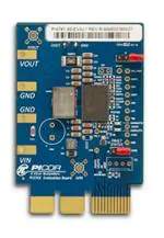
PI3741-0x-EVAL1
ZVS Regulators Buck-Boost Evaluation Board
Contents Page
Introduction 1
Bill of Materials
2
Typical Connections
4
Vicor PCB Edge
Connector Description
5
PAD Numbering
5
PAD Definitions
6
PCB Design Files
7
Introduction
The PI3741‑0x‑EVAL1 evaluation board demonstrates the features and benefits of the Vicor ZVS
Buck‑Boost regulator; pre-configured for either a 24 or 48V output voltage and rated for up to
150W. Please refer to the corresponding PI3741‑0x‑LGIZ data sheet for all power specifications. The
PI3741‑0x‑EVAL1 evaluation board is used with the following ZVS buck-boost products:
PI3741‑00‑LGIZ, PI3741‑01‑LGIZ.
The evaluation board provides several options for applying input power (VIN and GND) and output load
(VOUT and GND). The user can solder tab‑style banana jacks or wire, use threaded connectors with
retaining nuts or solder turret pins for clip-on connections.
The evaluation board comes with all of the PI3741-0x-LGIZ’s features accessible to the user. The
current‑monitor function (IMON) is set up to monitor the PI3741-0x-LGIZ's output current, sensed across
a 5mΩ resistor. The general purpose amplifier (VDIFF) comes pre-set with a gain of 2, but can be easily
reconfigured for differential measurements by adding extra 0603 resistors.
The I/O pins are brought out to the right edge of the evaluation board to allow for easy monitoring
or for adding additional circuitry. The status of the PGD pin is indicated by a dual‑colored LED; red
indicating a fault and green indicating no faults. The SYNCO (sync out) and SYNCI (sync in) pins are
accessible to allow for paralleling or for synchronizing to an external clock. Shorting J5 between IMON
and VSP on the board will connect the output of IMON to the positive input of the general purpose
amplifier, allowing for user‑designed signal scaling and conditioning.
A footprint for an external Soft-Start capacitor (0603) is available to tailor the start-up profile of the
converter. The error amplifier’s output (EAO) is brought to a pin and in conjunction with the soft-start
pin can be used for paralleling converters. The error amplifier’s input (EAIN) is not directly connected to
a pin, but connects to the pin EXT_VREF via a 10kΩ series resistor. Applying a DC voltage to this pin will
allow the user to change the regulated output voltage without changing the feedback network.
The board is designed with an edge connector to facilitate testing at the factory, but this connection
can also be used for board evaluation. The PCB is 4-layer FR-4 170Tg material with 2oz copper per layer,
ENIG pad finish and a board thickness of 0.062in.
UG:305
Page 1
�Bill of Materials
Table 1
Bill of materials
populated components
Qty
Reference
Designator
Value
Description
Manufacturer
Manufacturer
Part Number
14
C1, C2, C3, C4, C5,
C7, C8, C9, C10, C11,
C12, C13, C14, CIN1
2.2µF
Ceramic Cap, X7S,
100V, 1206
TDK
C3216X7S2A225K160AB
1
CCOMP
4.7nF
Murata
GRM188R71H472KA01D
1
D1
Fault Status
Rohm
SML-P24MUWT86
2
FT1, FT2
TEST 1, TEST 2
2
J5, J6
1
L1
1
LMAG
1
PCB
1
PI3741
ZVS Buck-Boost
1
R5
1.00kΩ
5
RDIFF1, RDIFF2,
REA3, RPGD, RSYNCI
10.0kΩ
1
REA1
Ceramic Cap, X7R,
50V, 0603
1 x 1mm Dual Color
SM LED
SM Testpoint
Keystone
5015
0.1in Header Jumper
Samtec
TSW-148-07-F-S
65nH
FP0404 Series
Inductor
Eaton
FP0404R1-R065-R
0.9µH
HCV1206 Inductor
Eaton
HCV1206-R90-R
PI37xx-xx
Edge Connector
Eval Board
VICOR
PCB0175rD
VICOR
PI3741-0x-LGIZ
Rohm
MCR03EZPFX1001
Resistor, 1%,
0.1W, 0603
Rohm
MCR03EZPFX1002
14.0kΩ for
PI3741-00
Resistor, 1%,
0.1W, 0603
Yageo
RC0603FR-0714KL
29.1kΩ for
PI3741-01
Resistor, 1%,
0.1W, 0603
KOA Speer
RN73H1JTTD2912F50
Yageo
RC0603FR-071K07L
Rohm
MCR03ERTF49R9
Rohm
MCR18EZHFLR510
Panasonic
ERJ-M1WSF5M0U
Rohm
MCR03EZPJ000
Fairchild
NC7WZ14EP6X
Rohm
MCH185CN104KK
1
REA4
1.07kΩ
1
RGP
49.9Ω
1
RIN
0.51Ω
1
RSENSE
0.005Ω
3
RSDA, RSCL, RZ1
0Ω
1
U1
NC7WZ14EP6X
1
CVDR
0.1µF
Low Voltage ZVS
B-B SIP 10 x 14mm
Resistor, 1%,
0.1W, 0603
Resistor, 1%,
0.1W, 0603
Resistor, 1%,
0.1W, 0603
Resistor, 1%,
0.25W, 1206
Resistor, 1%,
1W, 2512
Resistor, 1%,
0.1W, 0603
Dual Schmidt
trigger Inverter
Capacitor, X7R
Ceramic, 0.1µF,
50V, 0603
Non-Populated Components
Table 2
Non-populated components
Qty
Reference Designator
3
REA2, RIMON, RZ2
4
R1, R2, R3, R4
14
EAO, EXT_VREF, PGD, IMON,
SGND1, SGND2, SS/TRK, SYNCI, SYNCO,
VDIFF, VDR, VIN, VSN, VSP
3
CEAIN1, CEAO, CTRK
1
CIN2
Description
Resistor, 1%, 0.1W, 0603
Factory Use Only
Thru-hole test points, Vector K24C
Ceramic Cap, 50V, 0603
Bi-Polar Capacitor, Nichicon UPW2A330MPD or equivalent
2
JVIN, JVOUT
3
ENABLE, FT3, FT4
Johnson Jack, Tektronix 131503100
1
JGP
0.1in Header Jumper
1
C6
Capacitor, Ceramic, 1206
1
H1
Factory Test Header
SM Test point, Keystone 5015
UG:305
Page 2
�PGD
3
1
PCBNumber
PCB0203
J4
J1
A2
A1
PGND
CIN2
DNP
VIN
R3
DNP
R1
DNP
VDR
Y2
Y1
4
6
R5
D1B
PCBNumber
U1
NC7WZ14
ADDR0
PG SENSE
CIN1
VDR
1
1
5
VCC
GND
2
R4
DNP
ADDR1
R2
DNP
VDR
RSDA
PGD
ADDR1
ADDR0
VDR
3
4
1
TOP VIEW
2
RPGD
TRK
K7
PGND
G1
VIN
H1
VIN
J1
VIN
K1
VIN
K2
VIN
F2
Fiducials
F1
RSYNCI
CVDR
VDR
PGD
TRK
A1
ADDR1
A2
ADDR0
D1
E1
A3
SCL
A4
SDA
A5
EN
C6
VIN_FILT
SCL
SDA
ENABLE
C5
B1
SYNCI
C1
SYNCO
RSCL
C4
SYNCI
SYNCO
C3
DUAL LED ORIENTATION
PGD
ADDR1/FT1
ADDRO/FT2
D1A
C2
4
SCL
3
SDA
2
EN
1
SGND
SYNCI
SYNCO
C1
H1
Factory Test Header
FP0404R1
L1
VIN_F
RZ1
CCOMP
CTRK
LMAG
MECH PIN
PI3741
HCV1206-R
2
3
1
DNP
RZ2
CEAO
EAO
RIN
1
4
VSUPPLY
2
3
K4
VS1
K5
VS1
SGND
B14
TRK
A6
COMP
A8
UG:305
A13
VSN
VSP
A10
EAO
VSP
VSP
VDIFF
A11
A9
VSN
VDIFF
EAO
EAIN
A12
EAIN
ISP
ISN
IMON
K8
E14
IS+
D14
ISA14
IMON
PGND
G14
VOUT
H14
VOUT
J14
VOUT
K13
VOUT
K14
VOUT
LGH
A7
VS1
K10
VS2
K11
VS2
VS2
C7
C9
RDIFF2
RDIFF1
RIMON
DNP
C8
VSN
C13
IMON
ENABLE
DAC
DNP
CEAIN1
C12
VSP
J5
J6
RGP
C14
Tie
RSENSE
SGND
SGND
EXT_VREF
JGP
Tie
ADDR1
ENABLE
SDA
SCL
VOUT
Jumper J5 to connect IMON to VP for ATE Tes�ng.
REA3
DNP
VDIFF
REA4
REA1
REA2
C11
IMON
C10
JVOUT
13
14
15
16
17
18
19
20
21
22
23
24
P2
P4
SGND2
DNP
SGND1
DNP
1
1
J3
J2
DAC
EAO
VDIFF
VSN
VSP
SYNCO
SYNCI
PGD
ADDR0
VDR
ISN
VIN_FILT
VIN
-VO SENSE 1
-VO SENSE
+VO SENSE
+ VO SENSE 1
SAMTEC LPHS HORZ Edge Conn
1
2
3
4
5
6
7
8
9
10
11
12
P1
CN1
P3
VOUT
SAMTEC LPHS-04-24
JVIN
Figure 1
Evaluation board schematic
COMP
Page 3
Tie
�Figure 2
Evaluation board details
Typical Connections
Figure 4 illustrates the typical input supply and output load connections required to power the PI3741-x0
evaluation board. The test points on the right side of the board provide access to key nodes used to
assess the board's performance. The jumper "JGP" provides an access point that allows the user to add
a small signal in the feedback loop to make Gain/Phase measurements. The jumper J5 will connect the
IMON output signal to the positive input of the general purpose amplifier, allowing this signal to be
scaled. The J6 jumper will disable the converter when connected.
JVIN is an unpopulated "Johnson Jack" location that may be used to measure input ripple voltage.
Figure 3
Typical input and
output connections
UG:305
Page 4
�Vicor PCB Edge Connector Description
SAMTEC Reference Mechanical Drawings: based on EXTreme LPHPower™ Socket Assembly series,
available from Samtec’s website PCB Dimensions:
nn
Recommended PCB layout for LPHS-XX-XX-X-VXX-XX PCB Layout.pdf
nn
Right-angle Socket: LPHS-XX-XX-X-RTX-XX-MKT.pdf
nn
Vertical Socket: LPHS-XX-XX-X-VXX-XX-MKT.pdf
Figure 4
Edge connector details
PAD Numbering
Figure 5
Top (component) view
Figure 6
Bottom view
UG:305
Page 5
�Schematic Symbol
Figure 7
Schematic of edge connector
PAD Definitions
Table 3
PAD Definitions
PAD
Name
Descirption
P1,P2
PGND
Power ground connection for the input supply and output load
P3
VOUT
Output voltage connection
P4
VIN
1, 2, 6, 7, 8, 10
SGND
Signal ground used as reference for I/O measurements
11, 12
PGND
Power ground used as reference for input and output voltage measurements
3
ENABLE
4
SDA
Factory use only
5
SCL
Factory use only
Input voltage connection
Enable
9
ADR1
Factory use only
13
DAC
External voltage node to adjust regulated output voltage (EXT_VREF)
14
EAO
Error amplifier output
15
VDIFF
Differential amplifier output
16
VSN
Differential amplifier inverting input
17
VPN
Differential amplifier non-inverting input
18
SYNCO
Sync output pin
19
SYNCI
Sync input pin
20
PGD
Power good status pin
21
ADR0
Factory use only
22
VDR
Internal generated 5.1V supply for gate drivers and internal logic
23
ISN
Remote-sensed output voltage, after the IMON resistor
24
VIN
Input supply voltage measured at SiP’s input
UG:305
Page 6
�PCB Design Files
ODB++ evaluation board design files are available for download on the Vicor website.
Table 4
Design files
Product
Deisgn
File Format
PI3741-0x-EVAL1
ODB++
Link to Download
PI3741-0x Eval ODB++.zip
UG:305
Page 7
�Limitation of Warranties
Information in this document is believed to be accurate and reliable. HOWEVER, THIS INFORMATION
IS PROVIDED “AS IS” AND WITHOUT ANY WARRANTIES, EXPRESSED OR IMPLIED, AS TO THE
ACCURACY OR COMPLETENESS OF SUCH INFORMATION. VICOR SHALL HAVE NO LIABILITY FOR THE
CONSEQUENCES OF USE OF SUCH INFORMATION. IN NO EVENT SHALL VICOR BE LIABLE FOR ANY
INDIRECT, INCIDENTAL, PUNITIVE, SPECIAL OR CONSEQUENTIAL DAMAGES (INCLUDING, WITHOUT
LIMITATION, LOST PROFITS OR SAVINGS, BUSINESS INTERRUPTION, COSTS RELATED TO THE REMOVAL
OR REPLACEMENT OF ANY PRODUCTS OR REWORK CHARGES).
Vicor reserves the right to make changes to information published in this document, at any time
and without notice. You should verify that this document and information is current. This document
supersedes and replaces all prior versions of this publication.
All guidance and content herein are for illustrative purposes only. Vicor makes no representation or
warranty that the products and/or services described herein will be suitable for the specified use without
further testing or modification. You are responsible for the design and operation of your applications
and products using Vicor products, and Vicor accepts no liability for any assistance with applications or
customer product design. It is your sole responsibility to determine whether the Vicor product is suitable
and fit for your applications and products, and to implement adequate design, testing and operating
safeguards for your planned application(s) and use(s).
VICOR PRODUCTS ARE NOT DESIGNED, AUTHORIZED OR WARRANTED FOR USE IN LIFE SUPPORT,
LIFE-CRITICAL OR SAFETY-CRITICAL SYSTEMS OR EQUIPMENT. VICOR PRODUCTS ARE NOT CERTIFIED
TO MEET ISO 13485 FOR USE IN MEDICAL EQUIPMENT NOR ISO/TS16949 FOR USE IN AUTOMOTIVE
APPLICATIONS OR OTHER SIMILAR MEDICAL AND AUTOMOTIVE STANDARDS. VICOR DISCLAIMS
ANY AND ALL LIABILITY FOR INCLUSION AND/OR USE OF VICOR PRODUCTS IN SUCH EQUIPMENT OR
APPLICATIONS AND THEREFORE SUCH INCLUSION AND/OR USE IS AT YOUR OWN RISK.
Terms of Sale
The purchase and sale of Vicor products is subject to the Vicor Corporation Terms and Conditions of Sale
which are available at: (http://www.vicorpower.com/termsconditionswarranty)
Export Control
This document as well as the item(s) described herein may be subject to export control regulations.
Export may require a prior authorization from U.S. export authorities.
Contact Us: http://www.vicorpower.com/contact-us
Vicor Corporation
25 Frontage Road
Andover, MA, USA 01810
Tel: 800-735-6200
Fax: 978-475-6715
www.vicorpower.com
email
Customer Service: custserv@vicorpower.com
Technical Support: apps@vicorpower.com
©2018 Vicor Corporation. All rights reserved. The Vicor name is a registered trademark of Vicor Corporation.
I2C™ is a trademark of NXP Semiconductor.
EXTreme LPHPower™ is a trademark of Samtec, Inc.
All other trademarks, product names, logos and brands are property of their respective owners.
09/19
Rev 1.2
Page 8
�