ZVS Regulators
PI3741-0x
21V to 60VIN, 150W ZVS Buck-Boost Regulator
Product Description
Features & Benefits
The PI3741-0x series is a high efficiency, wide range DC-DC ZVS
Buck-Boost Regulator with two output range configurations
that utilize the same high-density System-in-Package (SiP).
Integrating controller, power switches, support components
and a high‑performance Zero-Voltage Switching (ZVS) topology
within the PI3741-0x increases point-of-load performance while
providing best-in-class power efficiency.
• Up to 97% efficiency
The PI3741-0x requires an external inductor, resistive divider and
minimal capacitors to form a complete DC-DC switching mode
buck-boost regulator.
• External frequency synchronization / interleaving
• 150W of continuous output power
(for specific conditions)
• Fast transient response
• Parallel capable with single-wire current sharing
• High-Side Current Sense Amplifier
• General Purpose Amplifier
Device
Output Voltage
Set
Range
PI3741-00-LGIZ
24V
21 – 36V
PI3741-01-LGIZ
48V
36 – 54V
• Input Over/Undervoltage Lockout (OVLO/UVLO)
• Output Overvoltage Protection (OVP)
• Overtemperature Protection (OTP)
• Fast and slow current limits
The ZVS architecture also enables high-frequency operation while
minimizing switching losses and maximizing efficiency. The high
switching frequency operation reduces the size of the external
filtering components, improves power density, and enables fast
dynamic response to line and load transients.
• –40 to 115°C operating range (TJ)
• Excellent light-load efficiency
Applications
• Telecom, Networking, Lighting
• Computing, Communications, Industrial
• Renewable Energy Systems
Package Information
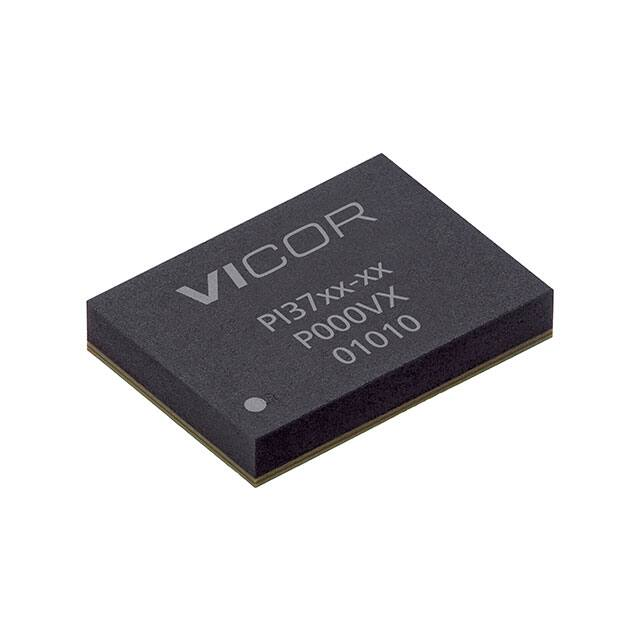
• 10 x 14 x 2.56mm LGA SiP
Typical Application
L1
VIN
VIN
CIN
VS1
VS2
VOUT
PGND
PGND
VOUT
COUT
ISP
VDR
10kΩ
PGD
ISN
PI3741
IMON
VSN
R1
VSP
EN
VDIFF
SYNCO
EAIN
EAO
SYNCI
TRK
SGND
CTRK
ZVS Regulators
Page 1 of 39
CCOMP
4700pF
Rev 2.0
08/2020
R2
COMP
�PI3741-0x
6.0
150
5.5
140
Rated Power (W)
Rated Current (A)
Rated Output Current / Power
5.0
4.5
4.0
130
120
110
100
3.5
3.0
90
20
25
30
35
40
45
50
55
80
60
20
25
30
24VOUT
32VOUT
28VOUT
36VOUT
Output Current of PI3741-00-LGIZ
21VOUT
45
50
55
60
24VOUT
32VOUT
28VOUT
36VOUT
Output Power of PI3741-00-LGIZ
4.5
160
4.0
150
Rated Power (W)
Rated Current (A)
40
Input Voltage (V)
Input Voltage (V)
21VOUT
35
3.5
3.0
2.5
2.0
140
130
120
110
100
1.5
90
20
25
30
35
40
45
50
55
60
20
Input Voltage (V)
36VOUT
40VOUT
Output Current of PI3741-01-LGIZ
ZVS Regulators
Page 2 of 39
48VOUT
25
30
35
40
45
50
55
Input Voltage (V)
54VOUT
36VOUT / 40VOUT
Output Power of PI3741-01-LGIZ
Rev 2.0
08/2020
48VOUT / 54VOUT
60
�PI3741-0x
Contents
Order Information
4
Absolute Maximum Ratings
4
Output Voltage Trim
23
Pin Description
5
Soft-Start Adjustment and Tracking
23
Package Pin-Out
6
Inductor Pairing
23
Large Pin Blocks
6
Filter Considerations
24
Storage and Handling Information
7
Thermal Design
26
Block Diagram
7
PI3741-00-LGIZ Percentage of SiP Loss to Total Loss
30
PI3741-00-LGIZ Electrical Characteristics
8
PI3741-01-LGIZ Percentage of SiP Loss to Total Loss
31
PI3741-01-LGIZ Electrical Characteristics
11
Evaluation Board Thermal De-rating
32
PI3741-00-LGIZ Performance Characteristics TA = 25°C
14
Parallel Operation
34
PI3741-01-LGIZ Performance Characteristics TA = 25°C
17
Synchronization 34
MTBF 20
Interleaving 34
Functional Description
VDR Bias Regulator
35
System Design Considerations
35
21
Enable 21
Application Description
23
Switching Frequency Synchronization
21
Inductive Loads
35
Soft-Start and Tracking
21
Low Voltage Operation
35
Remote Sensing Differential Amplifier
21
Package Drawings
36
Power Good
21
Receiving PCB Pattern Design Recommendations
37
Output Current Limit Protection
21
Revision History
38
Input Undervoltage Lockout
21
Warranty 39
Input Overvoltage Lockout
21
Output Overvoltage Protection
22
Overtemperature Protection
22
Pulse Skip Mode (PSM)
22
Variable Frequency Operation
22
IMON Amplifier
22
ZVS Regulators
Page 3 of 39
Rev 2.0
08/2020
�PI3741-0x
Order Information
Part Number
Description
Package
Transport Media
MFG
PI3741-00-LGIZ
21 – 60VIN to 21 – 36VOUT
10mm x 14mm 108-pin LGA
TRAY
Vicor
PI3741-01-LGIZ
21 – 60VIN to 36 – 54VOUT
10mm x 14mm 108-pin LGA
TRAY
Vicor
Absolute Maximum Ratings
Note: Stresses beyond these limits may cause permanent damage to the device. Operation at these conditions or conditions beyond those listed in the
Electrical Specifications table is not guaranteed. All voltage nodes are referenced to PGND unless otherwise noted.
Location
VMIN
ISOURCE
[1]
40A [1]
75V
–0.7V
4–5, G–K
VS1
75V
–0.7VDC
40A [1]
18A [1]
10–11, G–K
VS2
75V
–0.7VDC
40A [1]
18A [1]
13–14, G–K
VOUT
75V
–0.7VDC
40A [1]
40A [1]
1E
VDR
5.5V
–0.3V
30mA
200mA
1D
PGD
5.5V
–0.3V
20mA
20mA
1C
SYNCO
5.5V
–0.3V
5mA
5mA
1B
SYNCI
5.5V
–0.3V
5mA
5mA
1A
FT1
5.5V
–0.3V
5mA
5mA
2A
FT2
5.5V
–0.3V
5mA
5mA
3A
FT3
5.5V
–0.3V
5mA
5mA
4A
FT4
5.5V
–0.3V
10mA
10mA
5A
EN
5.5V
–0.3V
5mA
5mA
6A
TRK
5.5V
–0.3V
50mA
50mA
7A
LGH
5.5V
–0.3V
5mA
5mA
8A
COMP
5.5V
–0.3V
5mA
5mA
9A
VSN
5.5V
–1.5V
5mA
5mA
10A
VSP
5.5V
–1.5V
5mA
5mA
11A
VDIFF
5.5V
–0.5V
5mA
5mA
12A
EAIN
5.5V
–0.3V
5mA
5mA
13A
EAO
5.5V
–0.3V
5mA
5mA
14A
IMON
5.5V
–0.3V
5mA
5mA
14D
ISN
[2]
75V
–2VDC
5mA
5mA
ISP
[2]
75V
–2VDC
5mA
5mA
SGND
0.3V
–0.3V
200mA
200mA
[1]
18A [1]
2–9, B–E + 7–8, F–K
PGND
N/A
N/A
Non-Operating Test Mode Limits.
The ISP pin to ISN pin has a maximum differential limit of +5.5VDC and -0.5VDC.
ZVS Regulators
Page 4 of 39
Rev 2.0
08/2020
40A
ISINK
VIN
10–14, B + 10–12, C–E
[2]
VMAX
1–2, G–K
14E
[1]
Name
18A
�PI3741-0x
Pin Description
Pin Number
Pin Name
1–2, G–K
VIN
Input voltage and sense node for UVLO, OVLO and feed forward compensation.
4–5, G–K
VS1
Input side switching node and ZVS sense node for power switches.
10–11, G–K
VS2
Output side switching node and ZVS sense node for power switches.
13–14, G–K
VOUT
1E
VDR
Internal 5.1V supply for gate drivers and internal logic. May be used as reference or low power bias supply
for up to 2mA. Must be impedance limited by the user.
1D
PGD
Fault & Power Good indicator. PGD pulls low when the regulator is not operating or if EAIN is less
than 1.4V.
1C
SYNCO
Synchronization output. Outputs a high signal for ½ of the programmed switching period at the beginning
of each switching cycle, for synchronization of other regulators.
1B
SYNCI
Synchronization input. When a falling edge synchronization pulse is detected, the PI3741-0x will delay
the start of the next switching cycle until the next falling edge sync pulse arrives, up to a maximum delay
of two times the programmed switching period. If the next pulse does not arrive within two times the
programmed switching period, the controller will leave sync mode and start a switching cycle automatically.
Connect to SGND when not in use.
1A
FT1
For factory use only. Connect to SGND or leave floating in application.
2A
FT2
For factory use only. Connect to SGND or leave floating in application.
3A
FT3
For factory use only. Connect to SGND in application.
4A
FT4
For factory use only. Connect to SGND in application.
5A
EN
Regulator Enable control. Asserted high or left floating – regulator enabled;
Asserted low, regulator output disabled.
6A
TRK
Soft-start and track input. An external capacitor may be connected between TRK pin and SGND to decrease
the rate of output rise during soft-start.
7A
LGH
For factory use only. Connect to SGND in application.
8A
COMP
9A
VSN
General purpose amplifier inverting input.
10A
VSP
General purpose amplifier non-inverting input.
11A
VDIFF
General Purpose amplifier output. When unused connect VDIFF to VSN and VSP to SGND.
12A
EAIN
Error amplifier inverting input and sense for PGD. Connect by resistive divider to the output.
13A
EAO
Error amp output: External connection for additional compensation and current sharing. Leave floating
to use the internal error amplifier capacitance for default loop compensation. Please contact Applications
Support if additional compensation is needed.
14A
IMON
14D
ISN
High side current sense amplifier negative input.
14E
ISP
High side current sense amplifier positive input.
10–14, B + 10–12, C–E
SGND
Signal ground. Internal logic and analog ground for the regulator. SGND and PGND are star connected
within the regulator package.
2–9, B-E + 7–8, F–K
PGND
Power ground. VIN, VOUT, VS1 and VS2 power returns. SGND and PGND are star connected within the
regulator package.
ZVS Regulators
Page 5 of 39
Description
Output voltage and sense node for power switches, VOUT feed forward compensation, VOUT_OV
and internal signals.
Error amp compensation dominant pole. Connect a capacitor of 4700pF by default between COMP
and SGND to set the control loop dominant pole. If the application requires output capacitance from
recommended in table 1, please contact Applications Support to compensate the control loop.
High side current sense amplifier output.
Rev 2.0
08/2020
�PI3741-0x
Package Pin-Out
1
FT1
SYNCI
SYNC0
PGD/
FLT
VDR
VIN
VIN
VIN
VIN
2
FT2
PGND
PGND
PGND
PGND
VIN
VIN
VIN
VIN
3
FT3
PGND
PGND
PGND
PGND
4
FT4
PGND
PGND
PGND
PGND
VS1
VS1
VS1
VS1
5
EN
PGND
PGND
PGND
PGND
VS1
VS1
VS1
VS1
6
TRK
PGND
PGND
PGND
PGND
7
LGH/
FT5
PGND
PGND
PGND
PGND
PGND
PGND
PGND
PGND
PGND
8
COMP
PGND
PGND
PGND
PGND
PGND
PGND
PGND
PGND
PGND
9
VSN
PGND
PGND
PGND
PGND
10
VSP
SGND
SGND
SGND
SGND
VS2
VS2
VS2
VS2
11
VDIFF
SGND
SGND
SGND
SGND
VS2
VS2
VS2
VS2
12
EAIN
SGND
SGND
SGND
SGND
13
EAO
SGND
VOUT
VOUT
VOUT
VOUT
14
IMON
SGND
VOUT
VOUT
VOUT
VOUT
ISN
ISP
Large Pin Blocks
Pin Block Name
Group of pins
VIN
G1-2, H1-2, J1-2, K1-2
VS1
G4-5, H4-5, J4-5, K4-5
PGND
B2-9, C2-9, D2-9, E2-9, F7-8, G7-8, H7-8, J7-8, K7-8
VS2
G10-11, H10-11, J10-11, K10-11
VOUT
G13-14, H13-14, J13-14, K13-14
SGND
B10-14, C10-12, D10-12, E10-12
ZVS Regulators
Page 6 of 39
Rev 2.0
08/2020
�PI3741-0x
Storage and Handling Information
Maximum Storage Temperature Range
-65°C to 150°C
Maximum Operating Junction Temperature Range
-40°C to 115°C
Soldering Temperature for 20 seconds
245°C
MSL Rating
3
ESD Rating
[3]
[3]
2.0kV HBM; 1.0kV CDM
JS-200-2014, JESD22-A114F.
Block Diagram
VS1 VS2
VIN
VOUT
Q1
Q3
VS1
VS2
Q2
Q4
+
+
LDO
VDR
SYNCO
SYNCI
PGD
EN
FT1 - FT5
ZVS Buck Boost Control
and
Digital Parametric Trim
+ VREF
0Ω
F1
Rev 2.0
08/2020
F2
F3
F4
SGND
ZVS Regulators
Page 7 of 39
ISP
IMON
VSN
VSP
VDIFF
EAIN
EAO
COMP
CLAMP
PGND
ISN
TRK
�PI3741-0x
PI3741-00-LGIZ Electrical Characteristics
Specifications apply for the conditions -40°C < TJ < 115°C, VIN = 48V, VOUT = 24V, LEXT = 900nH [4], external CIN = 5 x 2.2µF, external COUT = 8 x 2.2µF,
unless otherwise noted.
Parameter
Symbol
Conditions
Min
Typ
Max
Unit
21
48
60
V
Input Specifications
Input Voltage
Input Current During Output Short
(Fault Condition Duty Cycle)
VIN_DC
IIN_SHORT
[5]
Input Quiescent Current
IQ_VIN
Enabled (no load)
Input Quiescent Current
IQ_VIN
Disabled
VIN_SR
[5]
Input Voltage Slew Rate
1.9
mA
4
mA
1.5
mA
1
Internal Input Capacitance
CIN
0.5
µF
VIN UVLO Threshold Rising
VIN_UVLO_START
19.2
V
VIN_UVLO_HYS
0.7
V
VIN UVLO Hysteresis
VIN OVLO Threshold Rising
VIN OVLO Hysteresis
25°C, VIN = 48V
V / µs
VIN_OVLO_START
61
VIN_OVLO_HYS
64.5
68
1.3
V
V
Output Specifications
EAIN Voltage Total Regulation
VEAIN_DC
Output Voltage Range
VOUT_DC
Output Current Range
IOUT_DCR
Output Current Steady State
IOUT_DC
Output Power Steady State
POUT_DC
[6]
1.667
1.7
1.734
V
21
24
36
V
max
A
0
VIN = 21 – 48V, VOUT ≤ 24V, TCASE = 25°C [6]
4.17
VIN = 48 – 60V, VOUT ≤ 24V, TCASE = 25°C [6]
5.42
VIN = 21 – 48V, VOUT = 24 – 36V, TCASE = 25°C [6]
100
[6]
130
VIN = 48 – 60V, VOUT = 24 – 36V, TCASE = 25°C
A
W
Line Regulation
∆VOUT(∆VIN)
@ 25°C, 21V < VIN < 60V
0.10
%
Load Regulation
∆VOUT(∆IOUT)
@ 25°C, IOUT above 5% of the typical full load
0.10
%
IOUT = 5.42A, VIN = 48V, VOUT = 24V, TCASE = 25°C
COUT_EX = 8 x 2.2µF, 100V, X7R, 20MHz BW
208
mVp-p
25°C, VOUT = 24V
0.75
µF
Output Ripple
VOUT_AC
Internal Output Capacitance
COUT
VOUT Overvoltage Threshold
VOUT_OVT
VOUT Overvoltage Hysteresis
VOUT_OVH
Rising VOUT threshold to detect open loop
39.8
41.9
44
0.8
V
V
VDR
VDR Supply Voltage
VDR
Generated internally
4.9
5.1
5.36
V
150
260
µA
Current Sense Amplifier (Dedicated to monitor Input or Output Current)
ISP Pin Bias Current (Sink)
VOUT = 10V, Flows to SGND
ISN Pin Bias Current
VOUT = 10V
90
0
Common Mode Input Range
8
IMON Source Current
1
IMON Sink Current
IMON Output At No Load
µA
60
V
1.8
3
mA
1
1.6
2.6
mA
0
10
20
mV
4
%
Full Scale Error
40mV input
Bandwidth
[5]
40
1%
20
µs
20
V/V
Settling Time For Full Scale Step
Gain
ZVS Regulators
Page 8 of 39
-4
AV_CS
Rev 2.0
08/2020
kHz
�PI3741-0x
PI3741-00-LGIZ Electrical Characteristics (Cont.)
Specifications apply for the conditions -40°C < TJ < 115°C, VIN = 48V, VOUT = 24V, LEXT = 900nH [4], external CIN = 5 x 2.2µF, external COUT = 8 x 2.2µF,
unless otherwise noted.
Parameter
Symbol
Conditions
Min
Typ
Max
Unit
Open Loop Gain
[5]
96
120
140
dB
Small Signal Gain-Bandwidth
[5]
5
7
12
MHz
-1
1
mV
-0.1
2.5
V
2
V
VDR – 0.2V
V
20
mV
100
pF
General Purpose Amplifier
Offset
Common Mode Input Range
Differential Mode Input Range
Maximum Output Voltage
IDIFF = -1mA
Minimum Output Voltage
No Load
Capacitive Load for Stable
Operation
[5]
0
Slew Rate
10
Output Current
-1
V / µs
1
mA
Transconductance Error Amplifier
Reference
VREF
Input Range
VEAIN
EAIN = EAO, 25ºC
1.688
1.7
1.712
EAIN = EAO
1.674
1.7
1.726
Note VEAIN_OV below
0
Maximum Output Voltage
3.35
Minimum Output Voltage
V
VDR
V
3.6
4.0
V
0.05
0.15
V
Transconductance
Factory Set
7.6
mS
Zero Resistor
Factory Set
6
kΩ
EAO Output Current Sourcing
VEAO = 50mV, VEAIN = 0V
400
µA
EAO Output Current Sinking
VEAO = 2V, VEAIN = 5V
400
µA
80
dB
Input Capacitance
56
pF
Output Capacitance
56
pF
1
MHz
0.4
V
Open Loop Gain
ROUT > 1MΩ
[5]
70
Control and Protection
Switching Frequency
VEAO Pulse Skip Threshold
Control Node Range
VEAO Overload Threshold
Overload Timeout
Overload due to EAO limit
VEAIN Output Overvoltage Threshold
Overtemperature Fault Threshold
Overtemperature Restart Hysteresis
FSW
VEAO_PST
VEAO to SGND
VRAMP
0
VEAO_OL
VEAO to SGND
TOL
VEAO > VEAO_OL
IOUT_EAOLIM
VEAIN_OV
3.175
Module shuts down after 1ms of overload and restarts
after 30ms
VEAIN > VEAIN_OV
1.94
3.3
V
3.425
V
1
ms
6.8
A
2.04
2.14
V
TOTP
[5]
125
°C
TOPT_HYS
[5]
30
°C
VOUT Negative Fault Threshold
ZVS Regulators
Page 9 of 39
3.3
-0.45
Rev 2.0
08/2020
-0.25
-0.15
V
�PI3741-0x
PI3741-00-LGIZ Electrical Characteristics (Cont.)
Specifications apply for the conditions -40°C < TJ < 115°C, VIN = 48V, VOUT = 24V, LEXT = 900nH [4], external CIN = 5 x 2.2µF, external COUT = 8 x 2.2µF,
unless otherwise noted.
Parameter
Symbol
Conditions
Min
Typ
Max
Unit
1.7
V
70
mV
Soft Start and Tracking Function
TRK Active Range
Nominal
0
TRK Disable Threshold
20
TRK Internal Capacitance
Soft Start Charge Current
30
Soft Start Discharge Current
Soft Start Time
45
.047
VTRK = 0.5V
tSS
Ext CSS = 0μF
50
µF
70
µA
9
mA
1.6
ms
Enable
Enable High Threshold
ENIH
0.9
1
1.1
V
Enable Low Threshold
ENIL
0.7
0.8
0.9
V
200
300
mV
Enable Threshold Hysteresis
ENHYS
100
Enable Pin Bias Current
VEN = 0V or VEN = 2V
±50
µA
Enable Pull-up Voltage
Floating
2.0
V
30
ms
Fault Restart Delay Time
tFR_DLY
Digital Signals
SYNCI High Threshold
VDR = 5.1V
SYNCO High
SYNCOOH
SYNCO Low
SYNCOOL
1/2 VDR
VDR - 0.5
ISYNCO = 1mA
V
VDR
V
0.5
V
PGD High Leakage
PGDILH
VPGD = VDR
10
µA
PGD Output Low
PGDOL
IPGD = 4mA
0.4
V
PGD EAIN Low Rise
1.41
1.45
1.48
V
PGD EAIN Low Fall
1.36
1.41
1.46
V
1.94
2.04
PGD EAIN Threshold Hysteresis
PGD EAIN High
[4]
35
See Inductor Pairing section.
Assured to meet performance specification by design, test correlation, characterization, and / or statistical process control.
[6] Output current capability varies with input & output voltage. See rated output current / power curves on page 2.
[5]
ZVS Regulators
Rev 2.0
Page 10 of 39 08/2020
mV
2.14
V
�PI3741-0x
PI3741-01-LGIZ Electrical Characteristics
Specifications apply for the conditions -40°C < TJ < 115°C, VIN = 48V, VOUT = 48V, LEXT = 900nH [4], external CIN = 5 x 2.2µF, external COUT = 8 x 2.2µF,
unless otherwise noted.
Parameter
Symbol
Conditions
Min
Typ
Max
Unit
21
48
60
V
Input Specifications
Input Voltage
Input Current During Output Short
(Fault Condition Duty Cycle)
VIN_DC
IIN_SHORT
[5]
Input Quiescent Current
IQ_VIN
Enabled (no load)
Input Quiescent Current
IQ_VIN
Disabled
VIN_SR
[5]
Input Voltage Slew Rate
1.9
mA
5
mA
1.5
mA
1
Internal Input Capacitance
CIN
0.5
µF
VIN UVLO Threshold Rising
VIN_UVLO_START
19.2
V
VIN_UVLO_HYS
0.7
V
VIN UVLO Hysteresis
VIN OVLO Threshold Rising
VIN OVLO Hysteresis
25°C, VIN = 48V
V / µs
VIN_OVLO_START
61
VIN_OVLO_HYS
64.5
68
1.3
V
V
Output Specifications
EAIN Voltage Total Regulation
VEAIN_DC
Output Voltage Range
VOUT_DC
Output Current Range
IOUT_DCR
Output Current Steady State
IOUT_DC
Output Power Steady State
POUT_DC
[6]
1.667
1.7
1.734
V
36
48
54
V
max
A
0
VIN = 21 – 48V, VOUT ≤ 48V, TCASE = 25°C [6]
2.09
VIN = 48 – 60V, VOUT ≤ 48V, TCASE = 25°C [6]
3.13
VIN = 21 – 48V, VOUT = 48 – 54V, TCASE = 25°C [6]
100
[6]
150
VIN = 48 – 60V, VOUT = 48 – 54V, TCASE = 25°C
A
W
Line Regulation
∆VOUT(∆VIN)
@ 25°C, 21V < VIN < 60V
0.10
%
Load Regulation
∆VOUT(∆IOUT)
@ 25°C, IOUT above 5% of the typical full load
0.10
%
IOUT = 3.13A, VIN = 48V, VOUT = 48V, TCASE = 25°C
COUT_EX = 8 x 2.2µF, 100V, X7R, 20MHz BW
320
mVp-p
25°C, VOUT = 48V
0.5
µF
Output Ripple
VOUT_AC
Internal Output Capacitance
COUT
VOUT Overvoltage Threshold
VOUT_OVT
VOUT Overvoltage Hysteresis
VOUT_OVH
Rising VOUT threshold to detect open loop
60
63.1
66.3
1.3
V
V
VDR
VDR Supply Voltage
VDR
Generated Internally
4.9
5.1
5.36
V
150
260
µA
Current Sense Amplifier (Dedicated to monitor Input or Output Current)
ISP Pin Bias Current (Sink)
VOUT = 10V, Flows to SGND
ISN Pin Bias Current
VOUT = 10V
90
0
Common Mode Input Range
8
IMON Source Current
1
IMON Sink Current
1
IMON Output At No Load
0
-4
µA
60
V
1.8
3
mA
1.6
2.6
mA
10
mV
4
%
Full Scale Error
40mV input
Bandwidth
[5]
40
1%
20
µs
20
V/V
Settling Time For Full Scale Step
Gain
AV_CS
ZVS Regulators
Rev 2.0
Page 11 of 39 08/2020
kHz
�PI3741-0x
PI3741-01-LGIZ Electrical Characteristics (Cont.)
Specifications apply for the conditions -40°C < TJ < 115°C, VIN = 48V, VOUT = 48V, LEXT = 900nH [4], external CIN = 5 x 2.2µF, external COUT = 8 x 2.2µF,
unless otherwise noted.
Parameter
Symbol
Conditions
Min
Typ
Max
Unit
Open Loop Gain
[5]
96
120
140
dB
Small Signal Gain-Bandwidth
[5]
5
7
12
MHz
-1
1
mV
-0.1
2.5
V
2
V
VDR – 0.2V
V
20
mV
100
pF
General Purpose Amplifier
Offset
Common Mode Input Range
Differential Mode Input Range
Maximum Output Voltage
IDIFF = -1mA
Minimum Output Voltage
No Load
Capacitive Load for Stable
Operation
[5]
0
Slew Rate
10
Output Current
-1
V / µs
1
mA
Transconductance Error Amplifier
Reference
VREF
Input Range
VEAIN
EAIN = EAO, 25ºC
1.688
1.7
1.712
EAIN = EAO
1.674
1.7
1.726
Note VEAIN_OV below
Maximum Output Voltage
0
3.35
Minimum Output Voltage
V
VDR
V
3.6
4.0
V
0.05
0.15
V
Transconductance
Factory Set
5.1
mS
Zero Resistor
Factory Set
5
kΩ
EAO Output Current Sourcing
VEAO = 50mV, VEAIN = 0V
400
µA
EAO Output Current Sinking
VEAO = 2V, VEAIN = 5V
400
µA
80
dB
Input Capacitance
56
pF
Output Capacitance
56
pF
1
MHz
0.4
V
Open Loop Gain
ROUT > 1MΩ
[5]
70
Control and Protection
Switching Frequency
VEAO Pulse Skip Threshold
Control Node Range
VEAO Overload Threshold
Overload Timeout
Overload due to EAO limit
VEAIN Output Overvoltage Threshold
Overtemperature Fault Threshold
Overtemperature Restart Hysteresis
FSW
VEAO_PST
VEAO to SGND
VRAMP
0
VEAO_OL
VEAO to SGND
TOL
VEAO > VEAO_OL
IOUT_EAOLIM
VEAIN_OV
3.175
Module shuts down after 1ms of overload and restarts
after 30ms
VEAIN > VEAIN_OV
1.94
3.3
3.3
V
3.425
V
1
ms
5.0
A
2.04
2.14
V
TOTP
[5]
125
°C
TOPT_HYS
[5]
30
°C
VOUT Negative Fault Threshold
ZVS Regulators
Rev 2.0
Page 12 of 39 08/2020
-0.45
-0.25
-0.15
V
�PI3741-0x
PI3741-01-LGIZ Electrical Characteristics (Cont.)
Specifications apply for the conditions -40°C < TJ < 115°C, VIN = 48V, VOUT = 48V, LEXT = 900nH [4], external CIN = 5 x 2.2µF, external COUT = 8 x 2.2µF,
unless otherwise noted.
Parameter
Symbol
Conditions
Min
Typ
Max
Unit
1.7
V
70
mV
Soft Start and Tracking Function
TRK Active Range
Nominal
0
TRK Disable Threshold
20
TRK Internal Capacitance
Soft Start Charge Current
30
Soft Start Discharge Current
Soft Start Time
45
.047
VTRK = 0.5V
tSS
Ext CSS = 0μF
50
µF
70
µA
9
mA
1.6
ms
Enable
Enable High Threshold
ENIH
0.9
1
1.1
V
Enable Low Threshold
ENIL
0.7
0.8
0.9
V
200
300
mV
Enable Threshold Hysteresis
ENHYS
100
Enable Pin Bias Current
VEN = 0V or VEN = 2V
±50
µA
Enable Pull-up Voltage
Floating
2.0
V
30
ms
Fault Restart Delay Time
tFR_DLY
Digital Signals
SYNCI High Threshold
VDR = 5.1V
SYNCO High
SYNCOOH
SYNCO Low
SYNCOOL
1/2 VDR
VDR - 0.5
ISYNCO = 1mA
V
VDR
V
0.5
V
PGD High Leakage
PGDILH
VPGD = VDR
10
µA
PGD Output Low
PGDOL
IPGD = 4mA
0.4
V
PGD EAIN Low Rise
1.41
1.45
1.48
V
PGD EAIN Low Fall
1.36
1.41
1.46
V
1.94
2.04
PGD EAIN Threshold Hysteresis
PGD EAIN High
[4]
35
See Inductor Pairing section.
Assured to meet performance specification by design, test correlation, characterization, and/or statistical process control.
[6] Output current capability varies with input & output voltage. See rated output current / power curves on page 2.
[5]
ZVS Regulators
Rev 2.0
Page 13 of 39 08/2020
mV
2.14
V
�PI3741-0x
PI3741-00-LGIZ Performance Characteristics TA = 25°C
98
Efficiency (%)
97
96
95
94
93
92
91
90
0
1
2
3
4
5
6
Output Current (A)
21VIN
48VIN
60VIN
Figure 1 — 24VOUT Efficiency
Figure 4 — 48VIN to 24VOUT, COUT = 8 x 2.2µF Ceramic
5.42A to 2.71A Load Step, 0.1A/µs
98
Efficiency (%)
97
96
95
94
93
92
91
90
0
1
2
3
4
5
6
Output Current (A)
21VIN
48VIN
60VIN
Figure 2 — 21VOUT Efficiency
Figure 5 — 60VIN to 21VOUT, COUT = 8 x 2.2µF Ceramic
5.72A to 2.86A Load Step, 0.1A/µs
98
Efficiency (%)
97
96
95
94
93
92
91
0
1
2
3
4
Output Current (A)
21VIN
Figure 3 — 36VOUT Efficiency
48VIN
60VIN
Figure 6 — 21VIN to 36VOUT, COUT = 8 x 2.2µF Ceramic
3.34A to 1.67A Load Step, 0.1A/µs
ZVS Regulators
Rev 2.0
Page 14 of 39 08/2020
�PI3741-0x
Operational Frequency (kHz)
PI3741-00-LGIZ Performance Characteristics TA = 25°C (Cont.)
1100
1000
900
800
700
600
500
400
300
200
100
0
0
1
2
3
4
5
6
Output Current (A)
21VIN
48VIN
60VIN
Operational Frequency (kHz)
Figure 7 — Switching Frequency vs. Output Current @ 24VOUT
Figure 10 — Start-up with 48VIN to 24VOUT at 5.42A,
Ext CSS = 0µF
1100
1000
900
800
700
600
500
400
300
200
100
0
0
1
2
3
4
5
6
Output Current (A)
21VIN
48VIN
60VIN
Operational Frequency (kHz)
Figure 8 — Switching Frequency vs. Output Current @ 21VOUT
Figure 11 — Output voltage ripple at 48VIN to 24VOUT, 5.42A;
COUT = 8 x 2.2µF Ceramic
1100
1000
900
800
700
600
500
400
300
200
100
0
0
0.5
1
1.5
2
2.5
3
3.5
4
Output Current (A)
21VIN
48VIN
60VIN
Figure 9 — Switching Frequency vs. Output Current @ 36VOUT
ZVS Regulators
Rev 2.0
Page 15 of 39 08/2020
�PI3741-0x
PI3741-00-LGIZ Efficiency & Power Loss TA = 25°C [7] (Cont.)
4.5
99
4
Efficiency (%)
97
96
3.5
95
94
3
93
92
2.5
Power Dissipation (W)
98
91
90
20
25
30
35
40
45
50
55
60
2
VIN (V)
Efficiency
Power Dissipation
Figure 12 — 24VOUT Efficiency and Power Dissipation at maximum
current (4.17A) over full input dynamic range
4.5
99
4
Efficiency (%)
97
96
3.5
95
94
3
93
92
2.5
Power Dissipation (W)
98
91
90
20
25
30
35
40
45
50
55
60
2
VIN (V)
Efficiency
Power Dissipation
Figure 13 — 21VOUT Efficiency and Power Dissipation at maximum
current (4.29A) over full input dynamic range
4.5
99
4
Efficiency (%)
97
96
3.5
95
94
3
93
92
2.5
Power Dissipation (W)
98
91
90
20
25
30
35
40
45
50
55
60
2
VIN (V)
Efficiency
Power Dissipation
Figure 14 — 36VOUT Efficiency and Power Dissipation at maximum
current (3.34A) over full input dynamic range
[7]
Note: Testing was performed using a 3in. x 3in., four 2oz. copper layers, FR4 evaluation board platform.
ZVS Regulators
Rev 2.0
Page 16 of 39 08/2020
�PI3741-0x
PI3741-01-LGIZ Performance Characteristics TA = 25°C
98
Efficiency (%)
96
94
92
90
88
86
0
1
2
3
4
Output Current (A)
21VIN
48VIN
60VIN
Figure 15 — 48VOUT Efficiency
Figure 18 — 48VIN to 48VOUT, COUT = 8 x 2.2µF Ceramic
3.13A to 1.57A Load Step, 0.1A/µs
98
97
Efficiency (%)
96
95
94
93
92
91
0
1
2
4
3
5
Output Current (A)
21VIN
48VIN
60VIN
Figure 16 — 36VOUT Efficiency
Figure 19 — 60VIN to 36VOUT, COUT = 8 x 2.2µF Ceramic
4.17A to 2.09A Load Step, 0.1A/µs
98
Efficiency (%)
96
94
92
90
88
86
84
0
1
2
3
Output Current (A)
21VIN
Figure 17 — 54VOUT Efficiency
48VIN
60VIN
Figure 20 — 21VIN to 54VOUT, COUT = 8 x 2.2µF Ceramic
1.86A to 0.93A Load Step, 0.1A/µs
ZVS Regulators
Rev 2.0
Page 17 of 39 08/2020
�PI3741-0x
Operational Frequency (kHz)
PI3741-01-LGIZ Performance Characteristics TA = 25°C (Cont.)
1100
1000
900
800
700
600
500
400
300
200
100
0
0
0.5
1
1.5
2
2.5
3
3.5
4
Output Current (A)
21VIN
48VIN
60VIN
Operational Frequency (kHz)
Figure 21 — Switching Frequency vs. Output Current @ 48VOUT
Figure 24 — Start-up with 48VIN to 48VOUT at 3.13A, Ext CSS = 0µF
1100
1000
900
800
700
600
500
400
300
200
100
0
0
0.5
1
1.5
2
2.5
3
3.5
4
4.5
5
Output Current (A)
21VIN
48VIN
60VIN
Operational Frequency (kHz)
Figure 22 — Switching Frequency vs. Output Current @ 36VOUT
Figure 25 — Output voltage ripple at 48VIN to 48VOUT,
3.13A; COUT = 8 x 2.2µF Ceramic
1100
1000
900
800
700
600
500
400
300
200
100
0
0
0.5
1
1.5
2
2.5
3
Output Current (A)
21VIN
48VIN
60VIN
Figure 23 — Switching Frequency vs. Output Current @ 54VOUT
ZVS Regulators
Rev 2.0
Page 18 of 39 08/2020
�PI3741-0x
PI3741-01-LGIZ Efficiency & Power Loss TA = 25°C [7] (Cont.)
99
4.5
Efficiency (%)
97
96
4
95
3.5
94
3
93
92
2.5
91
90
20
25
30
35
40
45
50
55
60
Power Dissipation (W)
5
98
2
VIN (V)
Efficiency
Power Dissipation
99
4
98
3.8
97
3.6
3.4
96
3.2
95
3
94
2.8
93
2.6
92
2.4
91
2.2
90
Power Dissipation (W)
Efficiency (%)
Figure 26 — 48VOUT Efficiency and Power Dissipation at maximum
current (2.09A) over full input dynamic range
2
20
25
30
35
40
45
50
55
60
VIN (V)
Efficiency
Power Dissipation
Figure 27 — 36VOUT Efficiency and Power Dissipation at maximum
current (2.78A) over full input dynamic range
5.5
98
5
Efficiency (%)
97
4.5
96
95
4
94
3.5
93
92
3
91
90
20
25
30
35
40
45
50
55
60
Power Dissipation (W)
99
2.5
VIN (V)
Efficiency
Power Dissipation
Figure 28 — 54VOUT Efficiency and Power Dissipation at maximum
current (1.86A) over full input dynamic range
[7]
Note: Testing was performed using a 3in. x 3in., four 2oz. copper layers, FR4 evaluation board platform.
ZVS Regulators
Rev 2.0
Page 19 of 39 08/2020
�PI3741-0x
MTBF
MTBF (Mhrs)
1000
100
10
1
-60
-40
-20
0
20
40
60
80
100
Temperature (°C)
MTBF Calculations Over Temperature Using Telcordia SR-332
Figure 29 — PI3741-0x calculated MTBF Telcordia SR-332 GB
ZVS Regulators
Rev 2.0
Page 20 of 39 08/2020
120
140
�PI3741-0x
Functional Description
The PI3741-0x is a family of highly integrated ZVS Buck‑Boost
regulators. The PI3741-0x has an adjustable output voltage that
is set with a resistive divider. Performance and maximum output
current are characterized with a specific external power inductor
as defined in the electrical specifications, and in the inductor
pairing section.
L1
VIN
CIN
VIN
VS1
VS2
VOUT
PGND
PGND
VOUT
COUT
ISP
VDR
10kΩ
PGD
47nF soft-start capacitor to set the start-up ramp period greater
than tSS. The PI3741-0x internal reference and regulated output
will proportionally follow the TRK ramp when it is below 1.7VDC.
When the ramp is greater than 1.7VDC, the internal reference will
remain at 1.7VDC while the TRK ramp rises and clamps at 2.5VDC.
If the TRK pin goes below the disable threshold, the regulator will
finish the current switching cycle and then stop switching.
Remote Sensing Differential Amplifier
A general purpose operational amplifier is provided to assist with
differential remote sensing and/or level shifting of the output
voltage. The VDIFF pin can be connected to the transconductance
error amplifier input EAIN pin, or with proper configuration can
also be connected to the EAO pin to drive the modulator directly.
If unused, connect in unity gain with VSP connected to SGND.
ISN
PI3741
IMON
Power Good
VSN
R1
VSP
EN
VDIFF
SYNCO
EAIN
SYNCI
TRK
EAO
SGND
R2
COMP
CCOMP
4700pF
Figure 30 — ZVS Buck-Boost with required components
For basic operation, Figure 30 shows the minimum connections
and components required.
Enable
The EN pin of the regulator is referenced to SGND and permits the
user to turn the regulator on or off. The EN polarity is a positive
logic assertion. If the EN pin is left floating or asserted high, the
regulator output is enabled. Pulling the EN pin below 0.8VDC with
respect to SGND will discharge the SS/TRK pin until the output
reaches zero or the EN pin is released. When the converter is
disabled via the EN pin or due to a fault mode, the internal gate
driver high side charge pumps are enabled as long as there is
enough input voltage for the internal VDR supply voltage to be
available. The return path for this charge pump supply is through
the output. If the output load is disconnected or high impedance,
the output capacitors will float up to about 3.4V maximum,
sourced by 960µA of leakage current. This pre-biased condition
poses no issue for the converter. The 960µA leakage current
may be safely bypassed to SGND. A simple application circuit is
available to bypass this current in a non-dissipative manner. Please
contact Applications Engineering for details.
Switching Frequency Synchronization
The SYNCI input allows the user to synchronize the controller
switching frequency to the falling edge of an external clock
referenced to SGND. The external clock can synchronize the unit
between 50% and 110% of the preset switching frequency (FSW ).
The SYNCI pin should be connected to SGND when not in use,
and should never be left floating.
Soft-Start and Tracking
The PI3741-0x provides a soft start and tracking feature using
the TRK pin. Programmable Soft Start requires an external
capacitor from the TRK pin to SGND in addition to the internal
The PI3741-0x PGD pin functions as a power good indicator and
pulls low when the regulator is not operating or if EAIN is less
than 1.4V.
Output Current Limit Protection
PI3741-0x has three methods implemented to protect from output
short circuit or over current condition.
Slow Current Limit protection: prevents the regulator load
from sourcing current higher than the maximum rated regulator
current. If the output current exceeds the VOUT Slow Current Limit
(VOUT_SCL) a slow current limit fault is initiated and the regulator
is shutdown, which eliminates output current flow. After the
Fault Restart Delay (tFR_DLY ), a soft-start cycle is initiated. This
restart cycle will be repeated indefinitely until the excessive
load is removed.
Fast Current Limit protection: monitors the external inductor
current pulse-by-pulse to prevent the output from supplying
saturation current. If the regulator senses a high inductor
current pulse, it will initiate a fault and stop switching. After
the Fault Restart Delay (tFR_DLY ), a soft-start cycle is initiated.
This restart cycle will be repeated indefinitely until the excessive
load is removed.
Overload Timeout protection: If the regulator is providing
greater than the maximum output power for longer than the
Overload Timeout delay (TOL), it will initiate a fault and stop
switching. After Fault Restart Delay (tFR_DLY ), a soft-start cycle is
initiated. This restart cycle will be repeated indefinitely until the
overload load is removed.
Input Undervoltage Lockout
If VIN falls below the input Undervoltage Lockout (UVLO)
threshold, the PI3741-0x will complete the current cycle and
stop switching. The system will restart once the input voltage is
reestablished and after the Fault Restart Delay.
Input Overvoltage Lockout
If VIN rises above the input Overvoltage Lockout (OVLO) threshold,
the PI3741-0x will complete the current cycle and stop switching.
The system will restart once the input voltage is reestablished and
after the Fault Restart Delay.
ZVS Regulators
Rev 2.0
Page 21 of 39 08/2020
�PI3741-0x
Output Overvoltage Protection
The PI3741-0x family is equipped with two methods of detecting
an output over voltage condition. To prevent damage to input
voltage sensitive devices, if the output voltage exceeds 20% of its
set regulated value as measured by the EAIN pin (VEAIN_OV ), the
regulator will complete the current cycle, stop switching and issue
an OVP fault. Also if the output voltage of the regulator exceeds
the VOUT Overvoltage Threshold (VOUT_OVT ) then the regulator will
complete the current cycle, stop switching and issue an OVP fault.
The system will resume operation once the output voltage falls
below the OVP threshold and after Fault Restart Delay.
Overtemperature Protection
The internal package temperature is monitored to prevent
internal components from reaching their thermal maximum. If
the Overtemperature Protection threshold is exceeded (TOTP), the
regulator will complete the current switching cycle, enter a low
power mode, set a fault flag, and will soft-start when the internal
temperature decreases by more than the Overtemperature Restart
Hysteresis (TOTP_HYS).
Pulse Skip Mode (PSM)
PI3741-0x features a hysteretic Pulse Skip Mode to achieve high
efficiency at light loads. The regulator is setup to skip pulses if
VEAO falls below the Pulse Skip Threshold (VEAO_PST ). Depending
on conditions and component values, this may result in single
pulses or several consecutive pulses followed by skipped pulses.
Skipping cycles significantly reduces gate drive power and
improves light load efficiency. The regulator will leave Pulse Skip
Mode once the control node rises above the Pulse Skip Mode
threshold (VEAO_PST ).
Variable Frequency Operation
The PI3741-0x is preprogrammed to a fixed, maximum, base
operating frequency. The frequency is selected with respect to
the required power stage inductor to operate at peak efficiency
across line and load variations. The switching frequency period
will stretch as needed during each cycle to accommodate low
line and or high load conditions. By stretching the switching
frequency period, thus decreasing the switching frequency, the
ZVS operation is preserved throughout the input line voltage
range maintaining optimum efficiency.
IMON Amplifier
The PI3741-0x provides a differential amplifier with a level
shifted, SGND referenced output, the IMON Pin, which is useful
for sensing input or output current on high voltage rails. A fixed
gain of 20:1 is provided over a large common mode range.
When using the amplifier, the ISN pin must be referenced to the
common mode voltage of the ISP pin for proper operation. See
Absolute Maximum Ratings for more information. If not in use,
the ISN and ISP pins should be connected to SGND and the IMON
pin left floating.
ZVS Regulators
Rev 2.0
Page 22 of 39 08/2020
�PI3741-0x
Application Description
Output Voltage Trim
The output voltage can be adjusted by feeding back a portion
of the desired output through a voltage divider to the error
amplifier’s input (see Figure 30). Equation 1 can be used to
determine resistor values needed for the voltage divider.
R1 = R2 •
(
VOUT
1.7
)
For Direct Tracking, choose the regulator with the highest output
voltage as the parent and connect the parent to the TRK pin of
the other regulators through a divider (Figure 32) with the same
ratio as the child’s feedback divider (see Output Voltage Trim). The
TRK pin should not be driven without 1k minimum
series resistance.
Parent VOUT
(1)
-1
PI3741
The R2 value is selected by the user; a 1.07kΩ resistor value
is recommended.
TRK
Child
If, for example, a 24V output is needed, the user can select a
1.07kΩ (1%) resistor for R2 and use Equation (1) to calculate R1.
Once R1 value is calculated, the user should select the nearest
resistor value available. In this example, R1 is 14.03kΩ so a
14.0kΩ should be selected.
The TRK pin offers a means to increase the regulator’s soft-start
time or to track with additional regulators. The soft-start slope
is controlled by an internal 47nF and a fixed charge current to
provide a minimum startup time of 1.6ms (typical). By adding
an external capacitor to the TRK pin, the soft-start time can be
increased further. The following equation can be used to calculate
the proper capacitor for a desired soft-start times:
CTRK =
1.7
(2)
– 47 • 10 -9
Where, tTRK is the desired soft-start time and ISS is the TRK pin
source current (see Electrical Characteristics for limits).
SGND
All connected regulators’ soft-start slopes will track with this
method. Direct tracking timing is demonstrated in Figure 31
(b). All tracking regulators should have their Enable (EN) pins
connected together for proper operation.
Inductor Pairing
Operations and characterization of the PI3741-0x was performed
using a 900nH inductor, Part # HCV1206-R90-R, manufactured
by Eaton. This Inductor has a form factor of 12.5mm x 10mm
x 5mm. No other inductor is recommended for use with the
PI3741‑0x. For additional inductor information and sourcing,
please contact Eaton directly.
The PI3741-0x allows the tracking of multiple like regulators.
Two methods of tracking can be chosen: proportional or direct
tracking. Proportional tracking will force all connected regulators
to startup and reach regulation at the same time (see Figure
31 (a)). To implement proportional tracking, simply connect all
devices TRK pins together.
VOUT 1
VOUT 2
Propor
onal
Tracking
(a)
Parent VOUT
VOUT 2
R2
Figure 32 — Voltage divider connections for direct tracking
Soft-Start Adjustment and Tracking
(tTRK • ISS )
R1
Direct
Tracking
(b)
t
Figure 31 — PI3741-0x tracking methods
ZVS Regulators
Rev 2.0
Page 23 of 39 08/2020
�PI3741-0x
Filter Considerations
The PI3741-0x requires low impedance ceramic input capacitors
(X7R/X5R or equivalent) to ensure proper start up and high
frequency decoupling for the power stage. The PI3741-0x
will draw nearly all of the high frequency current from the
low impedance ceramic capacitors when the main high side
MOSFET(s) are conducting. During the time the MOSFET(s) are
off, the input capacitors are replenished from the source. Table 1
shows the recommended input and output capacitors to be used
for the PI3741-0x. Divide the total RMS current by the number
of ceramic capacitors used to calculate the individual capacitor’s
RMS current. Table 2 includes the recommended input and output
ceramic capacitor. It is very important to verify that the voltage
supply source as well as the interconnecting line are stable and
do not oscillate.
Input Filter case 1; Inductive source and local, external, input
decoupling capacitance with negligible ESR (i.e.: ceramic type)
The voltage source impedance can be modeled as a series Rline
Lline circuit. The high performance ceramic decoupling capacitors
will not significantly damp the network because of their low ESR;
therefore in order to guarantee stability the following conditions
must be verified:
Rline >
(C
IN_INT
Lline
+ CIN_EXT
)• r
(3)
EQ_IN
Input Filter case 2; Inductive source and local, external input
decoupling capacitance with significant RCIN_EXT ESR
(i.e.: electrolytic type)
In order to simplify the analysis in this case, the voltage source
impedance can be modeled as a simple inductor Lline. Notice
that the high performance ceramic capacitors CIN_INT within
the PI3741-0x should be included in the external electrolytic
capacitance value for this purpose. The stability criteria will be:
(5)
rEQ_IN > RCIN_EXT
Lline
CIN_INT • RCIN_EXT
(6)
< rEQ_IN
Equation (6) shows that if the aggregate ESR is too small – for
example by using very high quality input capacitors (CIN_EXT ) – the
system will be under-damped and may even become destabilized.
Again, an octave of design margin in satisfying Equation (5)
should be considered the minimum.
Note: When applying an electrolytic capacitor for input filter
damping the ESR value must be chosen to avoid loss of
converter efficiency and excessive power dissipation in the
electrolytic capacitor.
(4)
Rline 30% of FL
IOUT > 30% of FL
65
40
VIN (V)
VIN (V)
IOUT < 5% of FL
60
IOUT > 30% of FL
Figure 35 — VOUT = 21V
20
50
IOUT = 5% – 30% of FL
IOUT < 5% of FL
IOUT > 30% of FL
65
40
VIN (V)
VIN (V)
IOUT = 5% – 30% of FL
IOUT > 30% of FL
Figure 37 — VOUT = 28V
ZVS Regulators
Rev 2.0
Page 30 of 39 08/2020
�PI3741-0x
PI3741-01-LGIZ Percentage of SiP Loss to Total Loss
100
95
Percent Total Loss (%)
Percent Total Loss (%)
100
90
85
80
75
70
65
60
95
90
85
80
75
70
65
60
20
30
40
50
60
20
30
VIN (V)
Figure 43 — VOUT = 48V
100
100
95
95
Percent Total Loss (%)
Percent Total Loss (%)
Figure 40 — VOUT = 36V
90
85
80
75
70
65
20
30
40
50
90
85
80
75
70
65
60
60
20
30
VIN (V)
100
95
95
Percent Total Loss (%)
Percent Total Loss (%)
Figure 44 — VOUT = 50V
100
90
85
80
75
70
65
40
50
90
85
80
75
70
65
60
60
20
30
VIN (V)
IOUT < 5% of FL
40
50
VIN (V)
IOUT = 5% – 30% of FL
IOUT < 5% of FL
IOUT > 30% of FL
Figure 42 — VOUT = 44V
60
IOUT > 30% of FL
Figure 41 — VOUT = 40V
30
50
IOUT = 5% – 30% of FL
IOUT < 5% of FL
IOUT > 30% of FL
20
40
VIN (V)
IOUT = 5% – 30% of FL
IOUT < 5% of FL
60
60
IOUT > 30% of FL
IOUT > 30% of FL
60
50
IOUT = 5% – 30% of FL
IOUT < 5% of FL
IOUT = 5% – 30% of FL
IOUT < 5% of FL
40
VIN (V)
IOUT = 5% – 30% of FL
IOUT > 30% of FL
Figure 45 — VOUT = 54V
ZVS Regulators
Rev 2.0
Page 31 of 39 08/2020
60
�PI3741-0x
Evaluation Board Thermal De-rating
Thermal de-rating curves are provided that are based on
component temperature changes versus load current, input
voltage and no air flow. It is recommended to use these curves as
a guideline for proper thermal de-rating. These curves represent
the entire system and are inclusive to both the Vicor SiP and
the external inductor. Maximum thermal operation is limited
by either the MOSFETs or inductor depending upon line and
load conditions.
Output Load Current (A)
4
All thermal testing was performed using a 3in. x 3in., four
2oz. copper layers, FR4 evaluation board platform. Thermal
measurements were made on the four internal MOSFETS and the
external inductor.
3
2
1
0
25
35
45
55
65
75
85
95
105
115
Ambient Temperature (°C)
21VIN
Output Load Current (A)
6
Figure 48 — Thermal de-rating for PI3741-00 evaluation board
at VOUT = 36V, 0LFM
5
4
3
2
1
0
25
35
45
55
65
75
85
95
105
115
Ambient Temperature (°C)
21VIN
48VIN
60VIN
Figure 46 — Thermal de-rating for PI3741-00 evaluation board
at VOUT = 21V, 0LFM
6
Output Load Current (A)
48VIN / 60VIN
5
4
3
2
1
0
25
35
45
55
65
75
85
95
105
115
Ambient Temperature (°C)
21VIN
48VIN
60VIN
Figure 47 — Thermal de-rating PI3741-00 evaluation board
at VOUT = 24V, 0LFM
ZVS Regulators
Rev 2.0
Page 32 of 39 08/2020
�PI3741-0x
Evaluation Board Thermal De-rating (Cont.)
3
Output Load Current (A)
Output Load Current (A)
5
4
3
2
1
0
25
35
45
55
65
75
85
95
105
48VIN
25
Output Load Current (A)
2
1
0
55
65
75
85
95
105
115
Ambient Temperature (°C)
21VIN
48VIN
55
65
75
85
95
105
115
48VIN
60VIN
Figure 51 — Thermal de-rating for PI3741-01 evaluation board
at VOUT = 54V, 0LFM
3
45
45
21VIN
60VIN
4
35
35
Ambient Temperature (°C)
Figure 49 — Thermal de-rating for PI3741-01 evaluation board
at VOUT = 36V, 0LFM
25
1
0
115
Ambient Temperature (°C)
21VIN
2
60VIN
Figure 50 — Thermal de-rating PI3741-01 evaluation board
at VOUT = 48V, 0LFM
ZVS Regulators
Rev 2.0
Page 33 of 39 08/2020
�PI3741-0x
Parallel Operation
Synchronization
PI3741-0x can be connected in parallel to increase the output
capability of a single output rail. When connecting modules
in parallel, each EAO, TRK and EN pin should be connected
together. Current sharing will occur automatically in this manner
so long as each inductor is the same value. EAIN pins should
remain separated, each with an REA1 and REA2, to reject
noise differences between different modules’ SGND pins. Up
to three modules may be connected in parallel. The modules
current sharing accuracy is determined by the inductor tolerance
(±10%) and to a lesser extent, timing variation (±1.5%). Current
sharing may be considered independent of synchronization
and/or interleaving. Modules do not have to be interleaved
or synchronized to share current. The following equation
determines the output capability of N modules (up to three)
to be determined:
PI3741-0x units may be synchronized to an external clock by
driving the SYNCI pin. The synchronization frequency must not
be higher than the programmed maximum value FSW. This is the
switching frequency during DCM of operation. The minimum
synchronization frequency is FSW /2. In order to ensure proper
power delivery during synchronization, the user should refer
to the switching frequency vs. output current curves for the
load current, output voltage and input voltage operating point.
The synchronization frequency should not be lower than that
determined by the curve or reduced output power will result.
The power reduction is approximately the ratio between required
frequency and synchronizing frequency. If the required frequency
is 1MHz and the sync frequency is 600kHz, the user should
expect a 40% reduction in output capability.
(
)
Iarray = Imod + Imod • (N – 1) • 0.77
(9)
Where:
Iarray
is the maximum output current of the array
Imod
is the maximum output per module
N
is the number of modules
L1
CIN_1
VIN
VS2 VOUT
VS1
PGND
PGND
COUT_1
REA1_1
Interleaving
Interleaving is primarily done to reduce output ripple and the
required number of output capacitors by introducing phase
current cancellation. The PI3741-0x has a fixed delay that is
proportional to the maximum value of FSW shown in the data
sheet. When connecting two units as showin in Figure 52, they
will operate at 180 degrees out of phase when the converters
switching frequency is equal to FSW. If the converter enters CrCM
and the switching frequency is lower than FSW, the phase delay
will no longer be 180 degrees and ripple cancellation will begin
to decay. Interleaving when the switching frequency is reduced
to lower than 80% of the programmed maximum value is
not recommended.
REA2_1
ISP
ISN
VDR
EN
PI3741-0x
VDIFF
PGD
EN
LGH
SYNCO
2.5kΩ
TRK
IMON
VSN
VSP
EAIN
SYNCI
TRK
EAO
COMP
SGND
CHF_1
CCOMP_1
CTRK_1
L2
CIN_2
VIN
VS2 VOUT
VS1
PGND
PGND
ISP
COUT_2
REA1_2
REA2_2
ISN
VDR
EN
PI3741-0x
PGD
EN
VDIFF
LGH
SYNCO
SYNCI
TRK
TRK
CTRK_2
IMON
VSN
VSP
SGND
EAIN
EAO
COMP
CHF_2
CCOMP_2
Figure 52 — PI3741-0x parallel operation
ZVS Regulators
Rev 2.0
Page 34 of 39 08/2020
�PI3741-0x
VDR Bias Regulator
System Design Considerations
The VDR internal bias regulator is a ZVS switching regulator that
resides internal to the PI3741-0x. It is intended strictly for use
to power the internal controller and driver circuitry. The power
capability of this regulator is sized only for the PI3741-0x, with
adequate reserve for the application it was intended for. It may be
used for as a pull-up source for open collector applications and
for other very low power use with the following restrictions:
Inductive Loads
n
No direct connection is allowed. Any noise source that can
disturb the VDR voltage can also affect the internal controller
operation.
n
All loads must be locally de-coupled using a 0.1µF ceramic
capacitor. This capacitor must be connected to the VDR output
through a series resistor no smaller than 1kΩ which forms a
loss pass filter and limits the total current to 5mA.
As with all power electronic applications, consideration must be
given to driving inductive loads that may be exposed to a fault
in the system which could result in consequences beyond the
scope of the power supply primary protection mechanisms. An
inductive load could be a filter, fan motor or even excessively
long cables. Consider an instantaneous short circuit through an
un-damped inductance that occurs when the output capacitors
are already at an initial condition of fully charged. The only thing
that limits the current is the inductance of the short circuit and
any series resistance. Even if the power supply is off at the time
of the short circuit, the current could ramp up in the external
inductor and store considerable energy. The release of this
energy will result in considerable ringing, with the possibility of
ringing nodes connected to the output voltage below ground.
The system designer should plan for this by considering the use
of other external circuit protection such as load switches, fuses,
and transient voltage protectors. The inductive filters should
be critically damped to avoid excessive ringing or damaging
voltages. Adding a high current Schottky diode from the output
voltage to PGND close to the PI741-0x is recommended for
these applications.
Low Voltage Operation
There is no isolation from an SELV (Safety-Extra-Low-Voltage)
power system. Powering low voltage loads from input voltages
as high as 60V may require additional consideration to protect
low voltage circuits from excessive voltage in the event of a
short circuit from input to output. A fast TVS (transient voltage
suppressor) gating an external load switch is an example of
such protection.
ZVS Regulators
Rev 2.0
Page 35 of 39 08/2020
�PI3741-0x
Package Drawings
E1
A
G
K
E
D
A
1
2
3
4
5
6
7
D1
D
8
9
10
1
11
12
13
14
E
DETAIL B
1
DETAIL A
A
M
M
A
M
M
L
2
L
3
A2
A
DETAIL B
SEATING PLANE
METALLIZED
PAD
A1
SOLDER MASK
DETAIL A
A
A1
A2
AND POSITION
L
D
E
D1
E1
L1
ZVS Regulators
Rev 2.0
Page 36 of 39 08/2020
L1
�PI3741-0x
Receiving PCB Pattern Design Recommendations
E1
PIN 1
D1
L
PCB LAND PATTERN
BB 10x14mm SiP
DIMENSIONAL REFERENCES
REF.
b
D1
E1
e
L
MIN.
0.50
0.50
NOM.
MAX.
0.55
0.60
13.00 BSC
9.00 BSC
1.00 BSC
0.55
0.60
Recommended receiving footprint for PI3741-0x 10mm x 14mm package. All pads should have a final copper size of 0.55mm x 0.55mm,
whether they are solder-mask defined or copper defined, on a 1mm x 1mm grid. All stencil openings are 0.45mm when using either a 5mil
or 6mil stencil.
ZVS Regulators
Rev 2.0
Page 37 of 39 08/2020
�PI3741-0x
Revision History
Revision
Date
Description
1.0
08/29/16
Initial Release
1.1
08/31/16
Update package drawings
6, 35, 36
1.2
02/08/17
Corrections to Typical Application, Figure 30
Update package outline drawings
1, 21
6, 35, 36
1.3
03/10/17
Miscellaneous typo corrections
2, 8, 11
1.4
03/31/17
Correct LGH pin name
Include additional PCB Pattern information
6
36
1.5
05/31/17
Update Absolute Maximum Ratings
Update IMON Output voltage specification
4
8
1.6
06/14/17
Parallel Operation update
33
1.7
08/24/17
Updated tables 4 and 5, inductor thermal impedance model
27-28
1.8
02/22/18
Updated output specifications
Updated figure descriptions
8, 11
16, 19
1.9
02/27/20
Rounded thermal impediance values to two significant figures
Updated LGA package drawings
27, 29
36, 37
2.0
08/12/20
Updated terminology
Please note: Page added in Rev 1.7.
ZVS Regulators
Rev 2.0
Page 38 of 39 08/2020
Page Number(s)
n/a
23
�PI3741-0x
Vicor’s comprehensive line of power solutions includes high density AC-DC and DC-DC modules and
accessory components, fully configurable AC-DC and DC-DC power supplies, and complete custom
power systems.
Information furnished by Vicor is believed to be accurate and reliable. However, no responsibility is assumed by Vicor for its use. Vicor
makes no representations or warranties with respect to the accuracy or completeness of the contents of this publication. Vicor reserves
the right to make changes to any products, specifications, and product descriptions at any time without notice. Information published by
Vicor has been checked and is believed to be accurate at the time it was printed; however, Vicor assumes no responsibility for inaccuracies.
Testing and other quality controls are used to the extent Vicor deems necessary to support Vicor’s product warranty. Except where
mandated by government requirements, testing of all parameters of each product is not necessarily performed.
Specifications are subject to change without notice.
Visit http://www.vicorpower.com/dc-dc_converters_board_mount/cool-power_zvs_buck-boost for the latest product information.
Vicor’s Standard Terms and Conditions and Product Warranty
All sales are subject to Vicor’s Standard Terms and Conditions of Sale, and Product Warranty which are available on Vicor’s webpage
(http://www.vicorpower.com/termsconditionswarranty) or upon request.
Life Support Policy
VICOR’S PRODUCTS ARE NOT AUTHORIZED FOR USE AS CRITICAL COMPONENTS IN LIFE SUPPORT DEVICES OR SYSTEMS WITHOUT THE
EXPRESS PRIOR WRITTEN APPROVAL OF THE CHIEF EXECUTIVE OFFICER AND GENERAL COUNSEL OF VICOR CORPORATION. As used
herein, life support devices or systems are devices which (a) are intended for surgical implant into the body, or (b) support or sustain life and
whose failure to perform when properly used in accordance with instructions for use provided in the labeling can be reasonably expected to
result in a significant injury to the user. A critical component is any component in a life support device or system whose failure to perform
can be reasonably expected to cause the failure of the life support device or system or to affect its safety or effectiveness. Per Vicor Terms
and Conditions of Sale, the user of Vicor products and components in life support applications assumes all risks of such use and indemnifies
Vicor against all liability and damages.
Intellectual Property Notice
Vicor and its subsidiaries own Intellectual Property (including issued U.S. and Foreign Patents and pending patent applications) relating to the
products described in this data sheet. No license, whether express, implied, or arising by estoppel or otherwise, to any intellectual property
rights is granted by this document. Interested parties should contact Vicor’s Intellectual Property Department.
The products described on this data sheet are protected by U.S. Patents. Please see www.vicorpower.com/patents for the latest
patent information.
Contact Us: http://www.vicorpower.com/contact-us
Vicor Corporation
25 Frontage Road
Andover, MA, USA 01810
Tel: 800-735-6200
Fax: 978-475-6715
www.vicorpower.com
email
Customer Service: custserv@vicorpower.com
Technical Support: apps@vicorpower.com
©2017 – 2020 Vicor Corporation. All rights reserved. The Vicor name is a registered trademark of Vicor Corporation.
All other trademarks, product names, logos and brands are property of their respective owners.
ZVS Regulators
Rev 2.0
Page 39 of 39 08/2020
�


 工商网监
湘ICP备2023018690号
工商网监
湘ICP备2023018690号
