QPI™ Filters
QPI-5LZ
S
C
NRTL
US
14A Active EMI Filter SiP for 24VDC Bus
Product Description
Features & Benefits
The QPI-5 active EMI filter attenuates conducted common-mode
(CM) and differential-mode (DM) noise over the CISPR22 frequency
range of 150kHz to 30MHz. The product is designed for use on
24VDC bus (10 – 40VDC) systems, with 100VDC surge capability. The
QPI-5’s 14A rating supports multiple DC-DC converter loads up to
an ambient temperature of 65°C without de-rating. Designed for
the telecom and ITE bus range, the QPI-5 supports the PICMG®
3.0 specification for filtering system boards to the EN55022
Class B limits.
• 60dB CM attenuation at 250kHz (50Ω)
In comparison to passive solutions, the use of active filtering
reduces the volume of the common-mode choke, providing a
low‑profile, surface‑mount device. Smaller size saves valuable
board real estate and the reduced height enhances airflow in
blade applications.
• Low-profile LGA package
The QPI-5 is available as a lidded or an open-frame SiP
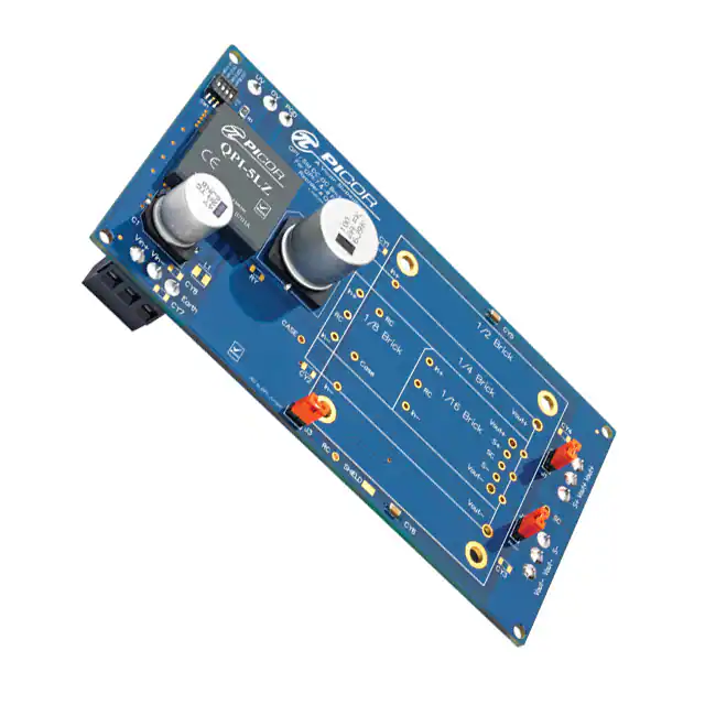
(System‑in‑Package) with LGA mounting. Evaluation boards are
available to allow for quick in-circuit testing of the QPI-5LZ within
an existing system design.
• Connect in series for higher attenuation
• 75dB DM attenuation at 250kHz (50Ω)
• 40VDC (max input)
• 100VDC surge 100ms
• 707VDC hipot hold off to shield plane
• 14A rating
• ~1in2 area
• –40 to +125°C ambient temperature (see Figure 9)
• Efficiency >99%
• TÜV certified
Applications
• Industrial Bus Supplies
• Telecom Base Stations
• IBA & Distributed Power
• COTS Systems
Package Information
• 25.3 x 25.3 x 5.2mm lidded SiP (System-in-Package)
• 24.9 x 24.9 x 4.4mm open-frame SiP
Typical Application
BUS+
BUS+
CB1
BUS–
QPI+
IN+
CIN
QPI-5
BUS–
PR
QPI–
Shield
IN–
CY1
Chassis/Shield
PC
OUT+
SENSE+
LOAD
SC
SENSE–
OUT–
CY2
CY3
CY4
Shield Plane
RY
QPI-5 schematic with a Vicor Brick® converter [a]
[a]
CB1 capacitor, referenced in all schematics, is a 47µF electrolytic; United Chemi-Con EMVE101ARA470MKE0S or equivalent.
CY1 to CY4, referenced in all schematics, are 4.7nF high-voltage safety capacitors; Vishay VY1472M63Y5UQ63V0 or equivalent.
CIN is the manufacturer’s recommended value for input capacitor.
QPI™ Filters
Page 1 of 15
Rev 3.0
03/2020
�QPI-5LZ
Contents
Order Information
3
Absolute Maximum Ratings
3
Electrical Characteristics
3
Package Pinout
4
Applications Information
5
EMI Sources
5
Passive EMI Filtering
5
Active EMI Filtering
5
EMI Management
6
Attenuation Test Set Ups
7
Attenuation Plots
8
Current De-Rating
8
QPI Application Circuits
9
QPI Insertion Loss Measurements and Test Circuits
11
Package Outline Drawings
12
Pad and Stencil Definitions
13
PCB Layout Recommendations
14
PCB Layout
14
Post-Solder Cleaning
14
QPI-5 Mechanical Data
14
Product Warranty
QPI™ Filters
Page 2 of 15
15
Rev 3.0
03/2020
�QPI-5LZ
Order Information
Product
Description
QPI-5LZ [b]
QPI-5 LGA package, RoHS compliant
QPI-5LZ-01
QPI-5 LGA package, RoHS compliant, open-frame package
Evaluation Board
Description
A QPI-5LZ mounted on a small evaluation board with screw terminal blocks to allow for easy connection into an
existing system.
A QPI-5LZ mounted on a carrier board designed for use with DOSA compliant footprint DC-DC converters.
Screw terminal blocks to allow for easy connection into an existing system.
QPI-5-EVAL1
QPI-5-CB1
[b]
QPI-5LZ is a non-hermetically sealed package. Please read the “Post-Solder Cleaning” section on page 14.
Absolute Maximum Ratings
Exceeding these parameters may result in permanent damage to the product.
Name
Rating
Input Voltage, BUS+ to BUS–, Continuous
–40 to 40VDC
Input Voltage, BUS+ to BUS–, 100ms Transient
–100 to 100VDC
BUS+/ BUS– to Shield Pads, Hi-pot
–707 to 707VDC
Input to Output Current, Continuous @ 25°C TA
14ADC
Input-to-Output Current, 10 seconds @ 25°C TA
20ADC
Power Dissipation, @ 65°C TA,
14A [c]
2.3W
Operating Temperature - TA
Thermal
Resistance [c]
–40 to 125°C
- RθJ-A, using PCB layout in Figure 20
20°C/W
Thermal Resistance [c] - RθJ-PCB
8°C/W
Storage Temperature, JEDEC Standard J-STD-033B
–55 to 125°C
Reflow Temperature, 20s Exposure
245°C
ESD, Human Body Model (HBM)
–2000 to 2000V
Electrical Characteristics
Parameter limits apply over the operating temperature range unless otherwise noted.
Parameter
Conditions
Min
Typ
Max
Unit
40
VDC
Measured at 14A, 65°C ambient temperature [c]
135
mVDC
temperature [c]
29
mVDC
BUS+ to BUS– Input Range
Measured at 14A, 65°C ambient temperature [c]
BUS+ to QPI+ Voltage Drop
BUS– to QPI– Voltage Drop
Measured at 14A, 65°C ambient
Common-Mode Attenuation
VBUS = 28V, Frequency = 250kHz, line impedance = 50Ω
60
Differential-Mode Attenuation
VBUS = 28V, Frequency = 250kHz, line impedance = 50Ω
75
dB
Input Bias Current at 40V
Input current from BUS+ to BUS–
8
mA
[c]
See Figure 8 for the current de-rating curve.
QPI™ Filters
Page 3 of 15
Rev 3.0
03/2020
10
dB
�QPI-5LZ
Package Pinout
THERM2
12
BUS+
THERM1
11
10
9
13
8
14
7
15
6
BUS–
QPI+
Shield
16
5
1
2
3
4
QPI–
Pad Number
Name
Description
12, 13, 14
BUS+
Positive bus potential
1, 15, 16
BUS–
Negative bus potential
7, 8, 9
QPI+
Positive input to the converter
2, 3, 4
QPI–
Negative input to the converter
5, 6
Shield
10
THERM1
11
THERM2
QPI™ Filters
Page 4 of 15
Shield connects to the system chassis or to a safety ground
These pads are electrically connected to the internal circuitry of the QPI-5.
Either connecting THERM1 to QPI+ and THERM2 to BUS+, or to copper region(s) not
connected to Shield, is recommended to help with thermal management.
Rev 3.0
03/2020
�QPI-5LZ
Applications Information
Active EMI Filtering
EMI Sources
Many of the components in today’s power conversion modules
are sources of high-frequency EMI noise generation. Diodes,
high‑frequency switching devices, transformers and inductors, and
circuit layouts passing high dV/dt or di/dt signals are all potential
sources of EMI.
The Vicor QPI-5 active EMI filter uses the same basic principles for
filtering as the passive approach, but its active common-mode
filter can perform as well as a passive filter, when filtering lower
frequencies, in much less board area.
CM w/Aux Winding
LDM
EMI is propagated either by radiated or conductive means. Radiated
EMI can be sourced from these components as well as by circuit
loops that act like antennas and broadcast the noise signals to
neighboring circuit paths. This also means that these loops can act
as receivers of a broadcasted signal. This radiated EMI noise can be
reduced by proper circuit layout and by shielding potential sources
of EMI transmission.
There are two basic forms of conducted EMI that typically need
to be filtered; namely common-mode (CM) and differential-mode
(DM) EMI. Differential-mode resides in the normal power loop
of a power source and its load; where the signal travels from the
source to the load and then returns to the source. Common‑mode
is a signal that travels through both leads of the source and is
returned to earth via parasitic pathways, either capacitively or
inductively coupled.
Figure 6 and Figure 7 are the resulting EMI plots, after filtering by
the QPI-5, of the total noise, both common- and differential‑mode,
of a Vicor Brick converter. These converters are mounted on a
QPI-5 evaluation board and tested under various loads. The red and
blue traces represent the positive and negative branches of total
noise, as measured using an industry-standard LISN set up, as is
shown in Figures 4 and 5.
Differential-mode EMI is typically larger in magnitude than
common-mode, since common-mode is produced by the physical
imbalances in the differential loop path. Reducing differential EMI
will cause a reduction in common-mode EMI.
Passive EMI Filtering
The basic premise of filtering EMI is to insert a high impedance
at the EMI’s base frequency, in both the differential- and
common‑mode paths as it returns to the power source.
CDM
Y Caps
Active CM Filter
Figure 1 — Simplified active EMI filter circuit.
Typically, the lower the frequency the greater the needed
inductance would be to properly filter the EMI signal. This means
either a larger core or a greater number of turns on a smaller core.
A larger core requires more board space, where a smaller core with
more turns has a greater amount of unwanted parasitics that can
affect the filters ability to attenuate EMI signals.
Figure 1 is a simplified schematic of the QPI-5’s active and passive
circuitry used for EMI filtering. The QPI-5’s active filter uses a
small high-frequency common-mode transformer to filter the
higher frequencies and adds a sensing element to it so that the
lower‑frequency common-mode signal can be sensed and a
correction signal can be generated and inserted into the shield
connection. By this means, the QPI-5 is capable of providing EMI
filtering of converters in far less space than standard passive filters
and can provide filtering over the entire EN55022 class B range.
Passive filters use common-mode chokes and “Y” capacitors
to filter out common-mode EMI. These chokes are designed to
present a high impedance at the EMI frequency in series with the
return path, and a low impedance path to the earth signal via the
“Y” caps. This network will force the EMI signals to re-circulate
within a confined area and not to propagate to the outside
world. Often two common-mode networks are required to filter
EMI within the frequency span required to pass the EN55022
class B limits.
The other component of the passive filter is the differential LC
network. Again, the inductor is chosen such that it will present
a high impedance in the differential EMI loop at the EMI’s base
frequency. The differential capacitor will then shunt the EMI back
to its source. The QPI-5 was specifically designed to work with
conventional switching frequency converters like Vicor Brick®
products; Micro, Mini and Maxi modules; as well as converters
from various vendors.
QPI™ Filters
Page 5 of 15
Rev 3.0
03/2020
�QPI-5LZ
EMI Management
The more effectively EMI is managed at the source, namely the
power converter, the less EMI attenuation the filter will have to
do. The addition of “Y” capacitors to the input and output power
nodes of the converter will help to limit the amount of EMI that will
propagate to the input source.
The typical application diagram shows the baseplate topology of
re-circulating “Y” caps. Here, CY1 to CY4 are connected to each
power node of the DC‑DC converter, and then are commoned
together on a copper shield plane created under the converter. The
addition of the copper shield plane helps in the containment of the
radiated EMI, converting it back to conducted EMI and shunting it
back to its source.
The RY resistor, connected between the shield plane and the
QPI’s shield pin, provides an impedance that makes the QPI’s
common‑mode noise cancelation signal more effective at removing
the common‑mode noise that would normally return to the shield/
earth connection. It is important when laying out the QPI that
the RY resistor connects to the QPI’s shield pin before making the
connection to earth ground.
In Figure 3, the open-frame topology is shown where the “Y”
capacitors (CY1 and CY2) re-circulate the EMI signals between
the positive input and output, and the negative input and output
nodes of the power‑conversion stage.
Figure 2 — An unfiltered converter’s response to
“open‑frame” (light blue) and “baseplate” (purple)
EMI configurations
There are two basic topologies for the connection of the
re‑circulating “Y” capacitors, referred to as “open-frame” and
“baseplate”. Figure 2 illustrates how a converter can favor one
topology versus another. The EMI generated by the “baseplate”
configuration is much greater than that generated by the
“open‑frame”. Selecting the right topology will greatly reduce the
amount of EMI signal that needs to be filtered.
CY2
BUS+
BUS+
CB1
BUS–
QPI+
CIN
QPI-5
BUS–
IN+
OUT+
SENSE+
PC
SC
PR
QPI–
Shield
SENSE–
OUT–
IN–
Chassis/Shield
CY1
Figure 3 — Typical ‘open-frame’ application
QPI™ Filters
Page 6 of 15
Rev 3.0
03/2020
LOAD
�QPI-5LZ
Attenuation Test Set Ups
Figure 4 — Open-frame EMI test set up using the QPI-5-CB1 carrier board with 24V converter
Figure 5 — Baseplate EMI test set up using the QPI-5-CB1 carrier board with 24V converter
In Figures 4 and 5, C1 is the required 47µF capacitor (United
Chemi‑Con EMVE101ARA470MKE0S or equivalent), C2 is a
converter input cap (value dependant on converter), and CY caps
are 4.7nF ceramic (Murata GRM31BR73A472KW01L or equivalent).
QPI™ Filters
Page 7 of 15
Rev 3.0
03/2020
�QPI-5LZ
Attenuation Plots
Total EMI noise in baseplate configuration, tested as shown in Figure 5.
Figure 6 — V24B24C200BG using baseplate “Y” capacitors
with a 171W load
Figure 7 — V24B12C200BN using baseplate “Y” capacitors
with a 136W load
Current De-Rating
2.5
Maximum Current (A)
20
18
2.0
16
14
1.5
12
10
1.0
8
6
4
0.5
2
0
–40
0.0
–15
0
10
35
60
85
110
Ambient Temperature (ºC)
QPI-5 Current
QPI-5 Power Dissipation
Figure 8 — Current de-rating and power dissipation over ambient temperature range
The de-rating curve in Figure 8 is based on the maximum
allowable internal component temperature and the 14A maximum
rating of the QPI-5. The power dissipation curve is based on the
current squared multiplied by the internal resistance between the
inputs and outputs of the filter. The internal resistance value is
temperature compensated for the power dissipation curve. The
left axis is in amps for the solid trace, the right axis is in watts for
the dashed trace.
QPI™ Filters
Page 8 of 15
Rev 3.0
03/2020
125
Maximum Power Dissipation (W)
Mounted to QPI-5-EVAL1 evaluation board.
�QPI-5LZ
QPI Application Circuits
BUS+
BUS+
QPI+
IN+
CIN1
QPI-5
47µF
BUS–
BUS–
PC
QPI–
SENSE–
OUT–
IN–
CY2
CY1
RY
10Ω, 0.25W
LOAD1
SC
PR
Shield
Chassis/Shield
OUT+
SENSE+
CY4
CY3
Shield Plane
IN+
CIN2
OUT+
SENSE+
PC
SENSE–
OUT–
IN–
CY6
CY5
LOAD2
SC
PR
CY8
CY7
Shield Plane
Figure 9 — The QPI-5 filtering dual supplies, using a single RY resistor [d]
The shield plane under the two converters in Figure 9 should be
one contiguous plane under both. The circuit in Figure 9 is capable
of filtering more converters than shown, up to the maximum
current capability of the QPI-5. In Figure 10, a separate shield plane
is required for each converter along with a separate RY resistor.
BUS+
BUS+
QPI+
IN+
CIN1
QPI-5
47µF
BUS–
The QPI-5 is not designed to be used in parallel with another QPI-5
to achieve a higher current rating, but it can be used multiple times
within a system design.
BUS–
PR
QPI–
Shield
BUS+
CY1
CY2
QPI+
BUS–
CY3
IN+
CIN2
PC
PR
QPI–
Shield
OUT+
SENSE+
SC
SENSE–
OUT–
IN–
RY
10Ω, 0.25W
CY4
OUT–
Shield Plane
QPI-5
47µF
LOAD
SC
SENSE–
IN–
RY
10Ω, 0.25W
Chassis/Shield
PC
OUT+
SENSE+
CY5
CY6
Shield Plane
CY7
CY8
Figure 10 — Dual QPI-5’s filtering paralleled converters feeding a common load [d]
[d]
In Figures 9 and 10; CIN1 and CIN2, CY1 through CY8, should be the value and voltage rating recommended by the converter’s manufacturer.
QPI™ Filters
Page 9 of 15
Rev 3.0
03/2020
�QPI-5LZ
QPI Application Circuits (Cont.)
BUS+
BUS+
CB1
BUS–
QPI+
IN+
CIN
QPI-5
BUS–
SENSE+
PC
SENSE–
OUT–
IN–
CY2
CY1
LOAD
SC
PR
QPI–
Shield
Chassis/Shield
OUT+
CY3
Shield Plane
4.7µH
Figure 11 — Connecting the converter’s output ground to chassis through an inductor [e]
The direct connection of the converter’s output to the earth/chassis
will degrade the EMI attenuation performance of the QPI-5. Vicor
recommends that the connection to the earth be made through
a series inductor, rated to the maximum output current of the
converter, as shown in Figure 11. The EMI plot shown in Figure 12
is of the same converter as in Figure 6, but uses an inductor in
place of RY and has the converter’s output ground connected to
the shield plane.
The connection of the shield plane directly to the chassis/earth
will also degrade EMI attenuation by the QPI-5 and is therefore
not recommended.
Figure 12 — Total noise V24B12C200BN with a 136W load,
connected as shown in Figure 11
[e]
In Figure 12; CIN, CY1 through CY3, should be the value and voltage rating recommended by the converter’s manufacturer.
QPI™ Filters
Rev 3.0
Page 10 of 15 03/2020
�QPI-5LZ
QPI Insertion Loss Measurements and Test Circuits
90
80
Attenuation (dB)
70
60
50
40
30
20
10
0
0.01
0.1
1
10
Frequency (MHz)
QPI-5 Common
QPI-5 Differential
Figure 13 — Attenuation curves into a 50Ω line impedance, bias from a 28V bus
Insertion loss equation:
Insertion Loss = 20log
( )
IINA
IINB
IPROBE
BUS
BUS+
IN
LISN
VBUS
Chassis
47µF
QPI+
QPI-5
SIG
BUS–
INA
INB
QPI–
SIG
50Ω
Shield
BUS
CSIG
LOAD
IN
LISN
Chassis
IPROBE
SIG
Figure 14 — Test set up to measure differential-mode EMI currents in Figure 13
IN
BUS
LISN
VBUS
Chassis
BUS+
47µF
QPI+
QPI-5
SIG
BUS–
QPI–
Shield
BUS
IPROBE
LOAD
INA
CSIG
INB
SIG
IN
50Ω
LISN
Chassis
SIG
Figure 15 — Test set up to measure common-mode EMI currents in Figure 13
QPI™ Filters
Rev 3.0
Page 11 of 15 03/2020
IPROBE
�QPI-5LZ
Package Outline Drawings
Figure 16 — Lidded package dimensions, tolerance of ±0.004in
0.006" [0.15mm] max.
0.006" [0.15mm] max.
0.260" [6.604 mm]
5LZ-01
0.275" [6.985 mm]
0.979" [24.867 mm]
Pin 1
0.979" [24.867 mm]
Figure 17 — Open-frame package dimensions, tolerance of ±0.004in; pick-and-place from label center
QPI™ Filters
Rev 3.0
Page 12 of 15 03/2020
0.174 [4.420 mm]
�QPI-5LZ
Pad and Stencil Definitions
QPI-5 LGA
Pa�ern
(Bo�om View)
QPI-5 PCB
Receptor Pa�ern
(Top View)
0.996" (LID)
0.979" (OF)
0.441
0.441
0.300
0.300
0.100
0.100
Figure 18 — Bottom view of open-frame (OF) and lidded (LID) products (all dimensions are in inches)
45.000°
R0.041
0.145"
0.082"
0.041"
0.000"
0.149"
0.085"
0.043"
0.000"
0.129"
0.073"
0.037"
0.000"
1 place
0.082"
0.041"
0.000"
0.086"
0.043"
0.000"
0.073"
0.037"
0.000"
13 places
0.073"
0.037"
0.000"
2 places
0.082"
0.041"
0.000"
0.1250"
LGA Pad Detail:
R0.043
0.086"
0.043"
0.000"
0.129"
R0.037
0.112"
Receiving Pad Detail:
Stencil Detail:
Figure 19 — Recommended receptor and stencil patterns (all dimensions are in inches)
Note: Stencil definition is based on a 6mil stencil thickness, 80% of LGA pad area coverage.
LGA Package dimensions are for both the open-frame and lidded versions of the QPI-5.
QPI™ Filters
Rev 3.0
Page 13 of 15 03/2020
0.441
0.300
0.441
0.441
0.100
0.300
0.441
0.100
0.441
0 .0 0 0
0.300
0.300
0.300
0.441
0.100
0.100
0.000
0.000
0.996" (LID)
0.100
0.979" (OF)
0.100
0.300
0 .0 0 0
�QPI-5LZ
PCB Layout Recommendations
Figure 20 — 3D view of paralleling planes underneath the QPI-5
PCB Layout
Post-Solder Cleaning
When laying out the QPI-5 EMI filter it is important for the designer
to be aware of the radiated EMI field that all converters emit and
to place the QPI-5 outside of this field area. It is also recommended
that the bus lines feeding into the QPI filter are not routed such
that they lie between the QPI and the converter, or that their
copper planes overlap on inner layers. This can cause EMI noise
to be coupled from input to output via the parasitic capacitance
between the planes.
LZ version QP SiPs are not hermetically sealed and must not be
exposed to liquid, including but not limited to cleaning solvents,
aqueous washing solutions or pressurized sprays. When soldering,
it is recommended that no-clean flux solder be used, as this will
ensure that potentially corrosive mobile ions will not remain on,
around, or under the module following the soldering process. For
applications where the end product must be cleaned in a liquid
solvent, Vicor recommends using the QPI-5LZ-01, open-frame
version of the EMI filter.
In Figure 20, the QPI-5 is located ~1.5 inches from the converter’s
input pins, and the BUS voltage pins are located on the side
farthest away from the converter, to keep the radiated EMI from
bypassing the filter and coupling directly to the BUS feeds.
QPI-3 Mechanical Data
Datum
FITS
MTBF
Weight
Units
QPI-5LZ
QPI-5LZ-01
Failure/Billion Hrs
208
208
FITS based on the BellCore Standard TR-332
Million Hrs
4.81
4.81
MTBFs based on the BellCore Standard TR-332
grams
5.4
3.1
3
3
245
245
MSL
Peak Reflow Temperature
°C/20 seconds
QPI™ Filters
Rev 3.0
Page 14 of 15 03/2020
Notes
IPC/JEDEC J-STD-020D
�QPI-5LZ
Vicor’s comprehensive line of power solutions includes high density AC-DC and DC-DC modules and
accessory components, fully configurable AC-DC and DC-DC power supplies, and complete custom
power systems.
Information furnished by Vicor is believed to be accurate and reliable. However, no responsibility is assumed by Vicor for its use. Vicor makes
no representations or warranties with respect to the accuracy or completeness of the contents of this publication. Vicor reserves the right
to make changes to any products, specifications, and product descriptions at any time without notice. Information published by Vicor has
been checked and is believed to be accurate at the time it was printed; however, Vicor assumes no responsibility for inaccuracies. Testing
and other quality controls are used to the extent Vicor deems necessary to support Vicor’s product warranty. Except where mandated by
government requirements, testing of all parameters of each product is not necessarily performed.
Specifications are subject to change without notice.
Visit http://www.vicorpower.com/dc-dc-filters/qpi for the latest product information.
Vicor’s Standard Terms and Conditions and Product Warranty
All sales are subject to Vicor’s Standard Terms and Conditions of Sale, and Product Warranty which are available on Vicor’s webpage
(http://www.vicorpower.com/termsconditionswarranty) or upon request.
Life Support Policy
VICOR’S PRODUCTS ARE NOT AUTHORIZED FOR USE AS CRITICAL COMPONENTS IN LIFE SUPPORT DEVICES OR SYSTEMS WITHOUT THE
EXPRESS PRIOR WRITTEN APPROVAL OF THE CHIEF EXECUTIVE OFFICER AND GENERAL COUNSEL OF VICOR CORPORATION. As used
herein, life support devices or systems are devices which (a) are intended for surgical implant into the body, or (b) support or sustain life and
whose failure to perform when properly used in accordance with instructions for use provided in the labeling can be reasonably expected to
result in a significant injury to the user. A critical component is any component in a life support device or system whose failure to perform
can be reasonably expected to cause the failure of the life support device or system or to affect its safety or effectiveness. Per Vicor Terms
and Conditions of Sale, the user of Vicor products and components in life support applications assumes all risks of such use and indemnifies
Vicor against all liability and damages.
Intellectual Property Notice
Vicor and its subsidiaries own Intellectual Property (including issued U.S. and Foreign Patents and pending patent applications) relating to the
products described in this data sheet. No license, whether express, implied, or arising by estoppel or otherwise, to any intellectual property
rights is granted by this document. Interested parties should contact Vicor’s Intellectual Property Department.
The products described on this data sheet are protected by U.S. Patents. Please see www.vicorpower.com/patents for the latest
patent information.
Contact Us: http://www.vicorpower.com/contact-us
Vicor Corporation
25 Frontage Road
Andover, MA, USA 01810
Tel: 800-735-6200
Fax: 978-475-6715
www.vicorpower.com
email
Customer Service: custserv@vicorpower.com
Technical Support: apps@vicorpower.com
©2020 Vicor Corporation. All rights reserved. The Vicor name is a registered trademark of Vicor Corporation.
PICMG® is a trademark of the PICMG consortium.
All other trademarks, product names, logos and brands are property of their respective owners.
QPI™ Filters
Rev 3.0
Page 15 of 15 03/2020
�