SFH618A/628A
Phototransistor, 5.3 kV TRIOS Low Current Input Optocoupler
FEATURES • Very High CTR at IF=1.0 mA, VCE=0.5 V – SFH618A-2, 63–125% – SFH618A-3, 100–200% – SFH618A-4, 160–320% – SFH618A-5, 250–500% – SFH628A-2, 63–200% – SFH628A-3, 100–320% – SFH628A-4, 160–500% • Specified Minimum CTR at IF=0.5 mA – SFH618A, VCE=1.5 V: ≥32% (typical 120%) – SFH628A, VCE=1.5 V: ≥50% (typical 160%) • Good CTR Linearity Depending on Forward Current • Low CTR Degradation • High Collector-emitter Voltage, VCEO=55 V • Isolation Test Voltage, 5300 VRMS • Low Coupling Capacitance • Field-Effect Stable by TRIOS (TRansparent IOn Shield) • End-Stackable, 0.100" (2.54 mm) Spacing • High Common-mode Interference Immunity (Unconnected Base) • Underwriters Lab File #52744 • V VDE 0884 Available with Option 1 • SMD Option — See SFH6186/6286 Data Sheet
DE
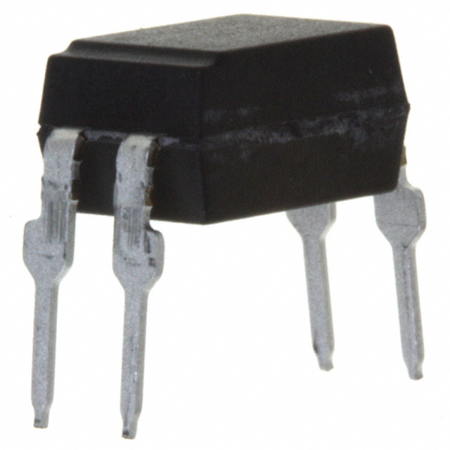
Dimensions in Inches (mm)
2 1 pin one ID .255 (6.48) .268 (6.81)
Anode 1 Cathode 2 SFH628A Anode/ Cathode 1 SFH618A
4 Collector 3 Emitter
4 Collector 3 Emitter
3
4
Cathode/ Anode 2
.179 (4.55) .190 (4.83) .030 (.76) .045 (1.14) .031 (.79) typ. .050 (1.27) typ. .130 (3.30) .150 (3.81) 4° typ. .018 (.46) .022 (.56)
.300 (7.62) typ.
10° .020 (.508 ) .035 (.89) .050 (1.27) 0.100 (2.54) 3°–9° .008 (.20) .012 (.30)
.230 (5.84) .250 (6.35) .110 (2.79) .130 (3.30)
APPLICATIONS • Telecom • Industrial Controls • Battery Powered Equipment • Office Machines DESCRIPTION The SFH618A/628A feature a high current transfer ratio, low coupling capacitance and high isolation voltage. These couplers have a GaAs infrared emitting diode emitter, which is optically coupled to a silicon planar phototransistor detector, and is incorporated in a plastic DIP-4 package. The coupling devices are designed for signal transmission between two electrically separated circuits. The couplers are end-stackable with 2.54 mm lead spacing. Creepage and clearance distances of >8.0 mm are achieved with option 6. This version complies with IEC 950 (DIN VDE 0805) for reinforced insulation up to an operation voltage of 400 VRMS or DC.
Maximum Ratings Emitter Reverse Voltage (SFH618A)............................................................. 6.0 V DC Forward Current (SFH628A) .................................................. ±50 mA Surge Forward Current (tp≤10 µs) (SFH628A) ............................... ±2.5 A Total Power Dissipation ................................................................. 70 mW Detector Collector-emitter Voltage ................................................................... 55 V Emitter-collector Voltage................................................................... 7.0 V Collector Current ............................................................................ 50 mA Collector Current (tp≤1.0 ms) ....................................................... 100 mA Total Power Dissipation ............................................................... 150 mW Package Isolation Test Voltage between Emitter and Detector, refer to Climate DIN 40046, part 2, Nov. 74 ..................................................................... 5300 VRMS Creepage Distance .................................................................... ≥7.0 mm Clearance ................................................................................... ≥7.0 mm Insulation Thickness between Emitter and Detector .................. ≥0.4 mm Comparative Tracking Index per DIN IEC 112/VDE0 303, part 1 ..................................................175 Isolation Resistance VIO=500 V, TA=25°C ................................................................. ≥1012 Ω VIO=500 V, TA=100°C ............................................................... ≥1011 Ω Storage Temperature Range ............................................. –55 to +150°C Ambient Temperature Range............................................. –55 to +100°C Junction Temperature ......................................................................100°C Soldering Temperature (max. 10 s. Dip Soldering Distance to Seating Plane ≥1.5 mm) ..........................................260°C
www.vishay.com
2–242
Document Number: 83673 Revision 17-August-01
�Characteristics (TA=25°C)
Description Emitter Forward Voltage Reverse Current Capacitance Thermal Resistance Detector Collector-emitter Leakage Current Capacitance Thermal Resistance Package Collector-emitter Saturation Voltage SFH618A-2 SFH618A-3 SFH618A-4 SFH618A-5 Collector-emitter Saturation Voltage SFH628A-2 SFH628A-3 SFH628A-4 Coupling Capacitance Coupling Transfer Ratio — SFH618A-2 SFH618A-2 SFH618A-3 SFH618A-3 SFH618A-4 SFH618A-4 SFH618A-5 SFH618A-5 Coupling Transfer Ratio SFH628A-2 SFH628A-2 SFH628A-3 SFH628A-3 SFH628A-4 SFH628A-4 I C / IF I C / IF I C / IF I C / IF I C / IF I C / IF CC I C / IF VCEsat VCEsat — — — — — — — — 63 32 100 50 160 80 250 125 63 32 100 50 160 80 0.25 0.25 0.25 0.25 0.25 0.25 0.25 0.25 — 75 — 120 — 200 — 300 — 100 — 160 — 250 0.4 0.4 0.4 0.4 0.4 0.4 0.4 — 125 — 200 — 320 — 500 — 200 — 320 — 500 — % % % % % % pF % V V IC=0.32 mA, IF=1.0 mA IC=0.5 mA, IF=1.0 mA IC=0.8 mA, IF=1.0 mA IC=1.25 mA, IF=1.0 mA IC=0.5 mA, IF=±1.0 mA IC=0.8 mA, IF=±1.0 mA IC=1.25 mA, IF=±1.0 mA — IF=1.0 mA, VCE=0.5 V IF=0.5 mA, VCE=1.5 V IF=1.0 mA, VCE=0.5 V IF=0.5 mA, VCE=1.5 V IF=1.0 mA, VCE=0.5 V IF=0.5 mA, VCE=1.5 V IF=1.0 mA, VCE=0.5 V IF=0.5 mA, VCE=1.5 V IF=±1.0 mA, VCE=0.5 V IF=±0.5 mA, VCE=1.5 V IF=±1.0 mA, VCE=0.5 V IF=±0.5 mA, VCE=1.5 V IF=±1.0 mA, VCE=0.5 V IF=±0.5 mA, VCE=1.5 V ICEO CCE RthJA — — — 10 7 500 200 — — nA pF K/W VCE=10 V VCE=5.0 V, f=1.0 MHz — SFH618A SFH618A SFH628A VF IR C0 RthJA — — — — 1.1 .01 25 45 1070 1.5 10 — — V µA pF K/W IF=5.0 mA VR=6.0 V VR=0 V, f=1.0 MHz — Symbol Min. Typ. Max. Unit Condition
Document Number: 83673 Revision 17-August-01
www.vishay.com
2–243
�Figure 1. Current Transfer Ratio (typ.) VCE=0.5 V, CTR=f(TA)
Figure 4. Diode Forward Voltage IF=1.0 mA, VF=f(TA)
Figure 7. Permissible Forward Current Diode IF=f(TA)
Figure 2. Current Transfer Ratio (typ.) VCE=1.5 V, CTR=f(TA)
Figure 5. Transistor Capacitance TA=25°C, f=1.0 MHz, CCE=f(VCE)
Figure 8. Permissible Power Dissipation Ptot=f(TA)
Figure 3. Diode Forward Voltage TA=25°C, VF=f(IF)
Figure 6. Output Characteristics TA=25°C, CE=f(VCE, IF)
Figure 9. Switching Times (typ.) TA=25°C, IF=1.0 mA, VCC=5.0 V ton, tr, toff, tf=f(RL)
Document Number: 83673 Revision 17-August-01
www.vishay.com
2–244
�Switching Times, typical VCC=5.0 V, IC=2.0 mA, RL=100 Ω, TA=25°C Turn-on Time Rise Time Turn-off Time Fall Time ton tr toff tf 6.0 3.5 5.5 5.0 µs
Figure 11. Test Circuit—SFH628A
±IF RL VCC IC
47Ω
Figure 10. Test Circuit—SFH618A Figure 12. Test Circuit and Waveforms VCC = 5 V Input RL VOUT
Input Pulse 10% 90% tr ton tf toff Output Pulse
Document Number: 83673 Revision 17-August-01
www.vishay.com
2–245
�