Si2301BDS
Vishay Siliconix
P-Channel 2.5-V (G-S) MOSFET
PRODUCT SUMMARY
VDS (V)
- 20
rDS(on) (W)
0.100 @ VGS = - 4.5 V 0.150 @ VGS = - 2.5 V
ID (A)b
- 2.4 - 2.0
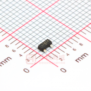
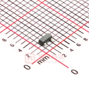
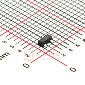
TO-236 (SOT-23)
G
1 3 D Ordering Information: Si2301BDS-T1
S
2
Top View Si2301 BDS (L1)* *Marking Code
ABSOLUTE MAXIMUM RATINGS (TA = 25_C UNLESS OTHERWISE NOTED)
Parameter
Drain-Source Voltage Gate-Source Voltage Continuous Drain Current (TJ = 150_C)b Pulsed Drain Currenta Continuous Source Current (Diode Conduction)b Power Dissipationb Operating Junction and Storage Temperature Range TA= 25_C TA= 70_C TA= 25_C TA= 70_C
Symbol
VDS VGS ID IDM IS PD TJ, Tstg
5 sec
- 20 "8 - 2.4 - 1.9 - 10 - 0.72 0.9 0.57
Steady State
Unit
V
- 2.2 - 1.8 A
- 0.6 0.7 0.45 - 55 to 150 W _C
THERMAL RESISTANCE RATINGS
Parameter
Maximum Junction-to-Ambientb Maximum Junction-to-Ambientc Notes a. Pulse width limited by maximum junction temperature. b. Surface Mounted on FR4 Board, t v 5 sec. c. Surface Mounted on FR4 Board. For SPICE model information via the Worldwide Web: http://www.vishay.com/www/product/spice.htm Document Number: 72066 S-31990—Rev. B, 13-Oct-03 www.vishay.com RthJA
Symbol
Typical
120 140
Maximum
145 175
Unit
_C/W
1
�Si2301BDS
Vishay Siliconix
SPECIFICATIONS (TJ = 25_C UNLESS OTHERWISE NOTED)
Limits Parameter Static
Drain-Source Breakdown Voltage Gate-Threshold Voltage Gate-Body Leakage Zero Gate Voltage Drain Current V(BR)DSS VGS(th) IGSS IDSS VGS = 0 V, ID = - 250 mA VDS = VGS, ID = - 250 mA VDS = 0 V, VGS = "8 V VDS = - 20 V, VGS = 0 V VDS = - 20 V, VGS = 0 V, TJ = 55_C VDS v - 5 V, VGS = - 4.5 V VDS v - 5 V, VGS = - 2.5 V VGS = - 4.5 V, ID = - 2.8 A VGS = - 2.5 V, ID = - 2.0 A VDS = - 5 V, ID = - 2.8 A IS = - 0.75 A, VGS = 0 V -6 -3 0.080 0.110 6.5 - 0.80 - 1.2 0.100 0.150 - 20 - 0.45 - 0.95 "100 -1 - 10 V nA mA
Symbol
Test Conditions
Min
Typ
Max
Unit
On-State On State Drain Currenta
ID( ) D(on)
A
Drain-Source On-Resistance Drain Source On Resistancea Forward Transconductancea Diode Forward Voltage
rDS( ) DS(on) gfs VSD
W S V
Dynamicb
Total Gate Charge Gate-Source Charge Gate-Drain Charge Input Capacitance Output Capacitance Reverse Transfer Capacitance Qg Qgs Qgd Ciss Coss Crss VDS = - 6 V, VGS = 0, f = 1 MHz VDS = - 6 V, VGS = - 4.5 V ID ^ - 2.8 A 2.8 4.5 0.7 1.1 375 95 65 pF 10 nC
Switchingc
Turn-On Turn On Time td(on) tr td(off) tf VDD = - 6 V, RL = 6 W ID ^ - 1.0 A, VGEN = - 4.5 V 45 RG = 6 W 20 40 30 20 30 60 45 30 ns
TurnTurn-Off Time Time
Notes a. Pulse test: PW v300 ms duty cycle v2%. b. For DESIGN AID ONLY, not subject to production testing. c. Switching time is essentially independent of operating temperature. S FaxBack 408-970-5600
www.vishay.com
2
Document Number: 72066 S-31990—Rev. B, 13-Oct-03
�Si2301BDS
Vishay Siliconix
TYPICAL CHARACTERISTICS (25_C UNLESS NOTED)
10
Output Characteristics
10
Transfer Characteristics
8 I D - Drain Current (A)
VGS = 5 thru 2.5 V I D - Drain Current (A)
8 2V
TC = - 55_C
6
6
25_C
125_C
4 1.5 V 2 1V 0 0 1 2 3 4 5 VDS - Drain-to-Source Voltage (V)
4
2
0 0.0
0.5
1.0
1.5
2.0
2.5
3.0
VGS - Gate-to-Source Voltage (V)
0.5
On-Resistance vs. Drain Current
800
Capacitance
r DS(on)- On-Resistance ( W )
0.4 C - Capacitance (pF)
600
0.3
400
Ciss
0.2
VGS = 2.5 V
0.1 VGS = 4.5 V 0.0 0 2 4 6 8 10 ID - Drain Current (A)
200
Coss Crss 0 4 8 12 16 20
0
VDS - Drain-to-Source Voltage (V)
5 VDS = 10 V ID = 2.8 A V GS - Gate-to-Source Voltage (V) 4
Gate Charge
1.6
On-Resistance vs. Junction Temperature
VGS = 4.5 V ID = 2.8 A
1.4 r DS(on)- On-Resistance ( W ) (Normalized) 0 1 2 3 4 5
3
1.2
2
1.0
1
0.8
0
0.6 - 50
- 25
0
25
50
75
100
125
150
Qg - Total Gate Charge (nC)
TJ - Junction Temperature (_C)
Document Number: 72066 S-31990—Rev. B, 13-Oct-03
www.vishay.com
3
�Si2301BDS
Vishay Siliconix
TYPICAL CHARACTERISTICS (25_C UNLESS NOTED)
10
Source-Drain Diode Forward Voltage
0.6 0.5
On-Resistance vs. Gate-to-Source Voltage
TJ = 150_C
r DS(on)- On-Resistance ( W )
I S - Source Current (A)
0.4 ID = 2.8 A 0.3 0.2 0.1 0.0
1 TJ = 25_C
0.1 0 0.2 0.4 0.6 0.8 1.0 1.2 VSD - Source-to-Drain Voltage (V)
0
1
2
3
4
5
VGS - Gate-to-Source Voltage (V)
0.4 0.3 V GS(th) Variance (V) 0.2
Threshold Voltage
10
Single Pulse Power
8
ID = 250 mA 0.1 0.0 - 0.1 - 0.2 - 50
Power (W)
6
4 TA = 25_C 2
0 - 25 0 25 50 75 100 125 150 0.01 0.1 1 10 100 1000 TJ - Temperature (_C) 100 Time (sec)
Safe Operating Area
10 I D - Drain Current (A)
10 ms 100 ms
1
1 ms 10 ms 100 ms dc, 100 s, 10 s, 1 s
0.1
TA = 25_C Single Pulse
0.01 0.1 1 10 100 VDS - Drain-to-Source Voltage (V) Square Wave Pulse Duration (sec) www.vishay.com Document Number: 72066 S-31990—Rev. B, 13-Oct-03
4
�Si2301BDS
Vishay Siliconix
TYPICAL CHARACTERISTICS (25_C UNLESS NOTED)
2 1 Normalized Effective Transient Thermal Impedance
Normalized Thermal Transient Impedance, Junction-to-Ambient
Duty Cycle = 0.5
0.2
Notes:
0.1
0.1 0.05 0.02
PDM t1
t2 1. Duty Cycle, D =
2. Per Unit Base = RthJA = 62.5_C/W
t1 t2
Single Pulse 0.01 10 -4 10 -3 10 -2 10 -1 1
3. TJM - TA = PDMZthJA(t) 4. Surface Mounted
10
100
600
Square Wave Pulse Duration (sec) Document Number: 72066 S-31990—Rev. B, 13-Oct-03 www.vishay.com
5
�
很抱歉,暂时无法提供与“SI2301BDS-T1”相匹配的价格&库存,您可以联系我们找货
免费人工找货- 国内价格
- 1+0.91787
- 10+0.89719
- 30+0.88337
- 100+0.85216
- 国内价格
- 1+1.61608
- 10+1.45255
- 50+1.32173
- 150+1.23451
- 300+1.18
- 国内价格
- 1+0.3248
- 10+0.3045
- 50+0.27405
- 150+0.25375
- 300+0.23954
- 500+0.23345