Si4848DY
Vishay Siliconix
N-Channel 150-V (D-S) MOSFET
PRODUCT SUMMARY
VDS (V)
150
rDS(on) (W)
0.085 @ VGS = 10 V 0.095 @ VGS = 6.0 V
ID (A)
3.7 3.5
D
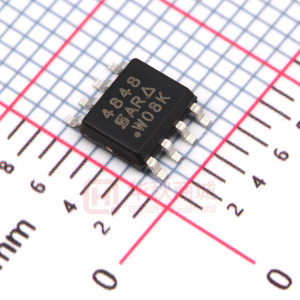
SO-8
S S S G 1 2 3 4 Top View Ordering Information: Si4848DY Si4848DY-T1 (with Tape and Reel) 8 7 6 5 D D D D S N-Channel MOSFET G
ABSOLUTE MAXIMUM RATINGS (TA = 25_C UNLESS OTHERWISE NOTED)
Parameter
Drain-Source Voltage Gate-Source Voltage Continuous Drain Current (TJ = 150_C)a Pulsed Drain Current Avalanch Current Continuous Source Current (Diode Conduction)a Maximum Power Dissipationa Operating Junction and Storage Temperature Range TA = 25_C TA = 70_C L = 0.1 mH TA = 25_C TA = 70_C
Symbol
VDS VGS
10 secs
150 "20 3.7
Steady State
Unit
V
2.7 2.1 25 10 A
ID IDM IAS IS PD TJ, Tstg
3.0
2.5 3.0 1.9 -55 to 150
1.3 1.5 1.0 W _C
THERMAL RESISTANCE RATINGS
Parameter
t v 10 sec Maximum J Mi Junction-to-Ambienta ti t A bi t Maximum Junction-to-Foot (Drain) Notes a. Surface Mounted on 1” x 1” FR4 Board. Document Number: 71356 S-03950—Rev. B, 26-May-03 www.vishay.com Steady State Steady State RthJA RthJF
Symbol
Typical
35 68 18
Maximum
42 82 23
Unit
_C/W
1
�Si4848DY
Vishay Siliconix
SPECIFICATIONS (TJ = 25_C UNLESS OTHERWISE NOTED)
Parameter Static
Gate Threshold Voltage Gate-Body Leakage Zero Gate Voltage Drain Current On-State Drain Currenta VGS(th) IGSS IDSS ID(on) VDS = VGS, ID = 250 mA VDS = 0 V, VGS = "20 V VDS = 120 V, VGS = 0 V VDS = 120 V, VGS = 0 V, TJ = 55_C VDS w 5 V, VGS = 10 V VGS = 10 V, ID = 3.5 A rDS( ) DS(on) VGS = 6.0 V, ID = 3.0 A Forward Transconductancea Diode Forward Voltagea gfs VSD VDS = 15 V, ID = 5 A IS = 2.5 A, VGS = 0 V 25 0.068 0.076 15 0.75 1.2 0.085 0.095 W S V 2.0 "100 1 5 V nA mA A
Symbol
Test Condition
Min
Typ
Max
Unit
Drain-Source On-State Drain Source On State Resistancea
Dynamicb
Total Gate Charge Gate-Source Charge Gate-Drain Charge Gate Resistance Turn-On Delay Time Rise Time Turn-Off Delay Time Fall Time Source-Drain Reverse Recovery Time Qg Qgs Qgd Rg td(on) tr td(off) tf trr IF = 2.5 A, di/dt = 100 A/ms VDD = 75 V, RL = 21 W V, ID ^ 3.5 A, VGEN = 10 V, RG = 6 W 0.5 VDS = 75 V, VGS = 10 V, ID = 3.5 A 17 3.2 6.0 0.85 9.0 10 24 17 45 1.8 14 15 35 25 70 ns W 21 nC
Notes a. Pulse test; pulse width v 300 ms, duty cycle v 2%. b. Guaranteed by design, not subject to production testing.
TYPICAL CHARACTERISTICS (25_C UNLESS NOTED)
Output Characteristics
25 VGS = 10 thru 6 V 20 I D - Drain Current (A) I D - Drain Current (A) 20 25
Transfer Characteristics
15 5V 10
15
10 TC = 125_C 5 25_C
5 3, 4 V 0 0 2 4 6 8 10
0 0 1 2 3 4
-55_C 5 6
VDS - Drain-to-Source Voltage (V) www.vishay.com
VGS - Gate-to-Source Voltage (V) Document Number: 71356 S-03950—Rev. B, 26-May-03
2
�Si4848DY
Vishay Siliconix
TYPICAL CHARACTERISTICS (25_C UNLESS NOTED)
On-Resistance vs. Drain Current
0.15 r DS(on) - On-Resistance ( W ) 1200
Capacitance
C - Capacitance (pF)
0.12
900
Ciss
0.09
VGS = 6 V
600
0.06 VGS = 10 V 0.03
300 Crss Coss 0.00 0 5 10 15 20 25 0 0 30 60 90 120 150
ID - Drain Current (A)
VDS - Drain-to-Source Voltage (V)
Gate Charge
20 V GS - Gate-to-Source Voltage (V) VDS = 75 V ID = 3.5 A 16 3.0
On-Resistance vs. Junction Temperature
VGS = 10 V ID = 3.5 A
r DS(on) - On-Resistance ( W) (Normalized) 12 18 24 30
2.5
2.0
12
1.5
8
1.0
4
0.5
0 0 6 Qg - Total Gate Charge (nC)
0.0 -50
-25
0
25
50
75
100
125
150
TJ - Junction Temperature (_C)
Source-Drain Diode Forward Voltage
50 0.25
On-Resistance vs. Gate-to-Source Voltage
r DS(on) - On-Resistance ( W )
0.20 ID = 3.5 A 0.15
I S - Source Current (A)
TJ = 150_C 10
0.10
TJ = 25_C
0.05
1 0.0
0.00 0.2 0.4 0.6 0.8 1.0 1.2 0 2 4 6 8 10 VSD - Source-to-Drain Voltage (V) VGS - Gate-to-Source Voltage (V)
Document Number: 71356 S-03950—Rev. B, 26-May-03
www.vishay.com
3
�Si4848DY
Vishay Siliconix
TYPICAL CHARACTERISTICS (25_C UNLESS NOTED)
Threshold Voltage
1.0 60 50 0.5 V GS(th) Variance (V) ID = 250 mA 40 0.0 Power (W)
Single Pulse Power
30 20
-0.5
-1.0
10
-1.5 -50
-25
0
25
50
75
100
125
150
0 0.01
0.1
1 Time (sec)
10
100
TJ - Temperature (_C)
Normalized Thermal Transient Impedance, Junction-to-Ambient
2 1 Normalized Effective Transient Thermal Impedance Duty Cycle = 0.5
0.2
Notes:
0.1 0.1 0.05
t1 PDM
0.02
t2 1. Duty Cycle, D =
2. Per Unit Base = RthJA = 68_C/W
t1 t2
Single Pulse 0.01 10 - 4 10 - 3 10 - 2 10 - 1 1 Square Wave Pulse Duration (sec)
3. TJM - TA = PDMZthJA(t) 4. Surface Mounted
10
100
600
Normalized Thermal Transient Impedance, Junction-to-Foot
2 1 Normalized Effective Transient Thermal Impedance Duty Cycle = 0.5
0.2 0.1 0.1 0.05 0.02
Single Pulse 0.01 10 - 4 10 - 3 10 - 2 10 - 1 1 Square Wave Pulse Duration (sec) 10 100 1000
www.vishay.com
4
Document Number: 71356 S-03950—Rev. B, 26-May-03
�
很抱歉,暂时无法提供与“SI4848DY”相匹配的价格&库存,您可以联系我们找货
免费人工找货- 国内价格
- 1+3.6974
- 30+3.56535
- 100+3.4333
- 500+3.1692
- 1000+3.03715
- 2000+2.95792
- 国内价格
- 1+4.018
- 10+3.283
- 30+2.9106