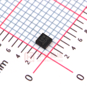
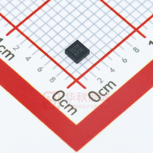
New Product
SiA519EDJ
Vishay Siliconix
N- and P-Channel 20-V (D-S) MOSFET
PRODUCT SUMMARY
VDS (V) N-Channel 20 RDS(on) (Ω) 0.040 at VGS = 4.5 V 0.065 at VGS = 2.5 V 0.090 at VGS = - 4.5 V 0.137 at VGS = - 2.5 V ID (A) 4.5
a
FEATURES
Qg (Typ.) 3.7 nC
4.5a - 4.5a - 4.5a
P-Channel
- 20
5.3 nC
• Halogen-free According to IEC 61249-2-21 Definition • TrenchFET® Power MOSFETs • Typical ESD Protection: N-Channel 2000 V P-Channel 1900 V • 100 % Rg Tested • Compliant to RoHS Directive 2002/95/EC
PowerPAK® SC-70-6 Dual
APPLICATIONS
• Load Switch for Portable Devices • DC/DC Converters
D1 S2
S1 D1 D1 6 5 2.05 mm G2 4
1 2 G1 3 D2 D2 EGX
Marking Code
Part # code
G1 G2
S2
2.05 mm
XXX Lot Traceability and Date code
S1
D2 P-Channel MOSFET
Ordering Information: SiA519EDJ-T1-GE3 (Lead (Pb)-free and Halogen-free)
N-Channel MOSFET
ABSOLUTE MAXIMUM RATINGS TA = 25 °C, unless otherwise noted
Parameter Drain-Source Voltage Gate-Source Voltage TC = 25 °C TC = 70 °C TA = 25 °C TA = 70 °C TC = 25 °C TA = 25 °C TC = 25 °C TC = 70 °C TA = 25 °C TA = 70 °C Symbol VDS VGS ID IDM IS N-Channel 20 ± 12 4.5a 4.5a 4.5a, b, c 4.4b, c 15 4.5a 1.6b, c 7.8 5 1.9b, c 1.2b, c - 55 to 150 260 - 4.5a - 4.5a - 3.7b, c - 3b, c - 15 - 4.5a - 1.6b, c 7.8 5 1.9b, c 1.2b, c A P-Channel - 20 Unit V
Continuous Drain Current (TJ = 150 °C) Pulsed Drain Current Source Drain Current Diode Current
Maximum Power Dissipation
PD TJ, Tstg
W
Operating Junction and Storage Temperature Range Soldering Recommendations (Peak Temperature)d, e
°C
THERMAL RESISTANCE RATINGS
N-Channel Parameter Symbol RthJA RthJC Typ. Max. P-Channel Typ. Max. Unit
t≤5s 52 65 52 65 Maximum Junction-to-Ambientb, f °C/W Maximum Junction-to-Case (Drain) Steady State 12.5 16 12.5 16 Notes: a. Package Limited. b. Surface Mounted on 1" x 1" FR4 board. c. t = 5 s. d. See Solder Profile (www.vishay.com/ppg?73257). The PowerPAK SC-70 is a leadless package. The end of the lead terminal is exposed copper (not plated) as a result of the singulation process in manufacturing. A solder fillet at the exposed copper tip cannot be guaranteed and is not required to ensure adequate bottom side solder interconnection. e. Rework Conditions: manual soldering with a soldering iron is not recommended for leadless components. f. Maximum under Steady State conditions is 110 °C/W. Document Number: 65176 S09-2685-Rev. B, 14-Dec-09 www.vishay.com 1
�New Product
SiA519EDJ
Vishay Siliconix
SPECIFICATIONS TJ = 25 °C, unless otherwise noted
Parameter Static Drain-Source Breakdown Voltage VDS Temperature Coefficient VGS(th) Temperature Coefficient Gate Threshold Voltage VDS ΔVDS/TJ ΔVGS(th)/TJ VGS(th) VGS = 0 V, ID = 250 µA VGS = 0 V, ID = - 250 µA ID = 250 µA ID = - 250 µA ID = 250 µA ID = - 250 µA VDS = VGS, ID = 250 µA VDS = VGS, ID = - 250 µA VDS = 0 V, VGS = ± 4.5 V Gate-Body Leakage IGSS VDS = 0 V, VGS = ± 12 V VDS = 20 V, VGS = 0 V Zero Gate Voltage Drain Current IDSS VDS = - 20 V, VGS = 0 V VDS = 20 V, VGS = 0 V, TJ = 55 °C VDS = - 20 V, VGS = 0 V, TJ = 55 °C On-State Drain Currentb ID(on) VDS ≥ 5 V, VGS = 4.5 V VDS ≤ - 5 V, VGS = - 4.5 V VGS = 4.5 V, ID = 4.2 A Drain-Source On-State Resistanceb RDS(on) VGS = - 4.5 V, ID = - 2.9 A VGS = 2.5 V, ID = 3.3 A VGS = - 2.5 V, ID = - 2.3 A Forward Transconductanceb Dynamica Input Capacitance Output Capacitance Reverse Transfer Capacitance Ciss Coss Crss P-Channel VDS = - 10 V, VGS = 0 V, f = 1 MHz VDS = 10 V, VGS = 10 V, ID = 5.5 A Total Gate Charge Qg VDS = - 10 V, VGS = - 10 V, ID = - 3.7 A N-Channel VDS = 10 V, VGS = 4.5 V, ID = 5.5 A Gate-Source Charge Gate-Drain Charge Gate Resistance Qgs Qgd Rg P-Channel VDS = - 10 V, VGS = - 4.5 V, ID = - 3.7 A f = 1 MHz N-Ch N-Channel VDS = 10 V, VGS = 0 V, f = 1 MHz P-Ch N-Ch P-Ch N-Ch P-Ch N-Ch P-Ch N-Ch P-Ch N-Ch P-Ch N-Ch P-Ch N-Ch P-Ch 0.7 0.2 350 340 82 105 50 95 7.7 10.5 3.7 5.3 0.85 0.75 0.95 2 3.5 10 7 20 Ω 12 16 6 8 nC pF gfs VDS = 10 V, ID = 4.2 A VDS = - 10 V, ID = - 2.9 A N-Ch P-Ch N-Ch P-Ch N-Ch P-Ch N-Ch P-Ch N-Ch P-Ch N-Ch P-Ch N-Ch P-Ch N-Ch P-Ch N-Ch P-Ch N-Ch P-Ch N-Ch P-Ch N-Ch P-Ch 10 - 10 0.032 0.074 0.053 0.113 12 7 0.040 0.090 0.065 0.137 S Ω 0.6 - 0.5 20 - 20 23 - 11 - 3.3 2.6 1.4 - 1.3 ± 0.5 ± 0.5 ± 90 ±8 1 -1 10 - 10 A µA V mV/°C V Symbol Test Conditions Min. Typ. Max. Unit
Notes: a. Guaranteed by design, not subject to production testing. b. Pulse test; pulse width ≤ 300 µs, duty cycle ≤ 2 %.
www.vishay.com 2
Document Number: 65176 S09-2685-Rev. B, 14-Dec-09
�New Product
SiA519EDJ
Vishay Siliconix
SPECIFICATIONS TJ = 25 °C, unless otherwise noted
Parameter Dynamica Turn-On Delay Time Rise Time Turn-Off Delay Time Fall Time Turn-On Delay Time Rise Time Turn-Off Delay Time Fall Time Drain-Source Body Diode Characteristics Continuous Source-Drain Diode Current Pulse Diode Forward Currenta Body Diode Voltage Body Diode Reverse Recovery Time Body Diode Reverse Recovery Charge Reverse Recovery Fall Time Reverse Recovery Rise Time IS ISM VSD trr Qrr ta tb N-Channel IF = 4.4 A, dI/dt = 100 A/µs, TJ = 25 °C P-Channel IF = - 3 A, dI/dt = - 100 A/µs, TJ = 25 °C IS = 4.4 A, VGS = 0 V IS = - 3 A, VGS = 0 V TC = 25 °C N-Ch P-Ch N-Ch P-Ch N-Ch P-Ch N-Ch P-Ch N-Ch P-Ch N-Ch P-Ch N-Ch P-Ch 0.8 - 0.8 15 26 8 13 8 14 7 12 ns 4.5 - 4.5 15 - 15 1.2 - 1.2 30 50 20 25 V ns nC A td(on) tr td(off) tf td(on) tr td(off) tf N-Ch N-Channel VDD = 10 V, RL = 2.3 Ω ID ≅ 4.4 A, VGEN = 4.5 V, Rg = 1 Ω P-Channel VDD = - 10 V, RL = 3.3 Ω ID ≅ - 3 A, VGEN = - 4.5 V, Rg = 1 Ω P-Ch N-Ch P-Ch N-Ch P-Ch N-Ch P-Ch N-Ch N-Channel VDD = 10 V, RL = 2.3 Ω ID ≅ 4.4 A, VGEN = 10 V, Rg = 1 Ω P-Channel VDD = - 10 V, RL = 3.3 Ω ID ≅ - 3 A, VGEN = - 10 V, Rg = 1 Ω P-Ch N-Ch P-Ch N-Ch P-Ch N-Ch P-Ch 10 20 12 20 21 25 16 10 5 5 10 10 15 20 10 10 15 30 20 30 35 40 25 15 10 10 15 15 25 30 15 15 ns Symbol Test Conditions Min. Typ. Max. Unit
Notes: a. Guaranteed by design, not subject to production testing. b. Pulse test; pulse width ≤ 300 µs, duty cycle ≤ 2 %.
Stresses beyond those listed under “Absolute Maximum Ratings” may cause permanent damage to the device. These are stress ratings only, and functional operation of the device at these or any other conditions beyond those indicated in the operational sections of the specifications is not implied. Exposure to absolute maximum rating conditions for extended periods may affect device reliability.
Document Number: 65176 S09-2685-Rev. B, 14-Dec-09
www.vishay.com 3
�New Product
SiA519EDJ
Vishay Siliconix
N-CHANNEL TYPICAL CHARACTERISTICS 25 °C, unless otherwise noted
50
10-1 10-2
40 I GSS - Gate Current (mA) IGSS at 25 °C 30 I GSS - Gate Current (A)
10-3 10-4 10-5 10-6 10-7 10-8 10-9 TJ = 25 °C TJ = 150 °C
20
10
0 0 3 6 9 12 15 18
10-10 0 3 6 9 12 15 18
VGS - Gate-to-Source Voltage (V)
VGS - Gate-to-Source Voltage (V)
Gate Current vs. Gate-Source Voltage
15 VGS = 5 V thru 3 V 12 I D - Drain Current (A) I D - Drain Current (A) VGS = 2.5 V 9 4 5
Gate Current vs. Gate-Source Voltage
3
6 VGS = 2 V 3 VGS = 1.5 V 0 0.0 0.5 1.0 1.5 2.0 2.5 3.0
2 TC = 25 °C 1 TC = 125 °C TC = - 55 °C 0 0.0 0.5 1.0 1.5 2.0 2.5
VDS - Drain-to-Source Voltage (V)
VGS - Gate-to-Source Voltage (V)
Output Characteristics
0.12 500
Transfer Characteristics
0.10 R DS(on) - On-Resistance (Ω) C - Capacitance (pF)
400
Ciss
0.08 VGS = 2.5 V 0.06
300
200 Coss 100 Crss
0.04
VGS = 4.5 V
0.02
0.00 0 3 6 9 12 15
0 0 2 4 6 8 10 12 14 16 18 20
ID - Drain Current (A)
VDS - Drain-to-Source Voltage (V)
On-Resistance vs. Drain Current and Gate Voltage
Capacitance
www.vishay.com 4
Document Number: 65176 S09-2685-Rev. B, 14-Dec-09
�New Product
SiA519EDJ
Vishay Siliconix
N-CHANNEL TYPICAL CHARACTERISTICS 25 °C, unless otherwise noted
10 ID = 5.5 A VGS - Gate-to-Source Voltage (V) 8 VDS = 5 V 6 VDS = 16 V 4 VDS = 10 V 2 R DS(on) - On-Resistance 1.4 VGS = 4.5 V, 2.5 V 1.2 1.6 ID = 4.2 A
(Normalized)
1.0
0.8
0 0 2 4 6 8
0.6 - 50
- 25
0
25
50
75
100
125
150
Qg - Total Gate Charge (nC)
TJ - Junction Temperature (°C)
Gate Charge
100 0.12
On-Resistance vs. Junction Temperature
0.10 R DS(on) - On-Resistance (Ω) I S - Source Current (A) ID = 2 A; TJ = 125 °C 0.08 ID = 4.2 A; TJ = 125 °C 0.06 ID = 2 A; TJ = 25 °C 0.04 ID = 4.2 A; TJ = 25 °C
10
TJ = 150 °C 1 TJ = 25 °C
0.02
0.1 0 0.2 0.4 0.6 0.8 1.0 1.2
0.00 0 1 2 3 4 5
VSD - Source-to-Drain Voltage (V)
VGS - Gate-to-Source Voltage (V)
Source-Drain Diode Forward Voltage
1.3 1.2 1.1 VGS(th) (V) 1.0 ID = 250 µA 0.9 0.8 0.7 0.6 - 50
Power (W) 15 20
On-Resistance vs. Gate-to-Source Voltage
10
5
- 25
0
25
50
75
100
125
150
0 0.001
0.01
0.1
1 Pulse (s)
10
100
1000
TJ - Temperature (°C)
Threshold Voltage
Single Pulse Power (Junction-to-Ambient)
Document Number: 65176 S09-2685-Rev. B, 14-Dec-09
www.vishay.com 5
�New Product
SiA519EDJ
Vishay Siliconix
N-CHANNEL TYPICAL CHARACTERISTICS 25 °C, unless otherwise noted
100 Limited by RDS(on)* 10 I D - Drain Current (A) 100 µs 1 1 ms 10 ms 0.1 TA = 25 °C Single Pulse BVDSS Limited 0.01 0.1 1 10 100 100 ms 1 s, 10 s DC
VDS - Drain-to-Source Voltage (V) * VGS > minimum VGS at which RDS(on) is specified
Safe Operating Area, Junction-to-Ambient
12
8
10 I D - Drain Current (A)
Power Dissipation (W) 6
8
6 Package Limited 4
4
2
2
0 0 25 50 75 100 125 150
0 25 50 75 100 125 150
TC - Case Temperature (°C)
TC - Case Temperature (°C)
Current Derating*
Power Derating
* The power dissipation PD is based on TJ(max) = 150 °C, using junction-to-case thermal resistance, and is more useful in settling the upper dissipation limit for cases where additional heatsinking is used. It is used to determine the current rating, when this rating falls below the package limit.
www.vishay.com 6
Document Number: 65176 S09-2685-Rev. B, 14-Dec-09
�New Product
SiA519EDJ
Vishay Siliconix
N-CHANNEL TYPICAL CHARACTERISTICS 25 °C, unless otherwise noted
1 Duty Cycle = 0.5 Normalized Effective Transient Thermal Impedance
0.2 0.1 0.1 0.05 0.02
Notes: PDM t1 t2 1. Duty Cycle, D = t1 t2
Single Pulse 0.01 10-4 10-3 10-2 10-1 1 Square Wave Pulse Duration (s) 10
2. Per Unit Base = R thJA = 85 °C/W 3. T JM - TA = PDMZthJA(t) 4. Surface Mounted
100
1000
Normalized Thermal Transient Impedance, Junction-to-Ambient
1 Duty Cycle = 0.5
Normalized Effective Transient Thermal Impedance
0.2
0.1
0.05 0.02 Single Pulse 0.01 10-4 10-3 Square Wave Pulse Duration (s) 10-2 10-1
Normalized Thermal Transient Impedance, Junction-to-Case
Document Number: 65176 S09-2685-Rev. B, 14-Dec-09
www.vishay.com 7
�New Product
SiA519EDJ
Vishay Siliconix
P-CHANNEL TYPICAL CHARACTERISTICS 25 °C, unless otherwise noted
4
10-2 10-3 10-4
I GSS - Gate Current (mA)
I GSS - Gate Current (A)
3
10-5 10-6 10-7 10-8 10-9 10-10 10-11 TJ = 150 °C TJ = 25 °C
2 IGSS at 25 °C 1
0 0 3 6 9 12 15 18
10-12 0 3 6 9 12 15 18
VGS - Gate-to-Source Voltage (V)
VGS - Gate-to-Source Voltage (V)
Gate Current vs. Gate-Source Voltage
15 VGS = 5 V thru 3.5 V 12 I D - Drain Current (A) VGS = 2.5 V 9 I D - Drain Current (A) VGS = 3 V 4 5
Gate Current vs. Gate-Source Voltage
3
6 VGS = 2 V 3 VGS = 1.5 V 0 0.0
2 TC = 25 °C 1 TC = 125 °C 0 0.0 TC = - 55 °C
0.5
1.0
1.5
2.0
2.5
3.0
0.5
1.0
1.5
2.0
2.5
VDS - Drain-to-Source Voltage (V)
VGS - Gate-to-Source Voltage (V)
Output Characteristics
0.30 800
Transfer Characteristics
0.25 R DS(on) - On-Resistance (Ω) 600 0.20 C - Capacitance (pF) Ciss 400
0.15 VGS = 2.5 V 0.10 VGS = 4.5 V
200 0.05 Crss 0 0 3 6 9 12 15 0 3
Coss
0.00
6
9
12
ID - Drain Current (A)
VDS - Drain-to-Source Voltage (V)
On-Resistance vs. Drain Current and Gate Voltage
Capacitance
www.vishay.com 8
Document Number: 65176 S09-2685-Rev. B, 14-Dec-09
�New Product
SiA519EDJ
Vishay Siliconix
P-CHANNEL TYPICAL CHARACTERISTICS 25 °C, unless otherwise noted
10 ID = 3.7 A VGS - Gate-to-Source Voltage (V) 8 R DS(on) - On-Resistance VDS = 10 V 6 VDS = 5 V 4 VDS = 16 V 2 1.4 VGS = 2.5 V (Normalized) 1.2 VGS = 4.5 V 1.0 1.6 ID = 2.9 A
0.8
0 0 3 6 9 12 Qg - Total Gate Charge (nC)
0.6 - 50
- 25
0
25
50
75
100
125
150
TJ - Junction Temperature (°C)
Gate Charge
100 0.30
On-Resistance vs. Junction Temperature
0.25 TJ = 150 °C R DS(on) - On-Resistance (Ω) I S - Source Current (A)
10
0.20 ID = 1 A, TJ = 125 °C 0.15 ID = 1 A, TJ = 25 °C 0.10 ID = 2.9 A, TJ = 25 °C ID = 2.9 A, TJ = 125 °C
TJ = 25 °C
1
0.05
0.1 0.0 0.2 0.4 0.6 0.8 1.0 1.2 1.4 VSD - Source-to-Drain Voltage (V)
0.00 0 1 2 3 4 5
VGS - Gate-to-Source Voltage (V)
Source-Drain Diode Forward Voltage
1.0
20
On-Resistance vs. Gate-to-Source Voltage
0.9
15
0.8 VGS(th) (V)
Power (W)
ID = 250 µA 0.7
10
0.6
5
0.5
0.4 - 50
- 25
0
25
50
75
100
125
150
0 0.001
0.01
0.1
1 Pulse (s)
10
100
1000
TJ - Temperature (°C)
Threshold Voltage
Single Pulse Power (Junction-to-Ambient)
Document Number: 65176 S09-2685-Rev. B, 14-Dec-09
www.vishay.com 9
�New Product
SiA519EDJ
Vishay Siliconix
P-CHANNEL TYPICAL CHARACTERISTICS 25 °C, unless otherwise noted
100 Limited by RDS(on)* 10 I D - Drain Current (A) 100 µs 1 TA = 25 °C Single Pulse 0.1 BVDSS Limited 0.01 0.1 1 ms 10 ms 100 ms 1 s, 10 s DC
1
10
100
VDS - Drain-to-Source Voltage (V) * VGS > minimum VGS at which RDS(on) is specified
Safe Operating Area, Junction-to-Ambient
10
8
8 I D - Drain Current (A)
Power Dissipation (W) 6
6 Package Limited 4
4
2
2
0 0 25 50 75 100 125 150
0 25 50 75 100 125 150
TC - Case Temperature (°C)
TC - Case Temperature (°C)
Current Derating*
Power Derating
* The power dissipation PD is based on TJ(max) = 150 °C, using junction-to-case thermal resistance, and is more useful in settling the upper dissipation limit for cases where additional heatsinking is used. It is used to determine the current rating, when this rating falls below the package limit.
www.vishay.com 10
Document Number: 65176 S09-2685-Rev. B, 14-Dec-09
�New Product
SiA519EDJ
Vishay Siliconix
P-CHANNEL TYPICAL CHARACTERISTICS 25 °C, unless otherwise noted
1 Duty Cycle = 0.5 Normalized Effective Transient Thermal Impedance
0.2 0.1 0.1 0.05 0.02
Notes: PDM t1 t2 1. Duty Cycle, D = t1 t2 2. Per Unit Base = R thJA = 110 °C/W
Single Pulse 0.01 10-4 10-3 10-2 10-1 1 Square Wave Pulse Duration (s) 10
3. T JM - TA = PDMZthJA(t) 4. Surface Mounted
100
1000
Normalized Thermal Transient Impedance, Junction-to-Ambient
1 Duty Cycle = 0.5
Normalized Effective Transient Thermal Impedance
0.2
0.1
0.05 0.02 Single Pulse 0.01 10-4 10-3 Square Wave Pulse Duration (s) 10-2 10-1
Normalized Thermal Transient Impedance, Junction-to-Case
Vishay Siliconix maintains worldwide manufacturing capability. Products may be manufactured at one of several qualified locations. Reliability data for Silicon Technology and Package Reliability represent a composite of all qualified locations. For related documents such as package/tape drawings, part marking, and reliability data, see www.vishay.com/ppg?65176.
Document Number: 65176 S09-2685-Rev. B, 14-Dec-09
www.vishay.com 11
�Package Information
Vishay Siliconix
PowerPAK® SC70-6L
PIN1 e PIN2 b PIN3 L PIN1 e PIN2 b PIN3 L K E1 D1 D1 K PIN6 K2 PIN5 K1 PIN4 K2
BACKSIDE VIEW OF DUAL
E2
K4
E1
D1
PIN6 K3
PIN5 K1
PIN4 K2
BACKSIDE VIEW OF SINGLE
K
E3
D2
D
A
Notes: 1. All dimensions are in millimeters 2. Package outline exclusive of mold flash and metal burr 3. Package outline inclusive of plating
E
z
Z
DETAIL Z
SINGLE PAD DIM Min A A1 b C D D1 D2 E E1 E2 E3 e K K1 K2 K3 K4 L T ECN: C-07431 − Rev. C, 06-Aug-07 DWG: 5934 Document Number: 73001 06-Aug-07 0.175 0.675 0 0.23 0.15 1.98 0.85 0.135 1.98 1.40 0.345 0.425 MILLIMETERS Nom 0.75 0.30 0.20 2.05 0.95 0.235 2.05 1.50 0.395 0.475 0.65 BSC 0.275 TYP 0.400 TYP 0.240 TYP 0.225 TYP 0.355 TYP 0.275 0.375 0.007 Max 0.80 0.05 0.38 0.25 2.15 1.05 0.335 2.15 1.60 0.445 0.525 Min 0.027 0 0.009 0.006 0.078 0.033 0.005 0.078 0.055 0.014 0.017 INCHES Nom 0.030 0.012 0.008 0.081 0.037 0.009 0.081 0.059 0.016 0.019 0.026 BSC 0.011 TYP 0.016 TYP 0.009 TYP 0.009 TYP 0.014 TYP 0.011 0.015 0.175 0.05 0.275 0.10 Max 0.032 0.002 0.015 0.010 0.085 0.041 0.013 0.085 0.063 0.018 0.021 0.65 BSC 0.275 TYP 0.320 TYP 0.252 TYP 1.98 0.85 2.05 0.95 Min 0.675 0 0.23 0.15 1.98 0.513 MILLIMETERS Nom 0.75 0.30 0.20 2.05 0.613
A1
C
DUAL PAD INCHES Max 0.80 0.05 0.38 0.25 2.15 0.713 2.15 1.05 Min 0.027 0 0.009 0.006 0.078 0.020 0.078 0.033 Nom 0.030 0.012 0.008 0.081 0.024 0.081 0.037 Max 0.032 0.002 0.015 0.010 0.085 0.028 0.085 0.041
E1
0.026 BSC 0.011 TYP 0.013 TYP 0.010 TYP
0.375 0.15
0.007 0.002
0.011 0.004
0.015 0.006
www.vishay.com 1
�Application Note 826
Vishay Siliconix
RECOMMENDED PAD LAYOUT FOR PowerPAK® SC70-6L Dual
2.500 (0.098) 0.300 (0.012) 0.350 (0.014)
0.325 (0.013) 2.275 (0.011) 0.613 (0.024)
2.500 (0.098)
0.950 (0.037)
0.475 (0.019)
0.160 (0.006) 0.275 (0.011)
1
1.600 (0.063) Dimensions in mm/(Inches)
0.650 (0.026)
APPLICATION NOTE
Return to Index
www.vishay.com 12
Document Number: 70487 Revision: 21-Jan-08
�Legal Disclaimer Notice
Vishay
Disclaimer
ALL PRODUCT, PRODUCT SPECIFICATIONS AND DATA ARE SUBJECT TO CHANGE WITHOUT NOTICE TO IMPROVE RELIABILITY, FUNCTION OR DESIGN OR OTHERWISE. Vishay Intertechnology, Inc., its affiliates, agents, and employees, and all persons acting on its or their behalf (collectively, “Vishay”), disclaim any and all liability for any errors, inaccuracies or incompleteness contained in any datasheet or in any other disclosure relating to any product. Vishay makes no warranty, representation or guarantee regarding the suitability of the products for any particular purpose or the continuing production of any product. To the maximum extent permitted by applicable law, Vishay disclaims (i) any and all liability arising out of the application or use of any product, (ii) any and all liability, including without limitation special, consequential or incidental damages, and (iii) any and all implied warranties, including warranties of fitness for particular purpose, non-infringement and merchantability. Statements regarding the suitability of products for certain types of applications are based on Vishay’s knowledge of typical requirements that are often placed on Vishay products in generic applications. Such statements are not binding statements about the suitability of products for a particular application. It is the customer’s responsibility to validate that a particular product with the properties described in the product specification is suitable for use in a particular application. Parameters provided in datasheets and/or specifications may vary in different applications and performance may vary over time. All operating parameters, including typical parameters, must be validated for each customer application by the customer’s technical experts. Product specifications do not expand or otherwise modify Vishay’s terms and conditions of purchase, including but not limited to the warranty expressed therein. Except as expressly indicated in writing, Vishay products are not designed for use in medical, life-saving, or life-sustaining applications or for any other application in which the failure of the Vishay product could result in personal injury or death. Customers using or selling Vishay products not expressly indicated for use in such applications do so at their own risk and agree to fully indemnify and hold Vishay and its distributors harmless from and against any and all claims, liabilities, expenses and damages arising or resulting in connection with such use or sale, including attorneys fees, even if such claim alleges that Vishay or its distributor was negligent regarding the design or manufacture of the part. Please contact authorized Vishay personnel to obtain written terms and conditions regarding products designed for such applications. No license, express or implied, by estoppel or otherwise, to any intellectual property rights is granted by this document or by any conduct of Vishay. Product names and markings noted herein may be trademarks of their respective owners.
Document Number: 91000 Revision: 11-Mar-11
www.vishay.com 1
�