SM6T Series
Vishay General Semiconductor
Surface Mount TRANSZORB® Transient Voltage Suppressors
FEATURES • Low profile package • Ideal for automated placement • Glass passivated chip junction • 600 W peak pulse power capability with a 10/1000 µs waveform • Available in uni-directional and bi-directional • Excellent clamping capability • Low inductance • Meets MSL level 1, per J-STD-020, LF maximum peak of 260 °C • Solder dip 260 °C, 40 s • Component in accordance to RoHS 2002/95/EC and WEEE 2002/96/EC TYPICAL APPLICATIONS Use in sensitive electronics protection against voltage transients induced by inductive load switching and lighting on ICs, MOSFET, signal lines of sensor units for consumer, computer, industrial, automotive and telecommunication. MECHANICAL DATA Case: DO-214AA (SMB) Molding compound meets UL 94 V-0 flammability rating Base P/N-E3 - RoHS compliant, commercial grade Base P/NHE3 - RoHS compliant, high reliability/ automotive grade (AEC Q101 qualified) Terminals: Matte tin plated leads, solderable per J-STD-002 and JESD22-B102 E3 suffix meets JESD 201 class 1A whisker test, HE3 suffix meets JESD 201 class 2 whisker test Polarity: For uni-directional types the band denotes cathode end, no marking on bi-directional types
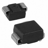
DO-214AA (SMB)
PRIMARY CHARACTERISTICS
VBR PPPM PD IFSM (uni-directional only) TJ max. 6.8 V to 220 V 600 W 5.0 W 100 A 150 °C
DEVICES FOR BI-DIRECTION APPLICATIONS For bi-directional devices use CA suffix (e.g. SM6T12CA). Electrical characteristics apply in both directions.
MAXIMUM RATINGS (TA = 25 °C unless otherwise noted)
PARAMETER Peak pulse power dissipation on 10/1000 µs waveform
(1)(2)
SYMBOL (Fig. 1) PPPM IPPM PD IFSM TJ, TSTG
VALUE 600 See next table 5.0 100 - 65 to +150
UNIT W A W A °C
Peak power pulse current with a 10/1000 µs waveform (1) (Fig. 3) Power dissipation on infinite heatsink TA = 50 °C Peak forward surge current 10 ms single half sine-wave uni-directional only (2) Operating junction and storage temperature range Notes: (1) Non-repetitive current pulse, per Fig. 3 and derated above TA = 25 °C per Fig. 2 (2) Mounted on 0.2 x 0.2" (5.0 x 5.0 mm) copper pads to each terminal
Document Number: 88385 Revision: 21-Oct-08
For technical questions within your region, please contact one of the following: PDD-Americas@vishay.com, PDD-Asia@vishay.com, PDD-Europe@vishay.com
www.vishay.com 1
�SM6T Series
Vishay General Semiconductor
ELECTRICAL CHARACTERISTICS (TA = 25 °C unless otherwise noted)
TYPE (1) DEVICE MARKING CODE UNI SM6T6V8A SM6T7V5A SM6T10A SM6T12A SM6T15A SM6T18A SM6T22A SM6T24A SM6T27A SM6T30A SM6T33A SM6T36A SM6T39A SM6T68A SM6T100A SM6T150A SM6T200A SM6T220A Notes: (1) For bi-directional devices add suffix “CA” (2) VBR measured after IT applied for 300 µs square wave pulse (3) For bipolar devices with VR = 10 V or under, the IT limit is doubled KE7 KK7 KT7 KX7 LG7 LM7 LT7 LV7 LX7 ME7 MG7 MK7 MM7 NG7 NV7 PK7 PR7 PR8 BI KE7 AK7 AT7 AX7 LG7 BM7 BT7 LV7 BX7 CE7 MG7 CK7 CM7 NG7 NV7 PK7 PR7 PR8 BREAKDOWN VOLTAGE VBR AT IT (2) (V) MIN. 6.45 7.13 9.50 11.4 14.3 17.1 20.9 22.8 25.7 28.5 31.4 34.2 37.1 64.6 95.0 143 190 209 MAX. 7.14 7.88 10.5 12.6 15.8 18.9 23.1 25.2 28.4 31.5 34.7 37.8 41.0 71.4 105 158 210 231 10 10 1.0 1.0 1.0 1.0 1.0 1.0 1.0 1.0 1.0 1.0 1.0 1.0 1.0 1.0 1.0 1.0 5.80 6.40 8.55 10.2 12.8 15.3 18.8 20.5 23.1 25.6 28.2 30.8 33.3 58.1 85.5 128 171 188 TEST CURRENT (mA) STAND-OFF VOLTAGE VRM (V) LEAKAGE CURRENT (3) IRM AT VRM (µA) 1000 500 10.0 5.0 1.0 1.0 1.0 1.0 1.0 1.0 1.0 1.0 1.0 1.0 1.0 1.0 1.0 1.0 CLAMPING VOLTAGE VC AT IPP 10/1000 µs (V) 10.5 11.3 14.5 16.7 21.2 25.2 30.6 33.2 37.5 41.5 45.7 49.9 53.9 92.0 137 207 274 328 (A) 57.0 53.0 41.0 36.0 28.0 24.0 20.0 18.0 16.0 14.5 13.1 12.0 11.1 6.50 4.40 2.90 2.20 2.00 CLAMPING VOLTAGE VC AT IPP 8/20 µs (V) 13.4 14.5 18.6 21.7 27.2 32.5 39.3 42.8 48.3 53.5 59.0 64.3 69.7 121 178 265 353 388 (A) 298 276 215 184 147 123 102 93 83 75 68 62 57 33 22.5 15 11.3 10.3 5.7 6.1 7.3 7.8 8.4 8.8 9.2 9.4 9.6 9.7 9.8 9.9 10.0 10.4 10.6 10.8 10.8 10.8 αT Max. 0-4/°C
THERMAL CHARACTERISTICS (TA = 25 °C unless otherwise noted)
PARAMETER Thermal resistance, junction to ambient air Thermal resistance, junction to leads Note: (1) Mounted on minimum recommended pad layout
(1)
SYMBOL RθJA RθJL
VALUE 100 20
UNIT °C/W °C/W
ORDERING INFORMATION (Example)
PREFERRED P/N SM6T10A-E3/52 SM6T10A-E3/5B SM6T10AHE3/52
(1)
UNIT WEIGHT (g) 0.096 0.096 0.096 0.096
PREFERRED PACKAGE CODE 52 5B 52 5B
BASE QUANTITY 750 3200 750 3200
DELIVERY MODE 7" diameter plastic tape and reel 13" diameter plastic tape and reel 7" diameter plastic tape and reel 13" diameter plastic tape and reel
SM6T10AHE3/5B (1) Note:
(1) Automotive grade AEC Q101 qualified www.vishay.com 2 For technical questions within your region, please contact one of the following: PDD-Americas@vishay.com, PDD-Asia@vishay.com, PDD-Europe@vishay.com Document Number: 88385 Revision: 21-Oct-08
�SM6T Series
Vishay General Semiconductor
RATINGS AND CHARACTERISTICS CURVES (TA = 25 °C unless otherwise noted)
100 6000 Measured at Zero Bias
PPPM - Peak Pulse Power (kW)
CJ - Junction Capacitance (pF)
1000
10
1 0.2 x 0.2" (5.0 x 5.0 mm) Copper Pad Areas 0.1 0.1 µs
100
VR, Measured at Stand-Off Voltage VWM Uni-Directional Bi-Directional TJ = 25 °C f = 1.0 MHz Vsig = 50 mVp-p 100 200
10 1.0 µs 10 µs 100 µs 1.0 ms 10 ms 1 10
td - Pulse Width (s)
VWM - Reverse Stand-Off Voltage (V)
Figure 1. Peak Pulse Power Rating Curve
Figure 4. Typical Junction Capacitance
Peak Pulse Power (PPP) or Current (IPP) Derating in Percentage, %
100
100
75
Transient Thermal Impedance (°C/W)
10
50
1.0
25
0 0 25 50 75 100 125 150 175 200
0.1 0.001
0.01
0.1
1
10
100
1000
TJ - Initial Temperature (°C)
t - Pulse Duration (s)
Figure 2. Pulse Power or Current vs. Initial Junction Temperature
Figure 5. Typical Transient Thermal Impedance
150
IPPM - Peak Pulse Current, % IRSM
Peak Forward Surge Current (A)
tr = 10 µs Peak Value IPPM
TJ = 25 °C Pulse Width (td) is defined as the Point where the Peak Current decays to 50 % of IPPM
200 8.3 ms Single Half Sine-Wave Uni-Directional Only 100
100
Half Value - IPP IPPM 2 50 10/1000 µs Waveform as defined by R.E.A. td 0 0 1.0 2.0 3.0 4.0
10 1 10 100
t - Time (ms)
Number of Cycles at 60 Hz
Figure 3. Pulse Waveform
Figure 6. Maximum Non-Repetitive Peak Forward Surge Current
Document Number: 88385 Revision: 21-Oct-08
For technical questions within your region, please contact one of the following: PDD-Americas@vishay.com, PDD-Asia@vishay.com, PDD-Europe@vishay.com
www.vishay.com 3
�SM6T Series
Vishay General Semiconductor
PACKAGE OUTLINE DIMENSIONS in inches (millimeters)
DO-214AA (SMB)
Cathode Band
0.085 (2.159) MAX.
Mounting Pad Layout
0.086 (2.20) 0.077 (1.95)
0.155 (3.94) 0.130 (3.30) 0.086 (2.18) MIN.
0.180 (4.57) 0.160 (4.06) 0.012 (0.305) 0.006 (0.152) 0.060 (1.52) MIN. 0.220 REF. 0.096 (2.44) 0.084 (2.13)
0.060 (1.52) 0.030 (0.76)
0.008 (0.2) 0 (0) 0.220 (5.59) 0.205 (5.21)
www.vishay.com 4
For technical questions within your region, please contact one of the following: PDD-Americas@vishay.com, PDD-Asia@vishay.com, PDD-Europe@vishay.com
Document Number: 88385 Revision: 21-Oct-08
�Legal Disclaimer Notice
Vishay
Disclaimer
All product specifications and data are subject to change without notice. Vishay Intertechnology, Inc., its affiliates, agents, and employees, and all persons acting on its or their behalf (collectively, “Vishay”), disclaim any and all liability for any errors, inaccuracies or incompleteness contained herein or in any other disclosure relating to any product. Vishay disclaims any and all liability arising out of the use or application of any product described herein or of any information provided herein to the maximum extent permitted by law. The product specifications do not expand or otherwise modify Vishay’s terms and conditions of purchase, including but not limited to the warranty expressed therein, which apply to these products. No license, express or implied, by estoppel or otherwise, to any intellectual property rights is granted by this document or by any conduct of Vishay. The products shown herein are not designed for use in medical, life-saving, or life-sustaining applications unless otherwise expressly indicated. Customers using or selling Vishay products not expressly indicated for use in such applications do so entirely at their own risk and agree to fully indemnify Vishay for any damages arising or resulting from such use or sale. Please contact authorized Vishay personnel to obtain written terms and conditions regarding products designed for such applications. Product names and markings noted herein may be trademarks of their respective owners.
Document Number: 91000 Revision: 18-Jul-08
www.vishay.com 1
�