T..RIA Series
Vishay High Power Products
Medium Power Phase Control Thyristors (Power Modules), 50 A/70 A/90 A
FEATURES
• • • • • • • • • Electrically isolated base plate Types up to 1200 VRRM 3500 VRMS isolating voltage Simplified mechanical designs, rapid assembly High surge capability Large creepage distances UL E78996 approved RoHS compliant Designed and qualified for industrial level
RoHS
COMPLIANT
D-55
DESCRIPTION PRODUCT SUMMARY
IT(AV) 50 A/70 A/90 A
These series of T-modules are intended for general purpose applications such as battery chargers, welders and plating equipment, regulated power supplies and temperature and speed control circuits. The semiconductors are electrically isolated from the metal base, allowing common heatsinks and compact assemblies to be built.
MAJOR RATINGS AND CHARACTERISTICS
SYMBOL IT(AV) IT(RMS) ITSM I2 t I2 √ t VRRM TJ Range 50 Hz 60 Hz 50 Hz 60 Hz CHARACTERISTICS 70 °C T50RIA 50 80 1310 1370 8550 7800 85 500 T70RIA 70 110 1660 1740 13 860 12 650 138 500 100 to 1200 - 40 to 125 T90RIA 90 141 1780 1870 15 900 14 500 159 100 UNITS A A A
A2s A 2 √s V °C
ELECTRICAL SPECIFICATIONS VOLTAGE RATINGS
TYPE NUMBER VOLTAGE CODE 10 20 T50RIA T70RIA T90RIA 40 60 80 100 120 VRRM/VDRM, MAXIMUM REPETITIVE PEAK REVERSE AND PEAK OFF-STATE VOLTAGE V 100 200 400 600 800 1000 1200 VRSM, MAXIMUM NON-REPETITIVE PEAK REVERSE VOLTAGE V 150 300 500 700 900 1100 1300 100 IRRM/IDRM MAXIMUM AT TJ = 25 °C µA
Document Number: 93756 Revision: 03-Jun-08
For technical questions, contact: ind-modules@vishay.com
www.vishay.com 1
�T..RIA Series
Vishay High Power Products Medium Power Phase Control Thyristors
(Power Modules), 50 A/70 A/90 A
ON-STATE CONDUCTION
PARAMETER Maximum average on-state current at case temperature Maximum RMS on-state current SYMBOL IT(AV) IT(RMS) t = 10 ms Maximum peak, one-cycle on-state, non-repetitive surge current t = 8.3 ms ITSM t = 10 ms t = 8.3 ms t = 10 ms Maximum I2t for fusing I2 t t = 8.3 ms t = 10 ms t = 8.3 ms Maximum I2√t for fusing I2√t VT(TO)1 VT(TO)2 rt1 rt2 VTM VFM IH IL No voltage reapplied 100 % VRRM reapplied No voltage reapplied 100 % VRRM reapplied TEST CONDITIONS 180° conduction, half sine wave 70 80 1310 1370 1100 Sine half wave, initial TJ = TJ maximum 1150 8550 7800 6050 5520 70 110 1660 1740 1400 1460 13 860 12 650 9800 8950 70 141 1780 1870 A 1500 1570 15 900 14 500 11 250 10 270 A 2 √s A2 s °C A T50RIA T70RIA T90RIA UNITS 50 70 90 A
t = 0.1 to 10 ms, no voltage reapplied (16.7 % x π x IT(AV) < I < π x IT(AV)), TJ maximum (I > π x IT(AV)), TJ maximum (16.7 % x π x IT(AV) < I < π x IT(AV)), TJ maximum (I > π x IT(AV)), TJ maximum ITM = π x IT(AV), TJ = 25 °C, tp = 400 µs square Average power = VT(TO) x IT(AV) + rf x (IT(RMS))2 ITM = π x IT(AV), TJ = 25 °C, tp = 400 µs square Average power = VT(TO) x IT(AV) + rf x (IT(RMS))2 Anode supply = 6 V, initial IT = 30 A, TJ = 25 °C Anode supply = 6 V, resistive load = 10 Ω Gate pulse: 10 V, 100 µs, TJ = 25 °C
85 500 138 500 159 100 0.97 1.13 4.1 3.3 1.60 1.60 200 400 0.77 0.88 3.6 3.2 1.55 1.55 200 400 0.78
Low level value of threshold voltage High level value of threshold voltage Low level value of on-state slope resistance High level value of on-state slope resistance Maximum on-state voltage drop Maximum forward voltage drop Maximum holding current Maximum latching current
V 0.88 2.9 mΩ 2.6 1.55 1.55 200 mA 400 V V
SWITCHING
PARAMETER Typical turn-on time Typical reverse recovery time Typical turn-off time SYMBOL tgd trr tq TEST CONDITIONS TJ = 25 °C, Vd = 50 % VDRM, ITM = 50 A Ig = 500 mA, tr ≤ 0.5, tp ≥ 6 µs TJ = 125 °C, ITM = 50 A, tp = 300 µs, dI/dt = 10 A/µs TJ = TJ maximum, ITM = 50 A, tp = 300 µs -dI/dt = 15 A/µs, VR = 100 V, linear to 80 % VDRM VALUES 0.9 3 110 µs UNITS
www.vishay.com 2
For technical questions, contact: ind-modules@vishay.com
Document Number: 93756 Revision: 03-Jun-08
�T..RIA Series
Medium Power Phase Control Thyristors Vishay High Power Products (Power Modules), 50 A/70 A/90 A
BLOCKING
PARAMETER Maximum peak reverse and off-state leakage current RMS isolation voltage Critical rate of rise of off-state voltage SYMBOL IRRM, IDRM VISOL dV/dt TJ = TJ maximum 50 Hz, circuit to base, all terminals shorted, TJ = 25 °C, t = 1 s TJ = TJ maximum, linear to 80 % rated VDRM (1) TEST CONDITIONS VALUES 15 3500 500 UNITS mA V V/µs
Note (1) Available with dV/dt = 1000 V/µs, to complete code add S90 i.e. T90RIA80S90
TRIGGERING
PARAMETER Maximum peak gate power Maximum average gate power Maximum peak gate current Maximum peak negative gate voltage Maximum required DC gate voltage to trigger SYMBOL PGM PG(AV) IGM -VGT TJ = TJ maximum, tp ≤ 5 ms TJ = - 40 °C VGT TJ = 25 °C TJ = TJ maximum TJ = - 40 °C Maximum required DC gate current to trigger Maximum gate voltage that will not trigger Maximum gate current that will not trigger IGT TJ = 25 °C TJ = TJ maximum VGD TJ = TJ maximum, rated VDRM applied IGD VD = 0.67 rated VDRM, ITM = 2 x rated dI/dt Ig = 400 mA for T50RIA and Ig = 500 mA for T70RIA/T90RIA; tr < 0.5 µs, tp ≥ 6 µs For repetitive value use 40 % non-repetitive Per JEDEC STD. RS397, 5.2.2.6 5.0 200 180 160 150 6.0 200 180 160 150 6.0 200 180 A/µs 160 150 mA Anode supply = 6 V, resistive load; Ra = 1 Ω TEST CONDITIONS TJ = TJ maximum, tp ≤ 5 ms TJ = TJ maximum, f = 50 Hz T50RIA T70RIA T90RIA UNITS 10 2.5 2.5 10 4.0 2.5 1.5 250 100 50 0.2 12 3 3 10 4.0 2.5 1.5 270 120 60 0.2 12 W 3 3 10 4.0 2.5 1.5 270 120 60 0.2 V mA V A V
Maximum rate of rise of turned-on current
dI/dt
Document Number: 93756 Revision: 03-Jun-08
For technical questions, contact: ind-modules@vishay.com
www.vishay.com 3
�T..RIA Series
Vishay High Power Products Medium Power Phase Control Thyristors
(Power Modules), 50 A/70 A/90 A
THERMAL AND MECHANICAL SPECIFICATIONS
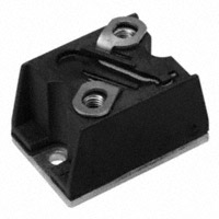
PARAMETER Maximum junction operating temperature range Maximum storage temperature range Maximum thermal resistance, junction to case per junction Maximum thermal resistance, case to heatsink to heatsink Mounting torque, ± 10 % terminals Approximate weight Case style T-module SYMBOL TJ TStg RthJC RthCS DC operation Mounting surface, smooth, flat and greased Non-lubricated threads M3.5 mounting screws (1) M5 screw terminals 0.65 TEST CONDITIONS T50RIA T70RIA T90RIA UNITS - 40 to 125 °C - 40 to 150 0.50 0.2 1.3 ± 10 % Nm 3 ± 10 % 54 D-55 g 0.38 K/W
Note (1) A mounting compund is recommended and the torque should be rechecked after a period of 3 hours to allow for the spread of the compound
ΔR CONDUCTION PER JUNCTION
DEVICES T50RIA T70RIA T90RIA SINUSOIDAL CONDUCTION AT TJ MAXIMUM 180° 0.08 0.07 0.05 120° 0.10 0.08 0.06 90° 0.13 0.10 0.08 60° 0.19 0.14 0.12 30° 0.31 0.24 0.20 RECTANGULAR CONDUCTION AT TJ MAXIMUM 180° 0.06 0.05 0.04 120° 0.10 0.08 0.06 90° 0.14 0.11 0.09 60° 0.20 0.15 0.12 30° 0.32 0.24 0.20 K/W UNITS
Note • Table shows the increment of thermal resistance RthJC when devices operate at different conduction angles than DC
www.vishay.com 4
For technical questions, contact: ind-modules@vishay.com
Document Number: 93756 Revision: 03-Jun-08
�T..RIA Series
Medium Power Phase Control Thyristors Vishay High Power Products (Power Modules), 50 A/70 A/90 A
Maximum Allowable Case Temperature (°C) Maximum Allowable Case Temperature (°C) 130 120 110 100 90 80 70 60 50 0 10 20 30 40 50 60 Average On-state Current (A) 30° 60° 90° 120° 180°
Conduction Angle
T50RIA.. Series R thJC (DC) = 0.65 K/W
130 120 110 100 90 80 70
T50RIA.. Series R thJC (DC) = 0.65 K/W
Conduction Period
60° 60 50 0 10 20 30 30°
90° 120° 180° 40 50 60 DC 70 80
Average On-state Current (A)
Fig. 1 - Current Ratings Characteristics
Fig. 2 - Current Ratings Characteristics
Maximum Average On-state Power Loss (W)
80
K/W 0.3 K/W 0.5
70 60 50
180° 120° 90° 60° 30° RMS Limit
R th
0. 7
K/ W
SA
K/W .1 =0
1
K/ W
1.5 K/W
2K /W
a elt -D R
40 30
Conduction Angle
3K /W
5 K/W
20 10 0 0 10 20 30 40 T50RIA.. Series TJ= 125°C
10 K/W
0 50
20
40
60
80
100
120
Average On-state Current (A)
Maximum Allowable Ambient Temperature (°C)
Fig. 3 - On-State Power Loss Characteristics
Maximum Average On-state Power Loss (W)
110 100 90 80 70 60 50 RMS Limit 40 30 20 10 0 0 10 20 30 40 50 60 70 80 0 20 40 60 80 100 120 Average On-state Current (A) Maximum Allowable Ambient Temperature (°C)
Conduction Period
DC 180° 120° 90° 60° 30°
R th
0. 5 K/ W 0.7 K/ W 1K /W
1.5 K/W 2K /W
3 K/ W
T50RIA.. Series TJ = 125°C
5 K/W
Fig. 4 - On-State Power Loss Characteristics
/W 3K 0.
SA
W K/ .1 =0 ta el -D R
Document Number: 93756 Revision: 03-Jun-08
For technical questions, contact: ind-modules@vishay.com
www.vishay.com 5
�T..RIA Series
Vishay High Power Products Medium Power Phase Control Thyristors
(Power Modules), 50 A/70 A/90 A
1200 Peak Half Sine Wave On-state Current (A) 1100 1000 900 800 700 600 500 1 10 100
Number Of Equal Amplitude Half Cycle Current Pulses (N)
Peak Half Sine Wave On-state Current (A)
At Any Rated Load Condition And With Rated V RRM Applied Following Surge.
1300 1200 1100 1000 900 800 700 600
Initial TJ = 125°C @ 60 Hz 0.0083 s @ 50 Hz 0.0100 s
Maximum Non Repetitive Surge Current Versus Pulse Train Duration. Control Of Conduction May Not Be Maintained. Initial TJ= 125°C No Voltage Reapplied Rated V RRM Reapplied
T50RIA.. Series
T50RIA.. Series
500 0.01
0.1 Pulse Train Duration (s)
1
Fig. 5 - Maximum Non-Repetitive Surge Current
Fig. 6 - Maximum Non-Repetitive Surge Current
1000 Instantaneous On-state Current (A)
100
TJ= 25°C 10 TJ = 125°C
T50RIA.. Series 1 0.5 1 1.5 2 2.5 3 3.5 4 4.5
Instantaneous On-state Voltage (V)
Fig. 7 - On-State Voltage Drop Characteristics
100 Instantaneous Gate Voltage (V)
Rectangular gate pulse a) Recommended load line for rated di/dt : 20V, 30ohms; tr=0.5µs, tp>=6µs b) Recommended load line for =6µs (b)
Tj=-40 °C Tj=25 °C
(1) PGM = 10W, tp = 5ms (2) PGM = 20W, tp = 2ms (3) PGM = 50W, tp = 1ms (4) PGM = 100W, tp = 500µs
(a)
Tj=125 °C
1
(1) (2)
(3) (4)
VGD IGD 0.1 0.001 0.01 0.1 T50RIA.. Series 1 Frequency Limited by PG(AV) 10 100 1000
Instantaneous Gate Current (A)
Fig. 8 - Gate Characteristics
www.vishay.com 6
For technical questions, contact: ind-modules@vishay.com
Document Number: 93756 Revision: 03-Jun-08
�T..RIA Series
Medium Power Phase Control Thyristors Vishay High Power Products (Power Modules), 50 A/70 A/90 A
Maximum Allowable Case Temperature (°C)
120 110 100 90 80 70 60 50 0 10
T70RIA.. Series R thJC (DC) = 0.50 K/W
Maximum Allowable Case Temperature (°C)
130
130 120 110 100
T70RIA.. Series RthJC (DC) = 0.50 K/W
Conduction Angle
Conduction Period
90 80 70 60 50 0 20 40 60 80 100 120 Average On-state Current (A) 60° 30° 90° 120° 180° DC
30°
60° 90° 120° 180° 70 80
20
30
40
50
60
Average On-state Current (A)
Fig. 9 - Current Ratings Characteristics
Fig. 10 - Current Ratings Characteristics
Maximum Average On-state Power Loss (W)
100 90 80 70 60 50 40 30 20 10 0 0 10 20 30 40 50 60 70 0 20 40 60 80 100 120 Average On-state Current (A) Maximum Allowable Ambient Temperature (°C)
Conduction Angle
180° 120° 90° 60° 30° RMS Limit
/W 3K 0.
R thS
0.7
0. 5
K/ W
K/ W
A
K/W .1 =0
1K /W
1.5 K/W 2K /W
aR elt -D
3K /W
5 K/W
T70RIA.. Series TJ = 125°C
7 K/W
Fig. 11 - On-State Power Loss Characteristics
Maximum Average On-state Power Loss (W)
140 120 100 80 RMS Limit 60 40 20 0 0 20 40 60 80 100 0 120 20 40 60 80 100 120 Average On-state Current (A) Maximum Allowable Ambient Temperature (°C)
Conduction Period
DC 180° 120° 90° 60° 30°
R
0. 3 K/ W 0.5 K/ W 0.7 K/W 1K /W
1.5 K/W
2K /W
3 K/W
5 K/W
A thS
= 1 0. W K/ ta el -D R
T70RIA.. Series TJ = 125°C
Fig. 12 - On-State Power Loss Characteristics
Document Number: 93756 Revision: 03-Jun-08
For technical questions, contact: ind-modules@vishay.com
www.vishay.com 7
�T..RIA Series
Vishay High Power Products Medium Power Phase Control Thyristors
(Power Modules), 50 A/70 A/90 A
1500 Peak Half Sine Wave On-state Current (A) 1400 1300 1200 1100 1000 900 800 700 1 10 100
Number Of Equal Amplitude Half Cycle Current Pulses (N)
Peak Half Sine Wave On-state Current (A)
At Any Rated Load Condition And With Rated V RRM Applied Following Surge. Initial TJ = 125°C @ 60 Hz 0.0083 s @ 50 Hz 0.0100 s
1700 1600 1500 1400 1300 1200 1100 1000 900 800 700
Maximum Non Repetitive Surge Current Versus Pulse Train Duration. Control Of Conduction May Not Be Maintained. Initial T = 125°C J No Voltage Reapplied Rated VRRM Reapplied
T70RIA.. Series
T70RIA.. Series
600 0.01
0.1 Pulse Train Duration (s)
1
Fig. 13 - Maximum Non-Repetitive Surge Current
Fig. 14 - Maximum Non-Repetitive Surge Current
1000 Instantaneous On-state Current (A)
100
TJ= 25°C 10 TJ= 125°C
T70RIA.. Series 1 0 0.5 1 1.5 2 2.5 3 3.5 4 Instantaneous On-state Voltage (V)
Fig. 15 - On-State Voltage Drop Characteristics
100 Instantaneous Gate Voltage (V)
Rectangular gate pulse a) Recommended load line for rated di/dt : 20V, 20ohms; tr=0.5µs, tp>=6µs b) Recommended load line for =6µs (b)
Tj=-40 °C Tj=25 °C
(1) PGM = 12W, tp = 5ms (2) PGM = 30W, tp = 2ms (3) PGM = 60W, tp = 1ms (4) PGM = 200W, tp = 300µs
(a)
Tj=125 °C
1
(1)
(2) (3)
(4)
VGD 0.1 0.001 IGD 0.01 T70RIA.., T90RIA.. Series Frequency Limited by PG(AV) 0.1 1 10 100 1000
Instantaneous Gate Current (A)
Fig. 16 - Gate Characteristics
www.vishay.com 8
For technical questions, contact: ind-modules@vishay.com
Document Number: 93756 Revision: 03-Jun-08
�T..RIA Series
Medium Power Phase Control Thyristors Vishay High Power Products (Power Modules), 50 A/70 A/90 A
Maximum Allowable Case Temperature (°C) T90RIA.. Series R thJC (DC) = 0.38 K/W
Maximum Allowable Case Temperature (°C)
130 120 110 100 90 80 70 60 50 0 20
130 120 110 100 90 80 70 60 50 0 20
T90RIA.. Series R thJC (DC) = 0.38 K/W
Conduction Angle
Conduction Period
30°
60°
90°
90° 60° 30° 40 60 120° 180° DC
120°
180° 100
40
60
80
80 100 120 140 160
Average On-state Current (A)
Average On-state Current (A)
Fig. 17 - Current Ratings Characteristics
Fig. 18 - Current Ratings Characteristics
Maximum Average On-state Power Loss (W)
140 120 100 80 60 40 20 0 0 10 20 30 40 50 60 70 80 0 90 20 40 60 80 100 120 Average On-state Current (A) Maximum Allowable Ambient Temperature (°C)
Conduction Angle
180° 120° 90° 60° 30° RMS Limit
R th
0. 3
0. 5K /W 0.7 K/W
SA
K/ W
= /W 1K 0. a elt -D
1K /W
1.5 K/W
R
2 K/W
3 K/W
T90RIA Series TJ = 125°C
Fig. 19 - On-State Power Loss Characteristics
Maximum Average On-state Power Loss (W)
180 160 140 120 100 80 RMS Limit 60 40 20 0 0 20 40 60 80 100 120 140 160 0 20 40 60 80 100 120 Average On-state Current (A) Maximum Allowable Ambient Temperature (°C) T90RIA.. Series TJ = 125°C
Conduction Period
DC 180° 120° 90° 60° 30°
0. 3K /W
0. 5K /W
R
A thS
= 1 0. W K/ ta el -D R
0.7
K/W 1K /W
1.5 K/W
2 K/ W
Fig. 20 - On-State Power Loss Characteristics
Document Number: 93756 Revision: 03-Jun-08
For technical questions, contact: ind-modules@vishay.com
www.vishay.com 9
�T..RIA Series
Vishay High Power Products Medium Power Phase Control Thyristors
(Power Modules), 50 A/70 A/90 A
1600 Peak Half Sine Wave On-state Current (A) 1500 1400 1300 1200 1100 1000 900 800 700 1 10 100
Number Of Equal Amplitude Half Cycle Current Pulses (N)
Peak Half Sine Wave On-state Current (A)
At Any Rated Load Condition And With Rated V RRM Applied Following Surge. Initial TJ = 125°C @ 60 Hz 0.0083 s @ 50 Hz 0.0100 s
1800 1700 1600 1500 1400 1300 1200 1100 1000 900 800
Maximum Non Repetitive Surge Current Versus Pulse Train Duration. Control Of Conduction May Not Be Maintained. Initial TJ = 125°C No Voltage Reapplied Rated V RRMReapplied
T90RIA.. Series
T90RIA.. Series
700 0.01
0.1 Pulse Train Duration (s)
1
Fig. 21 - Maximum Non-Repetitive Surge Current
Fig. 22 - Maximum Non-Repetitive Surge Current
1000 Instantaneous On-state Current (A)
100
TJ = 25°C 10 TJ = 125°C
T90RIA.. Series 1 0 0.5 1 1.5 2 2.5 3 3.5 Instantaneous On-state Voltage (V)
Fig. 23 - On-State Voltage Drop Characteristics
Transient Thermal Impedance Z thJC (K/W)
1 Steady State Value R thJC = 0.65 K/W R thJC = 0.50 K/W R thJC = 0.38 K/W (DC Operation) 0.1 T50RIA.. Series T70RIA.. Series T90RIA.. Series
0.01 0.001
0.01
0.1
1
10
100
Square Wave Pulse Duration (s)
Fig. 24 - Thermal Impedance ZthJC Characteristics
www.vishay.com 10
For technical questions, contact: ind-modules@vishay.com
Document Number: 93756 Revision: 03-Jun-08
�T..RIA Series
Medium Power Phase Control Thyristors Vishay High Power Products (Power Modules), 50 A/70 A/90 A
ORDERING INFORMATION TABLE
Device code
T
1
1 2 3 4
50
2 -
RIA
3
120
4
Module type Current rating Circuit configuration Voltage code x 10 = VRRM
CIRCUIT CONFIGURATION
+
G
-
LINKS TO RELATED DOCUMENTS Dimensions http://www.vishay.com/doc?95336
Document Number: 93756 Revision: 03-Jun-08
For technical questions, contact: ind-modules@vishay.com
www.vishay.com 11
�Legal Disclaimer Notice
Vishay
Disclaimer
All product specifications and data are subject to change without notice. Vishay Intertechnology, Inc., its affiliates, agents, and employees, and all persons acting on its or their behalf (collectively, “Vishay”), disclaim any and all liability for any errors, inaccuracies or incompleteness contained herein or in any other disclosure relating to any product. Vishay disclaims any and all liability arising out of the use or application of any product described herein or of any information provided herein to the maximum extent permitted by law. The product specifications do not expand or otherwise modify Vishay’s terms and conditions of purchase, including but not limited to the warranty expressed therein, which apply to these products. No license, express or implied, by estoppel or otherwise, to any intellectual property rights is granted by this document or by any conduct of Vishay. The products shown herein are not designed for use in medical, life-saving, or life-sustaining applications unless otherwise expressly indicated. Customers using or selling Vishay products not expressly indicated for use in such applications do so entirely at their own risk and agree to fully indemnify Vishay for any damages arising or resulting from such use or sale. Please contact authorized Vishay personnel to obtain written terms and conditions regarding products designed for such applications. Product names and markings noted herein may be trademarks of their respective owners.
Document Number: 91000 Revision: 18-Jul-08
www.vishay.com 1
�