VO615A
Vishay Semiconductors
Optocoupler, Phototransistor Output, High Temperature, 110 °C, Rated
FEATURES
• CTR offered in 9 groups • Isolation materials according to UL94-VO • Pollution degree 2 (DIN/VDE 0110/resp. IEC 60664)
C E
• Climatic classification 40/110/21 (IEC 60068 part 1) • Temperature range - 40 °C to + 110 °C
V DE
17918_2
1
C
C
• Rated impulse VIOTM = 8 kVpeak
voltage
(transient
overvoltage)
A
• Isolation test voltage (partial discharge test voltage) Vpd = 1.6 kV • Rated isolation VIOWM = 600 VRMS • Rated recurring VIORM = 850 Vpeak voltage peak (RMS includes DC)
DESCRIPTION
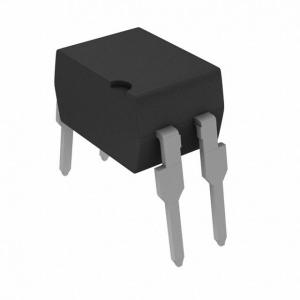
The VO615A consists of a phototransistor optically coupled to a gallium arsenide infrared-emitting diode in a 4-pin plastic dual inline package. The elements are mounted on one leadframe, providing a fixed distance between input and output for highest safety requirements.
voltage
(repetitive)
• Creepage current resistance according to VDE 0303/ IEC 60112 comparative tracking index: CTI ≥ 175 • Thickness through insulation ≥ 0.75 mm • External creepage distance > 8 mm
APPLICATIONS
Circuits for safe protective separation against electrical shock according to safety class II (reinforced isolation): • for appl. class I - IV at mains voltage ≤ 300 V • for appl. class I - IV at mains voltage ≤ 600 V according to table 1 of IEC 60664-1, suitable for: - Switch-mode power supplies - Line receiver - Computer peripheral interface - Microprocessor system interface
AGENCY APPROVALS
• BSI: EN 60065:2002, 8967/8968 EN 60950:2000 certificate
• DIN EN 60747-5-2 (VDE 0884) pending DIN EN 60747-5-5 pending • FIMKO pending
ORDER INFORMATION
PART VO615A VO615A-1 VO615A-2 VO615A-3 VO615A-4 VO615A-5 VO615A-6 VO615A-7 VO615A-8 VO615A-9 VO615A-X006 VO615A-1X006 VO615A-2X006 VO615A-3X006 VO615A-4X006 VO615A-5X006 Document Number: 81753 Rev. 1.0, 04-Mar-08 REMARKS CTR 50 to 600 %, DIP-4 CTR 40 to 80 %, DIP-4 CTR 63 to 125 %, DIP-4 CTR 100 to 200 %, DIP-4 CTR 160 to 320 %, DIP-4 CTR 50 to 150 %, DIP-4 CTR 100 to 300 %, DIP-4 CTR 80 to 160 %, DIP-4 CTR 130 to 260 %, DIP-4 CTR 200 to 400 %, DIP-4 CTR 50 to 600 %, DIP-4, 400 mil (option 6) CTR 40 to 80 %, DIP-4, 400 mil (option 6) CTR 63 to 125 %, DIP-4, 400 mil (option 6) CTR 100 to 200 %, DIP-4, 400 mil (option 6) CTR 160 to 320 %, DIP-4, 400 mil (option 6) CTR 50 to 150 %, DIP-4, 400 mil (option 6) For technical questions, contact: optocoupler.answers@vishay.com www.vishay.com 1
�VO615A
Vishay Semiconductors Optocoupler, Phototransistor Output,
High Temperature, 110 °C, Rated
ORDER INFORMATION
PART VO615A-6X006 VO615A-7X006 VO615A-8X006 VO615A-9X006 VO615A-X007 VO615A-1X007 VO615A-2X007 VO615A-3X007 VO615A-4X007 VO615A-5X007 VO615A-6X007 VO615A-7X007 VO615A-8X007 VO615A-9X007 VO615A-X009 VO615A-1X009 VO615A-2X009 VO615A-3X009 VO615A-4X009 REMARKS CTR 100 to 300 %, DIP-4, 400 mil (option 6) CTR 80 to 160 %, DIP-4, 400 mil (option 6) CTR 130 to 260 %, DIP-4, 400 mil (option 6) CTR 200 to 400 %, DIP-4, 400 mil (option 6) CTR 50 to 600 %, SMD-4 (option 7) CTR 40 to 80 %, SMD-4 (option 7) CTR 63 to 125 %, SMD-4 (option 7) CTR 100 to 200 %, SMD-4 (option 7) CTR 160 to 320 %, SMD-4 (option 7) CTR 50 to 150 %, SMD-4 (option 7) CTR 100 to 300 %, SMD-4 (option 7) CTR 80 to 160 %, SMD-4 (option 7) CTR 130 to 260 %, SMD-4 (option 7) CTR 200 to 400 %, SMD-4 (option 7) CTR 50 to 600 %, SMD-4 (option 9) CTR 40 to 80 %, SMD-4 (option 9) CTR 63 to 125 %, SMD-4 (option 9) CTR 100 to 200 %, SMD-4 (option 9) CTR 160 to 320 %, SMD-4 (option 9)
Note For additional information on the possible lead bend and VDE options refer to option information.
ABSOLUTE MAXIMUM RATINGS (1)
PARAMETER INPUT Reverse voltage Forward current Forward surge current LED power dissipation OUTPUT Collector emitter voltage Emitter collector voltage Collector current Collector peak current Output power dissipation COUPLER Isolation test voltage (RMS) Operating ambient temperature range Storage temperature range Soldering temperature (2) 2 mm from case, ≤ 10 s t = 1 min VISO Tamb Tstg Tsld 5000 - 40 to + 110 - 40 to + 125 260 VRMS °C °C °C tP/T = 0.5, tP ≤ 10 ms at 25 °C VCEO VECO IC ICM Pdiss 70 7 50 100 150 V V mA mA mW tP ≤ 10 µs at 25 °C VR IF IFSM Pdiss 6 60 1.5 100 V mA A mW TEST CONDITION SYMBOL VALUE UNIT
Notes (1) T amb = 25 °C, unless otherwise specified. Stresses in excess of the absolute maximum ratings can cause permanent damage to the device. Functional operation of the device is not implied at these or any other conditions in excess of those given in the operational sections of this document. Exposure to absolute maximum ratings for extended periods of the time can adversely affect reliability. (2) Refer to reflow profile for soldering conditions for surface mounted devices (SMD). Refer to wave profile for soldering conditions for through hole devices (DIP).
www.vishay.com 2
For technical questions, contact: optocoupler.answers@vishay.com
Document Number: 81753 Rev. 1.0, 04-Mar-08
�VO615A
Optocoupler, Phototransistor Output, Vishay Semiconductors High Temperature, 110 °C, Rated
THERMAL CHARACTERISTICS
PARAMETER Maximum LED junction temperature Maximum output die junction temperature Thermal resistance, junction emitter to board Thermal resistance, junction emitter to case Thermal resistance, junction detector to board Thermal resistance, junction detector to case Thermal resistance, junction emitter to junction detector Thermal resistance, board to ambient (2) Thermal resistance, case to ambient (2)
(1)
TEST CONDITION
SYMBOL Tjmax Tjmax θEB θEC θDB θDC θED θBA θCA
VALUE 125 125 173 149 111 127 173 197 4041
UNIT °C °C °C/W °C/W °C/W °C/W °C/W °C/W °C/W
Notes (1) The thermal model is represented in the thermal network below. Each resistance value given in this model can be used to calculate the temperatures at each node for a given operating condition. The thermal resistance from board to ambient will be dependent on the type of PCB, layout and thickness of copper traces. For a detailed explanation of the thermal model, please reference Vishay's Thermal Characteristics of Optocouplers Application note. (2) For 2 layer FR4 board (4" x 3" x 0.062).
TA
θCA
TC Package
θDC
TJD
θEC θDE
TJE
θDB
TB
θEB
θBA
19996
TA
Document Number: 81753 Rev. 1.0, 04-Mar-08
For technical questions, contact: optocoupler.answers@vishay.com
www.vishay.com 3
�VO615A
Vishay Semiconductors Optocoupler, Phototransistor Output,
High Temperature, 110 °C, Rated
ELECTRICAL CHARACTERISTICS (1)
PARAMETER INPUT Forward voltage Junction capacitance OUTPUT Collector emitter voltage Emitter collector voltage Collector emitter cut-off current COUPLER Collector emitter saturation voltage Cut-off frequency Coupling capacitance IF = 10 mA, IC = 1 mA VCE = 5 V, IF = 10 mA, RL = 100 Ω f = 1 MHz VCEsat fc Ck 110 0.3 0.3 V kHz pF I C = 1 mA IE = 100 µA VCE = 20 V, If = 0, E = 0 VCEO VECO ICEO 70 7 10 100 V V nA IF = ± 50 mA VR = 0, f = 1 MHz VF Cj 1.25 50 1.6 V pF TEST CONDITION SYMBOL MIN. TYP. MAX. UNIT
Note Tamb = 25 °C, unless otherwise specified. Minimum and maximum values are testing requirements. Typical values are characteristics of the device and are the result of engineering evaluation. Typical values are for information only and are not part of the testing requirements.
CURRENT TRANSFER RATIO
PARAMETER TEST CONDITION PART VO615A-1 VCE = 5 V, IF = 1 mA VO615A-2 VO615A-3 VO615A-4 VO615A VO615A-5 IC/IF VCE = 5 V, IF = 5 mA VO615A-6 VO615A-7 VO615A-8 VO615A-9 VO615A-1 VCE = 5 V, IF = 10 mA VO615A-2 VO615A-3 VO615A-4 SYMBOL CTR CTR CTR CTR CTR CTR CTR CTR CTR CTR CTR CTR CTR CTR MIN. 13 22 34 56 50 50 100 80 130 200 40 63 100 160 TYP. 30 45 70 90 600 150 300 160 260 400 80 125 200 320 MAX. UNIT % % % % % % % % % % % % % %
www.vishay.com 4
For technical questions, contact: optocoupler.answers@vishay.com
Document Number: 81753 Rev. 1.0, 04-Mar-08
�VO615A
Optocoupler, Phototransistor Output, Vishay Semiconductors High Temperature, 110 °C, Rated
MAXIMUM SAFETY RATINGS
PARAMETER INPUT Forward current OUTPUT Power dissipation COUPLER Safety temperature Tsi 150 °C Note According to DIN EN 60747-5-2 (VDE 0884)/DIN EN 60747-5-5 pending (see figure 1). This optocoupler is suitable for safe electrical isolation only within the safety ratings. Compliance with the safety ratings shall be ensured by means of suitable protective circuits. Pdiss 265 mW IF 130 mA TEST CONDITION SYMBOL MIN. TYP. MAX. UNIT
INSULATION RATED PARAMETERS
PARAMETER Partial discharge test voltage routine test Partial discharge test voltage lot test (sample test) TEST CONDITION 100 %, ttest = 1 s tTr = 60 s, ttest = 10 s, (see figure 2) VIO = 500 V Insulation resistance VIO = 500 V, Tamb = 100 °C VIO = 500 V, Tamb = 150 °C (construction test only) Rated impulse voltage Max. working voltages Recurring peak voltage SYMBOL Vpd Vpd RIO RIO RIO VIOTM VIORM 850 MIN. 1.6 1.3 1012 1011 109 8 TYP. MAX. UNIT kV kV Ω Ω Ω kV Vpeak
Ptot - Total Power Dissipation (mW)
300 250 200 Phototransistor Psi (mW)
VIOTM t1, t2 t3 , t4 ttest tstres VPd = 1 to 10 s =1s = 10 s = 12 s
150 100 50 0 0 25 50 75 100 125 IR-Diode Isi (mA) 150
VIOWM VIORM
0
13930
t3 ttest t4 t1 tTr = 60 s t2 t stres t
94 9182
Tsi - Safety Temperature (°C)
Fig. 1 - Derating Diagram
Fig. 2 - Test Pulse Diagram for Sample Test According to DIN EN 60747-5-2 (VDE 0884)/DIN EN 60747-; IEC 60747
Document Number: 81753 Rev. 1.0, 04-Mar-08
For technical questions, contact: optocoupler.answers@vishay.com
www.vishay.com 5
�VO615A
Vishay Semiconductors Optocoupler, Phototransistor Output,
High Temperature, 110 °C, Rated
SWITCHING CHARACTERISTICS
PARAMETER Delay time Rise time Fall time Storage time Turn-on time Turn-off time Turn-on time Turn-off time TEST CONDITION VS = 5 V, IC = 2 mA, RL = 100 Ω, (see figure 3) VS = 5 V, IC = 2 mA, RL = 100 Ω, (see figure 3) VS = 5 V, IC = 2 mA, RL = 100 Ω, (see figure 3) VS = 5 V, IC = 2 mA, RL = 100 Ω, (see figure 3) VS = 5 V, IC = 2 mA, RL = 100 Ω, (see figure 3) VS = 5 V, IC = 2 mA, RL = 100 Ω, (see figure 3) VS = 5 V, IF = 10 mA, RL = 1 kΩ, (see figure 4) VS = 5 V, IF = 10 mA, RL = 1 kΩ, (see figure 4) SYMBOL td tr tf ts ton toff ton toff MIN TYP. 3.0 3.0 4.7 0.3 6.0 5.0 9.0 10.0 MAX UNIT µs µs µs µs µs µs µs µs
IF
IF 0 IF +5V IC = 2 mA; adjusted through input amplitude
0 IC 100 % 90 %
tp
t
RG = 50 tp = 0.01 T tp = 50 µs
Channel I Channel II 50 100 Oscilloscope RL = 1 M CL = 20 pF
10 % 0
tr td t on
Pulse duration Delay time Rise time Turn-on time
ts
tf t off
t
Storage time Fall time Turn-off time
95 10804
tp td tr t on (= t d + tr)
96 11698
ts tf t off (= ts + tf)
Fig. 3 - Test Circuit, Non-Saturated Operation
Fig. 5 - Switching Times
IF 0
IF = 10 mA
+5V IC
R G = 50 Ω tp = 0.01 T t p = 50 µs
Channel I Channel II 50 Ω 1 kΩ Oscilloscope R L ≥ 1 MΩ C L ≤ 20 pF
95 10843
Fig. 4 - Test Circuit, Saturated Operation
www.vishay.com 6
For technical questions, contact: optocoupler.answers@vishay.com
Document Number: 81753 Rev. 1.0, 04-Mar-08
�VO615A
Optocoupler, Phototransistor Output, Vishay Semiconductors High Temperature, 110 °C, Rated
PACKAGE DIMENSIONS in millimeters
0.268 (6.81) 0.255 (6.48)
Pin 1 Identifier
0.190 (4.83) 0.179 (4.55) 0.312 (7.92) 0.296 (7.52)
ISO Method A
0.045 (1.14) 0.030 (0.76)
0.033 (0.84) 0.029 (0.74)
0.150 (3.81) 0.130 (3.30)
0.250 (6.35) 0.230 (5.84) 0.130 (3.30) 0.110 (2.79) 3° to 9° 0.012 (0.30)
0.035 (0.89) 0.020 (0.51) 0.052 (1.32) 0.048 (1.22) 0.105 (2.67) 0.095 (2.41) 0.008 (0.20)
i178027-2
Option 6
0.407 (10.36) 0.391 (9.96) 0.307 (7.8) 0.291 (7.4) 0.028 (0.7)
Option 7
0.300 (7.62) typ.
Option 8
0.300 (7.62) typ.
0.098 (0.249) 0.040 (0.102)
0.180 (4.6) 0.160 (4.1)
Option 9
0.395 (10.03) 0.375 (9.53) 0.312 (7.92) 0.296 (7.52) 0.012 (0.30) 0.008 (0.20) 0.040 (1.02) 0.020 (0.51) 0.315 (8.00)
0.020 (0.50) 0.000 (0.00)
0.150 (3.81) 0.130 (3.30) 0.365 (9.27) min. 0.472 (12.00) max.
0.315 (8.0) min. 0.014 (0.35) 0.010 (0.25) 0.400 (10.16) 0.430 (10.92) 0.331 (8.4) min. 0.406 (10.3) max.
15° max.
min.
0.100 (2.54)
0.100 (2.54)
0.030 (0.76)
0.100 (2.54)
R 0.010 (0.25) 20802 0.060 (1.52) 0.315 (8.00) min. 0.435 (11.05)
0.030 (0.76)
R 0.010 (0.25) 0.060 (1.52) 0.392 (9.95) min. 0.512 (13.00)
R 0.010 (0.25) 0.060 (1.52) 0.315 (8.00) min. 0.435 (11.05)
0.070 (1.78)
0.070 (1.78)
Document Number: 81753 Rev. 1.0, 04-Mar-08
For technical questions, contact: optocoupler.answers@vishay.com
www.vishay.com 7
0.070 (1.78)
0.030 (0.76)
�VO615A
Vishay Semiconductors Optocoupler, Phototransistor Output,
High Temperature, 110 °C, Rated
OZONE DEPLETING SUBSTANCES POLICY STATEMENT
It is the policy of Vishay Semiconductor GmbH to 1. Meet all present and future national and international statutory requirements. 2. Regularly and continuously improve the performance of our products, processes, distribution and operating systems with respect to their impact on the health and safety of our employees and the public, as well as their impact on the environment. It is particular concern to control or eliminate releases of those substances into the atmosphere which are known as ozone depleting substances (ODSs). The Montreal Protocol (1987) and its London Amendments (1990) intend to severely restrict the use of ODSs and forbid their use within the next ten years. Various national and international initiatives are pressing for an earlier ban on these substances. Vishay Semiconductor GmbH has been able to use its policy of continuous improvements to eliminate the use of ODSs listed in the following documents. 1. Annex A, B and list of transitional substances of the Montreal Protocol and the London Amendments respectively. 2. Class I and II ozone depleting substances in the Clean Air Act Amendments of 1990 by the Environmental Protection Agency (EPA) in the USA. 3. Council Decision 88/540/EEC and 91/690/EEC Annex A, B and C (transitional substances) respectively. Vishay Semiconductor GmbH can certify that our semiconductors are not manufactured with ozone depleting substances and do not contain such substances.
We reserve the right to make changes to improve technical design and may do so without further notice. Parameters can vary in different applications. All operating parameters must be validated for each customer application by the customer. Should the buyer use Vishay Semiconductors products for any unintended or unauthorized application, the buyer shall indemnify Vishay Semiconductors against all claims, costs, damages, and expenses, arising out of, directly or indirectly, any claim of personal damage, injury or death associated with such unintended or unauthorized use. Vishay Semiconductor GmbH, P.O.B. 3535, D-74025 Heilbronn, Germany
www.vishay.com 8
For technical questions, contact: optocoupler.answers@vishay.com
Document Number: 81753 Rev. 1.0, 04-Mar-08
�Legal Disclaimer Notice
Vishay
Notice
Specifications of the products displayed herein are subject to change without notice. Vishay Intertechnology, Inc., or anyone on its behalf, assumes no responsibility or liability for any errors or inaccuracies. Information contained herein is intended to provide a product description only. No license, express or implied, by estoppel or otherwise, to any intellectual property rights is granted by this document. Except as provided in Vishay's terms and conditions of sale for such products, Vishay assumes no liability whatsoever, and disclaims any express or implied warranty, relating to sale and/or use of Vishay products including liability or warranties relating to fitness for a particular purpose, merchantability, or infringement of any patent, copyright, or other intellectual property right. The products shown herein are not designed for use in medical, life-saving, or life-sustaining applications. Customers using or selling these products for use in such applications do so at their own risk and agree to fully indemnify Vishay for any damages resulting from such improper use or sale.
Document Number: 91000 Revision: 08-Apr-05
www.vishay.com 1
�