VOM452T, VOM453T
Vishay Semiconductors
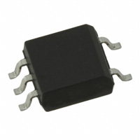
Analog High Speed Optocoupler, 1 MBd, Transistor Output, SOP-5 Package
FEATURES
• Surface mountable
A1 6 VCC 5C C3
20409-2
• Industry standard SOP-5 footprint • Compatible with infrared vapor phase reflow and wave soldering processes • Isolation test voltage, 3750 VRMS • Very high common mode transient immunity: 15 000 V/µs at VCM = 1500 V guaranteed (VOM453T) • High speed: 1 MBd • TTL compatible • Open collector output
4E
20409-1
DESCRIPTION
The VOM452T and VOM453T, high speed optocouplers, each consists of a GaAlAs infrared emitting diode, optically coupled with an integrated photo detector and a high speed transistor. The photo detector is junction isolated from the transistor to reduce miller capacitance effects. The open collector output function allows circuit designers to adjust the load conditions when interfacing with different logic systems such as TTL, CMOS, etc. Because the VOM452T and VOM453T have a Faraday shield on the detector chip, it can also reject and minimize high input to output common mode transient voltages. There is no base connection, further reducing the potential electrical noise entering the package. The VOM452T and VOM453T are packaged in industry standard SOP-5 packages and are suitable for surface mounting.
• Compliant to RoHS directive 2002/95/EC accordance to WEEE 2002/96/EC
and
in
APPLICATIONS
• Fieldbus communication and control • Logic ground isolation • Analog signal ground isolation • Replace pulse transformers
AGENCY APPROVALS
• UL1577, file no. E52744 system code U • cUL - file no. E52744, equivalent to CSA bulletin 5A
ORDERING INFORMATION
SOP-5
V
O
M
4 PART NUMBER
5
#
T
7.21 mm
AGENCY CERTIFIED/PACKAGE UL, cUL SOP-5 ≥ 15 VOM452T
CTR (%) ≥ 15 VOM453T ≥1
CMTI (kV/µs) ≥ 15 VOM453T VOM452T
Note • For additional information on the available options refer to option information. The product is available only on tape and reel.
Document Number: 81587 Rev. 1.0, 08-Apr-10
For technical questions, contact: optocoupleranswers@vishay.com
www.vishay.com 1
�VOM452T, VOM453T
Vishay Semiconductors Analog High Speed Optocoupler, 1 MBd,
Transistor Output, SOP-5 Package
ABSOLUTE MAXIMUM RATINGS (Tamb = 25 °C, unless otherwise specified)
PARAMETER INPUT Reverse voltage DC forward current Surge forward current Power dissipation OUTPUT Supply voltage Output voltage Output current Power dissipation COUPLER Isolation test voltage between emitter and detector (refer to climate DIN 40046, part 2, Nov. 74) Pollution degree (DIN VDE 0110) Creepage distance Clearance distance Comparative tracking index per DIN IEC 112/VDE 0303, part 1 Isolation resistance Storage temperature range Ambient temperature range Junction temperature Soldering temperature (2) t < 10 s max. VIO = 500 V, Tamb = 25 °C, RISOL
(1)
TEST CONDITION
SYMBOL VR IF
VALUE 3 25 1 45 - 0.5 to 30 - 0.5 to 25 8 100
UNIT V mA A mW V V mA mW
tp ≤ 1 µs, 300 pulses/s Tamb ≤ 70 °C
IFSM Pdiss VS VO IO
Tamb ≤ 70 °C
Pdiss
t=1s
VISO
3750 2 ≥5 ≥5 175
VRMS
mm mm
RIO RIO Tstg Tamb Tj
≥ 1012 ≥ 1011 - 55 to + 125 - 55 to + 100 100 260
Ω Ω °C °C °C °C
VIO = 500 V, Tamb = 100 °C, RISOL (1)
Notes • Stresses in excess of the absolute maximum ratings can cause permanent damage to the device. Functional operation of the device is not implied at these or any other conditions in excess of those given in the operational sections of this document. Exposure to absolute maximum ratings for extended periods of the time can adversely affect reliability. (1) Device considered a two-terminal device: pins 1, and 3 shorted together and pins 4, 5, and 6 shorted together. (2) Refer to reflow profile for soldering conditions for surface mounted devices.
www.vishay.com 2
For technical questions, contact: optocoupleranswers@vishay.com
Document Number: 81587 Rev. 1.0, 08-Apr-10
�VOM452T, VOM453T
Analog High Speed Optocoupler, 1 MBd, Vishay Semiconductors Transistor Output, SOP-5 Package
ELECTRICAL CHARACTERISTICS (Tamb = 25 °C, unless otherwise specified)
PARAMETER INPUT Input forward voltage Input reverse current Input capacitance Temperature coefficient of forward voltage OUTPUT Logic low supply current Logic high supply current IF = 16 mA, VO = open, VCC = 15 V IF = 0 mA, VO = open, VCC = 15 V IF = 0 mA, VO = open, VCC = 15 V, Tamb = 0 °C to 70 °C IF = 16 mA, VCC = 4.5 V, IO = 3 mA Logic low output voltage IF = 16 mA, VCC = 15V, IO = 2.4 mA, Tamb = - 40 °C to + 100 °C IF = 0 mA, VO = VCC = 5.5V Logic high output current IF = 0 mA, VO = VCC = 15V IF = 0 mA, VO = VCC = 15 V, Tamb = 0 °C to 70 °C COUPLER Capacitance (input-output) (1) f = 1 MHz CIO 0.4 pF Notes • Minimum and maximum values are testing requirements. Typical values are characteristics of the device and are the result of engineering evaluation. Typical values are for information only and are not part of the testing requirements. (1) A 0.1 µF bypass capacitor connected between pins 4 and 6 is recommended. ICCL ICCH ICCH VOL VOL IOH IOH IOH 0.003 0.01 0.15 200 0.001 1 2 0.4 0.5 0.5 1 50 µA µA µA V V µA µA µA IF = 16 mA VR = 3 V f = 1 MHz, VF = 0 V IF = 16 mA VF IR CIN ΔVF/ΔTamb 1.6 0.5 75 - 1.7 1.8 10 V µA pF mV/°C TEST CONDITION PART SYMBOL MIN. TYP. MAX. UNIT
CURRENT TRANSFER RATIO
PARAMETER Current transfer ratio (1)(2) TEST CONDITION VO = 0.4 V, IF = 16 mA, VCC = 4.5 V SYMBOL CTR MIN. 15 TYP. 30 MAX. UNIT %
Notes (1) Current transfer ratio in percent equals the ratio of output collector current (I ) to the forward LED input current (I ) times 100. O F (2) A 0.1 µF bypass capacitor connected between pins 4 and 6 is recommended.
SWITCHING CHARACTERISTICS (all typical values, Tamb = 25 °C)
PARAMETER Propagation delay time to logic low at output (see fig. 1 and note 1) Propagation delay time to logic high at output (see fig. 1 and note 1) TEST CONDITION RL = 1.9 kΩ RL = 1.9 kΩ SYMBOL tPHL tPLH MIN. TYP. 0.25 0.5 MAX. 1 1 UNIT µs µs
Notes • VCC = 5 V, IF = 16 mA unless otherwise specified. (1) The 1.9 kΩ load represents 1 TTL unit load of 1.6 mA and the 5.6 kΩ pull-up resistor.
10 % duty cycle 1/f < 100 µs Pulse generator ZO = 50 Ω tr = 5 ns IF IF 1 6 RL 5 0.1 µF 3 IF = monitor Rm
20410
+5V
0 VO 5V
VO 1.5 V C L = 15 pF tPHL tPLH 1.5 V VOL
4
Fig. 1 - Test Circuit for Switching Times Document Number: 81587 Rev. 1.0, 08-Apr-10 For technical questions, contact: optocoupleranswers@vishay.com www.vishay.com 3
�VOM452T, VOM453T
Vishay Semiconductors Analog High Speed Optocoupler, 1 MBd,
Transistor Output, SOP-5 Package
COMMON MODE TRANSIENT IMMUNITY
PARAMETER Common mode transient immunity at logic high level output (see fig. 2 and notes 1, and 2) TEST CONDITION RL = 1.9 kΩ, IF = 0 mA, VCM = 10 VP-P, Tamb = 25 °C RL = 1.9 kΩ, IF = 0 mA, VCM = 1500 VP-P, Tamb = 25 °C RL = 1.9 kΩ, IF = 16 mA, VCM = 10 VP-P, Tamb = 25 °C RL = 1.9 kΩ, IF = 16 mA, VCM = 1500 VP-P, Tamb = 25 °C PART VOM452T SYMBOL |CMH| MIN. 1 TYP. MAX. UNIT kV/µs
VOM453T
|CMH|
15
kV/µs
Common mode transient immunity at logic low level output (see fig. 2 and notes 1, and 2)
VOM452T
|CML|
1
kV/µs
VOM453T
|CML|
15
kV/µs
Notes (1) Common mode transient immunity in a logic high level is the maximum tolerable (positive) dV CM/dt on the leading edge of the common mode pulse (VCM) to assure that the output will remain in a logic high state (i.e., VO > 2 V). Common mode transient immunity in a logic low level the maximum tolerable (negative) dVCM/dt on the trailing edge of the common mode pulse signal (VCM to assure that the output will remain in logic low state, i.e., VO > 0.8 V). (2) The 1.9 kΩ load represents 1 TTL unit load of 1.6 mA and the 5.6 kΩ pull-up resistor.
IF 1 6 RL 5 A B VFF VCM +
20411
+5V
VCM 0 V 10 %
90 % tr
90 % 10 % tf
VO 0.1 µF
3
4
Switch at A: IF = 0 mA VO 2V
5V
–
0.8 V VO Switch at B: IF = 16 mA VOL
Pulse Generator
Fig. 2 - Test Circuit for Transient Immunity and Typical Waveforms
SAFETY AND INSULATION RATINGS
PARAMETER Climatic classification (according to IEC 68 part 1) Comparative tracking index Peak transient overvoltage Peak insulation voltage Safety rating - power output Safety rating - input current Safety rating - temperature Creepage distance Clearance distance CTI VIOTM VIORM PSO ISI TSI 5 5 175 6000 707 350 150 175 TEST CONDITION SYMBOL MIN. TYP. 55/100/21 399 V V mW mA °C mm mm MAX. UNIT
Note • As per IEC 60747-5-5, § 7.4.3.8.1, this optocoupler is suitable for “safe electrical insulation” only within the safety ratings. Compliance with the safety ratings shall be ensured by means of prodective circuits.
www.vishay.com 4
For technical questions, contact: optocoupleranswers@vishay.com
Document Number: 81587 Rev. 1.0, 08-Apr-10
�VOM452T, VOM453T
Analog High Speed Optocoupler, 1 MBd, Vishay Semiconductors Transistor Output, SOP-5 Package
TYPICAL CHARACTERISTICS (Tamb = 25 °C, unless otherwise specied)
80
1000
CTR - Current Transfer Ratio
Tp - Propagation Delay (ns)
VCC = 4.5 V VO = 0.4 V 60
800 600
IF = 16 mA, VCC = 5 V, Rg = 1.9 kΩ, Cg = 15 pF Duty cycle = 10 %, f = 10 kHz
40
tPLH 400 200 tPHL
20
0 0
22101
5
10
15
20
21876
0 - 40
- 20
0
20
40
60
80
100
IF - Forward Current (mA)
TA - Temperature (°C)
Fig. 3 - Current Transfer Ratio vs. Forward Current
Fig. 6 - Propagation Delay vs. Temperature
25
1000
IF - LED Current (mA)
20 0 °C 15 10
IOH - Output Current (nA)
25 °C
IF = 0 mA 100
10 VCC = VO = 15 V 1 VCC = VO = 5.5 V 0.1 - 40
75 °C - 40 °C
5 0 1 1.1 1.2 1.3 1.4 1.5 1.6 1.7
- 20
0
20
40
60
80
100
21874-1
VF - LED Forward Voltage (V)
21877
TA - Temperature (°C)
Fig. 4 - LED Current vs. LED Forward Voltage
Fig. 7 - Logic High Output Current vs. Temperature
80
500
IO - Output Current (mA)
70 60 50 40 30 20 10 0 - 40
ICCL - Supply Current (µA)
IF = 20 mA IF = 16 mA IF = 10 mA IF = 5 mA IF = 2 mA
VCC = 4.5 V VO = 0.4 V
400 300 200 100 0 - 40
IF = 16 mA VCC = 15 V VO = open
IF = 1 mA
- 20
0
20
40
60
80
100
21878
- 20
0
20
40
60
80
100
21875
Temperature (°C)
Fig. 5 - Output Current vs. Temperature
TA - Temperature (°C)
Fig. 8 - Supply Current vs. Temperature
Document Number: 81587 Rev. 1.0, 08-Apr-10
For technical questions, contact: optocoupleranswers@vishay.com
www.vishay.com 5
�VOM452T, VOM453T
Vishay Semiconductors Analog High Speed Optocoupler, 1 MBd,
Transistor Output, SOP-5 Package
400
VOL - Output Voltage (V)
350 300 250 200
IF = 16 mA VCC = 4.5 V
IO = 3 mA
IO = 2.4 mA 150 100 - 40
- 20
0
20
40
60
80
100
21879
TA- Temperature (°C)
Fig. 9 - Logic Low Output Voltage vs. Temperature
PACKAGE DIMENSIONS in millimeters
6 5 4
ISO Method A
4.83 4.32
0.36
R 0.25 1.27 2.54 1.27
0.91
1 3
Pin one I.D. (on chamfer side of package) 4.67 4.17 0.61 0.86 2.03 1.91 6° 0.46 0.33 0.20 0.10 40°
5.08 7.37
5.59 5.08 10°
1.14
0.46 0.36 1.335 1.205
Leads coplanarity 0.10 max. 1.335 1.205 7.21 6.71
0.63 0.38
2.67 2.41
20643
PACKAGE MARKING
M452 V YWW U 68
21764-54
www.vishay.com 6
For technical questions, contact: optocoupleranswers@vishay.com
Document Number: 81587 Rev. 1.0, 08-Apr-10
�Legal Disclaimer Notice
Vishay
Disclaimer
All product specifications and data are subject to change without notice. Vishay Intertechnology, Inc., its affiliates, agents, and employees, and all persons acting on its or their behalf (collectively, “Vishay”), disclaim any and all liability for any errors, inaccuracies or incompleteness contained herein or in any other disclosure relating to any product. Vishay disclaims any and all liability arising out of the use or application of any product described herein or of any information provided herein to the maximum extent permitted by law. The product specifications do not expand or otherwise modify Vishay’s terms and conditions of purchase, including but not limited to the warranty expressed therein, which apply to these products. No license, express or implied, by estoppel or otherwise, to any intellectual property rights is granted by this document or by any conduct of Vishay. The products shown herein are not designed for use in medical, life-saving, or life-sustaining applications unless otherwise expressly indicated. Customers using or selling Vishay products not expressly indicated for use in such applications do so entirely at their own risk and agree to fully indemnify Vishay for any damages arising or resulting from such use or sale. Please contact authorized Vishay personnel to obtain written terms and conditions regarding products designed for such applications. Product names and markings noted herein may be trademarks of their respective owners.
Document Number: 91000 Revision: 18-Jul-08
www.vishay.com 1
�