W25X10BVZPIG

W25X10BVZPIG

  • 厂商:

    WINBOND(华邦)

  • 封装:

    WSON-8-EP(5x6)

  • 描述:

    IC FLASH 1MBIT SPI 104MHZ 8WSON

  • 详情介绍
  • 数据手册
  • 价格&库存
W25X10BVZPIG 数据手册
W25X10BV/20BV/40BV 1M-BIT, 2M-BIT AND 4M-BIT SERIAL FLASH MEMORY WITH 4KB SECTORS AND DUAL I/O SPI - 1- Publication Release Date: August 20,, 2009 Preliminary -- Revision B W25X10BV/20BV/40BV Table of Contents 1. 2. 3. 4. 5. 6. GENERAL DESCRIPTION ......................................................................................................... 4 FEATURES ................................................................................................................................. 4 PIN CONFIGURATION SOIC 150-MIL / 208-MIL ...................................................................... 5 PAD CONFIGURATION WSON 6X5-MM .................................................................................. 5 PIN CONFIGURATION PDIP 300-MIL ....................................................................................... 6 PIN DESCRIPTION SOIC 150 / 208-MIL, PDIP 300-MIL, WSON 6X5-MM............................... 6 6.1 6.2 6.3 6.4 6.5 6.6 7. 8. Package Types ............................................................................................................... 7 Chip Select (/CS) ............................................................................................................ 7 Serial Data Input, Output and IOs (DI, DO, IO0 and IO1) .............................................. 7 Write Protect (/WP) ......................................................................................................... 7 HOLD (/HOLD) ............................................................................................................... 7 Serial Clock (CLK) .......................................................................................................... 7 BLOCK DIAGRAM ...................................................................................................................... 8 FUNCTIONAL DESCRIPTION ................................................................................................... 9 8.1 SPI OPERATIONS ......................................................................................................... 9 8.1.1 8.1.2 8.1.3 Standard SPI Instructions .................................................................................................9 Dual SPI Instructions ........................................................................................................9 Hold Function ...................................................................................................................9 Write Protect Features....................................................................................................10 8.2 9. WRITE PROTECTION.................................................................................................. 10 8.2.1 CONTROL AND STATUS REGISTERS ................................................................................... 11 9.1 STATUS REGISTER .................................................................................................... 11 9.1.1 9.1.2 9.1.3 9.1.4 9.1.5 9.1.6 9.1.7 BUSY..............................................................................................................................11 Write Enable Latch (WEL) ..............................................................................................11 Block Protect Bits (BP2, BP1, BP0) ................................................................................11 Top/Bottom Block Protect (TB) .......................................................................................11 Reserved Bits .................................................................................................................11 Status Register Protect (SRP) ........................................................................................12 Status Register Memory Protection ................................................................................13 Manufacturer and Device Identification ..........................................................................14 Instruction Set ................................................................................................................15 Write Enable (06h)..........................................................................................................16 Write Disable (04h) .........................................................................................................16 Read Status Register (05h) ............................................................................................17 Write Status Register (01h) ............................................................................................18 Read Data (03h) .............................................................................................................19 Fast Read (0Bh) .............................................................................................................20 9.2 INSTRUCTIONS ........................................................................................................... 14 9.2.1 9.2.2 9.2.3 9.2.4 9.2.5 9.2.6 9.2.7 9.2.8 -2- W25X10BV/20BV/40BV 9.2.9 9.2.10 9.2.11 9.2.12 9.2.13 9.2.14 9.2.15 9.2.16 9.2.17 9.2.18 9.2.19 9.2.20 9.2.21 9.2.22 9.2.23 Fast Read Dual Output (3Bh) .........................................................................................21 Fast Read Dual I/O (BBh).............................................................................................22 Continuous Read Mode Bits (M7-0) .............................................................................24 Continuous Read Mode Reset (FFFFh) .......................................................................24 Page Program (02h) .....................................................................................................25 Sector Erase (20h) .......................................................................................................26 32KB Block Erase (52h) ...............................................................................................27 Block Erase (D8h) ........................................................................................................28 Chip Erase (C7h or 60h) ...............................................................................................29 Power-down (B9h) ........................................................................................................30 Release Power-down / Device ID (ABh) .......................................................................31 Read Manufacturer / Device ID (90h) ...........................................................................33 Read Manufacturer / Device ID Dual I/O (92h) .............................................................34 Read Unique ID Number (4Bh).....................................................................................35 JEDEC ID (9Fh) ...........................................................................................................36 10. ELECTRICAL CHARACTERISTICS ......................................................................................... 37 10.1 10.2 10.3 10.4 10.5 10.6 10.7 10.8 10.9 10.10 Absolute Maximum Ratings .......................................................................................... 37 Operating Ranges......................................................................................................... 37 Power-up Timing and Write Inhibit Threshold .............................................................. 38 DC Electrical Characteristics ........................................................................................ 39 AC Measurement Conditions ........................................................................................ 40 AC Electrical Characteristics ........................................................................................ 41 AC Electrical Characteristics (cont’d) ........................................................................... 42 Serial Output Timing ..................................................................................................... 43 Input Timing .................................................................................................................. 43 Hold Timing ................................................................................................................. 43 8-Pin SOIC 150-mil (Package Code SN)...................................................................... 44 8-Pin SOIC 208-mil (Package Code SS) ...................................................................... 45 8-Pin PDIP 300-mil (Package Code DA) ...................................................................... 46 8-Contact 6x5mm WSON (Package Code ZP) ............................................................ 47 Valid Part Numbers and Top Side Marking .................................................................. 50 11. PACKAGE SPECIFICATION .................................................................................................... 44 11.1 11.2 11.3 11.4 12. ORDERING INFORMATION .................................................................................................... 49 12.1 REVISION HISTORY ............................................................................................................................ 51 -3- Publication Release Date: August 20, 2009 Preliminary -- Revision B W25X10BV/20BV/40BV 1. GENERAL DESCRIPTION The W25X10BV (1M-bit), W25X20BV (2M-bit) and the W25X40BV (4M-bit) Serial Flash memories provides a storage solution for systems with limited space, pins and power. The 25X series offers flexibility and performance well beyond ordinary Serial Flash devices. They are ideal for code download applications as well as storing voice, text and data. The devices operate on a single 2.7V to 3.6V power supply with current consumption as low as 4mA active and 1µA for power-down. All devices are offered in space-saving packages. The W25X10BV/20BV/40BV arrays are organized into 512/1,024/2,048 programmable pages of 256bytes each. Up to 256 bytes can be programmed at a time using the Page Program instruction. Pages can be erased in groups of 16 (sector erase), groups of 128 (32KB block erase), groups of 256 (block erase) or the entire chip (chip erase). The W25X10BV/20BV/40BV has 32/64/128 erasable sectors and 2/4/8 erasable 64KB blocks respectively. The small 4KB sectors allow for greater flexibility in applications that require data and parameter storage. (See figure 2.) The W25X10BV/20BV/40BV supports the standard Serial Peripheral Interface (SPI), and a high performance dual output as well as Dual I/O SPI: Serial Clock, Chip Select, Serial Data DI (I/O0), DO (I/O1). SPI clock frequencies of up to 104MHz are supported allowing equivalent clock rates of 208MHz when using the Fast Read Dual Output instruction. These transfer rates are comparable to those of 8 and 16-bit Parallel Flash memories. A Hold pin, Write Protect pin and programmable write protect, with top or bottom array control features, provide further control flexibility. Additionally, the device supports JEDEC standard manufacturer and device identification. 2. FEATURES  Family of Serial Flash Memories – W25X10BV: 1M-bit/128K-byte (131,072) – W25X20BV: 2M-bit/256K-byte (262,144) – W25X40BV: 4M-bit/512K-byte (524,288) – 256-bytes per programmable page – Uniform 4KB Sectors, 32KB & 64KB Blocks  SPI with Single / Dual Outputs / Dual I/O – Clock, Chip Select, Data I/O, Data Out – Optional Hold function for SPI flexibility  Data Transfer up to 208M-bits / second – Clock operation to 104MHz – Fast Read Dual Output instruction – Auto-increment Read capability  Efficient “Continuous Read Mode” – Low Instruction overhead – Continuous Read – As few as 8 clocks to address memory – Allows true XIP (execute in place) operation  Softw are and Hardware Write Protection – Write-Protect all or portion of memory – Enable/Disable protection with /WP pin – Top or bottom array protection  Flexible Architecture w ith 4KB sectors – Sector Erase (4K-bytes) – Block Erase (32K and 64K-byte) – Page program up to 256 bytes
W25X10BVZPIG
物料型号: - W25X10BV:1M-bit/128K-byte - W25X20BV:2M-bit/256K-byte - W25X40BV:4M-bit/512K-byte

器件简介: W25X系列提供了适用于空间、引脚和功耗受限系统的存储解决方案。它们适用于代码下载应用以及存储声音、文本和数据。这些设备在2.7V至3.6V的单电源下工作,活动时电流消耗低至4mA,掉电模式下为1µA。所有设备都提供节省空间的封装。

引脚分配: - SOIC 150-MIL / 208-MIL:8引脚,包括Chip Select(/CS)、Data Input/Output(DI/DO)、Write Protect(/WP)、Ground(GND)、Serial Clock(CLK)、Hold(/HOLD)和Power Supply(VCC)。 - 
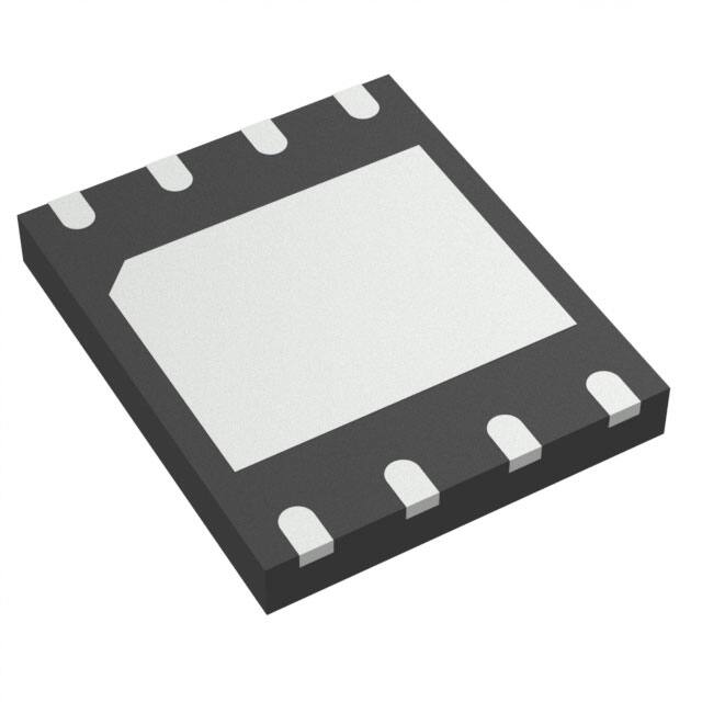
WSON 6X5-MM:8接触点,配置与SOIC相似。 - PDIP 300-MIL:8引脚DIP封装,引脚配置与SOIC封装相同。

参数特性: - 程序页面:512/1,024/2,048个,每个256字节。 - 可擦除扇区:32/64/128个,大小为4KB。 - 可擦除块:2/4/8个,大小为64KB。 - 支持SPI时钟频率高达104MHz,Fast Read Dual Output指令下等效时钟频率208MHz。

功能详解: - 支持标准SPI和双输出/双I/O SPI操作。 - 提供数据传输速率最高达208M-bits/秒。 - 支持软件和硬件写保护。 - 支持4KB扇区擦除、32KB和64KB块擦除。 - 低功耗,宽温度范围工作,提供2.7至3.6V单电源。 - 封装类型包括8-pin SOIC 150-mil、8-pin SOIC 208-mil、8-pad WSON 6x5-mm和8-pin PDIP 300-mil。

应用信息: 适用于需要数据和参数存储的应用,提供灵活的架构和高效的“连续读取模式”,支持真正的XIP(现场执行)操作。

封装信息: - 8-pin塑料150-mil宽度SOIC(封装代码SN)。 - 6x5-mm WSON(封装代码ZP)。 - 208-mil宽度SOIC(封装代码SS)。 - 300-mil 8-pin PDIP(封装代码DA)。
W25X10BVZPIG 价格&库存

很抱歉,暂时无法提供与“W25X10BVZPIG”相匹配的价格&库存,您可以联系我们找货

免费人工找货