0
登录后你可以
  • 下载海量资料
  • 学习在线课程
  • 观看技术视频
  • 写文章/发帖/加入社区
会员中心
创作中心
发布
  • 发文章

  • 发资料

  • 发帖

  • 提问

  • 发视频

创作活动
W25X20

W25X20

  • 厂商:

    WINBOND(华邦)

  • 封装:

  • 描述:

    W25X20 - 1M-BIT, 2M-BIT, 4M-BIT AND 8M-BIT SERIAL FLASH MEMORY WITH 4KB SECTORS AND DUAL OUTPUT SPI ...

  • 详情介绍
  • 数据手册
  • 价格&库存
W25X20 数据手册
W25X10, W25X20, W25X40, W25X80 1M-BIT, 2M-BIT, 4M-BIT AND 8M-BIT SERIAL FLASH MEMORY WITH 4KB SECTORS AND DUAL OUTPUT SPI -1- Publication Release Date: September 22, 2006 Preliminary - Revision I W25X10, W25X20, W25X40, W25X80 Table of Contents1. 2. 3. 4. 5. 6. 7. GENERAL DESCRIPTION ......................................................................................................... 4 FEATURES ................................................................................................................................. 4 PIN CONFIGURATION SOIC 150-MIL....................................................................................... 5 PIN CONFIGURATION SOIC 208-MIL....................................................................................... 5 PIN CONFIGURATION PDIP 300-MIL ....................................................................................... 5 PIN CONFIGURATION WSON 6X5-MM .................................................................................... 6 PIN DESCRIPTION..................................................................................................................... 6 7.1 7.2 7.3 7.4 7.5 7.6 7.7 8. 9. Package Types ............................................................................................................... 7 Chip Select (/CS) ............................................................................................................ 7 Serial Data Output (DO) ................................................................................................. 7 Write Protect (/WP)......................................................................................................... 7 HOLD (/HOLD) ............................................................................................................... 7 Serial Clock (CLK) .......................................................................................................... 7 Serial Data Input / Output (DIO) ..................................................................................... 7 BLOCK DIAGRAM ...................................................................................................................... 8 FUNCTIONAL DESCRIPTION ................................................................................................... 9 9.1 SPI OPERATIONS ......................................................................................................... 9 9.1.1 9.1.2 9.1.3 SPI Modes ........................................................................................................................9 Dual Output SPI................................................................................................................9 Hold Function ...................................................................................................................9 Write Protect Features....................................................................................................10 9.2 10. WRITE PROTECTION.................................................................................................. 10 9.2.1 CONTROL AND STATUS REGISTERS................................................................................... 11 10.1 STATUS REGISTER .................................................................................................... 11 10.1.1 10.1.2 10.1.3 10.1.4 10.1.5 10.1.6 10.1.7 BUSY............................................................................................................................11 Write Enable Latch (WEL) ............................................................................................11 Block Protect Bits (BP2, BP1, BP0)..............................................................................11 Top/Bottom Block Protect (TB) .....................................................................................11 Reserved Bits ...............................................................................................................11 Status Register Protect (SRP) ......................................................................................12 Status Register Memory Protection ..............................................................................13 Manufacturer and Device Identification.........................................................................14 Instruction Set (1) ...........................................................................................................15 Write Ensable (06h)......................................................................................................16 Write Disable (04h).......................................................................................................16 10.2 INSTRUCTIONS........................................................................................................... 14 10.2.1 10.2.2 10.2.3 10.2.4 -2- W25X10, W25X20, W25X40, W25X80 10.2.5 10.2.6 10.2.7 10.2.8 10.2.9 10.2.10 10.2.11 10.2.12 10.2.13 10.2.14 10.2.15 10.2.16 10.2.17 Read Status Register (05h) ..........................................................................................17 Write Status Register (01h) ..........................................................................................18 Read Data (03h) ...........................................................................................................19 Fast Read (0Bh) ...........................................................................................................20 Fast Read Dual Output (3Bh) .......................................................................................21 Page Program (02h) ...................................................................................................22 Sector Erase (20h) .....................................................................................................23 Block Erase (D8h) ......................................................................................................24 Chip Erase (C7h)........................................................................................................25 Power-down (B9h) ......................................................................................................26 Release Power-down / Device ID (ABh) .....................................................................27 Read Manufacturer / Device ID (90h) .........................................................................29 JEDEC ID (9Fh)..........................................................................................................30 11. ELECTRICAL CHARACTERISTICS (PRELIMINARY) (4) ....................................................... 31 11.1 Absolute Maximum Ratings (1) .................................................................................... 31 11.2 11.3 11.4 11.5 11.6 11.7 11.8 11.9 11.10 11.11 Operating Ranges......................................................................................................... 31 Endurance and Data Retention .................................................................................... 32 Power-up Timing and Write Inhibit Threshold .............................................................. 32 DC Electrical Characteristics ........................................................................................ 33 AC Measurement Conditions........................................................................................ 34 AC Electrical Characteristics ........................................................................................ 35 AC Electrical Characteristics (cont’d) ........................................................................... 36 Serial Output Timing ..................................................................................................... 37 Input Timing................................................................................................................. 37 Hold Timing ................................................................................................................. 37 8-Pin SOIC 150-mil (Package Code SN)...................................................................... 38 8-Pin SOIC 208-mil (Package Code SS)...................................................................... 39 8-Pin PDIP 300-mil (Package Code DA) ...................................................................... 40 8-contact 6x5 WSON .................................................................................................... 41 8-contact 6x5 WSON Cont’d. ....................................................................................... 42 12. PACKAGE SPECIFICATION .................................................................................................... 38 12.1 12.2 12.3 12.4 12.5 13. 14. ORDERING INFORMATION (1)................................................................................................. 43 REVISION HISTORY ................................................................................................................ 44 -3- Publication Release Date: September 22, 2006 Preliminary - Revision I W25X10, W25X20, W25X40, W25X80 1. GENERAL DESCRIPTION The W25X10 (1M-bit), W25X20 (2M-bit), W25X40 (4M-bit) and W25X80 (8M-bit) Serial Flash memories provide a storage solution for systems with limited space, pins and power. The 25X series offers flexibility and performance well beyond ordinary Serial Flash devices. They are ideal for code download applications as well as storing voice, text and data. The devices operate on a single 2.7V to 3.6V power supply with current consumption as low as 5mA active and 1µA for power-down. All devices are offered in space-saving packages. The W25X10/20/40/80 array is organized into 512/1024/2048/4096 programmable pages of 256-bytes each. Up to 256 bytes can be programmed at a time using the Page Program instruction. Pages can be erased in groups of 16 (sector erase), groups of 256 (block erase) or the entire chip (chip erase). The W25X10/20/40/80 has 32/64/128/256 erasable sectors and 2/4/8/16 erasable blocks respectively. The small 4KB sectors allow for greater flexibility in applications that require data and parameter storage. (See figure 2.) The W25X10/20/40/80 supports the standard Serial Peripheral Interface (SPI), and a high performance dual output SPI using four pins: Serial Clock, Chip Select, Serial Data I/O and Serial Data Out. SPI clock frequencies of up to 75MHz are supported allowing equivalent clock rates of 150MHz when using the Fast Read Dual Output instruction. These transfer rates are comparable to those of 8 and 16-bit Parallel Flash memories. A Hold pin, Write Protect pin and programmable write protect, with top or bottom array control features, provide further control flexibility. Additionally, the device supports JEDEC standard manufacturer and device identification. 2. FEATURES • Family of Serial Flash Memories – W25X10: 1M-bit / 128K-byte (131,072) – W25X20: 2M-bit / 256K-byte (262,144) – W25X40: 4M-bit / 512K-byte (524,288) – W25X80: 8M-bit / 1M-byte (1,048,576) – 256-bytes per programmable page – Uniform 4K-byte Sectors / 64K-byte Blocks • SPI with Single or Dual Outputs – Clock, Chip Select, Data I/O, Data Out – Optional Hold function for SPI flexibility • Data Transfer up to 150M-bits / second – Clock operation to 75MHz – Fast Read Dual Output instruction – Auto-increment Read capability • Flexible Architecture with 4KB sectors – Sector Erase (4K-bytes) – Block Erase (64K-byte) – Page program up to 256 bytes
W25X20
### 物料型号 - W25X10 (1M-BIT) - W25X20 (2M-BIT) - W25X40 (4M-BIT) - W25X80 (8M-BIT)

### 器件简介 W25X系列提供了适用于空间、引脚和功耗受限系统的存储解决方案。这些设备在单2.7V至3.6V电源下工作,活动时电流消耗低至5mA,掉电模式下为1µA。所有设备都提供节省空间的封装。

### 引脚分配 - SOIC 150-mil:包括W25X10、W25X20和W25X40。 - SOIC 208-mil:包括W25X40和W25X80。 - PDIP 300-mil:包括W25X10、W25X20、W25X40和W25X80。 - WSON 6x5-mm:包括W25X10、W25X20、W25X40和W25X80。

### 参数特性 - 支持SPI标准和双输出SPI。 - 支持高达75MHz的SPI时钟频率。 - 支持快速读取双输出指令,等效于150MHz的时钟速率。 - 具有32/64/128/256个可擦除扇区和2/4/8/16个可擦除块。 - 提供标准的制造商和设备识别。

### 功能详解 - SPI操作:支持SPI模式0和3。 - 双输出SPI:使用“快速读取双输出”指令时支持。 - 保持功能:/HOLD引脚允许在设备被选中时暂停操作。 - 写保护:提供软件和硬件写保护功能。

### 应用信息 适用于代码下载应用以及存储语音、文本和数据。

### 封装信息 - 
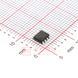
8-pin SOIC 150-mil (W25X10/20/40) - 8-pin SOIC 208-mil (W25X40/80) - 8-pin PDIP 300-mil (W25X10/20/40/80) - 
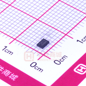
8-contact 6x5 WSON (W25X10/20/40/80)
W25X20 价格&库存

很抱歉,暂时无法提供与“W25X20”相匹配的价格&库存,您可以联系我们找货

免费人工找货
W25X20CLSNIG
  •  国内价格
  • 1+2.41921
  • 10+2.32321
  • 100+2.09281
  • 500+1.97761

库存:335

W25X20CLUXIG TR
  •  国内价格
  • 1+1.624
  • 30+1.568
  • 100+1.456
  • 500+1.344
  • 1000+1.288

库存:493