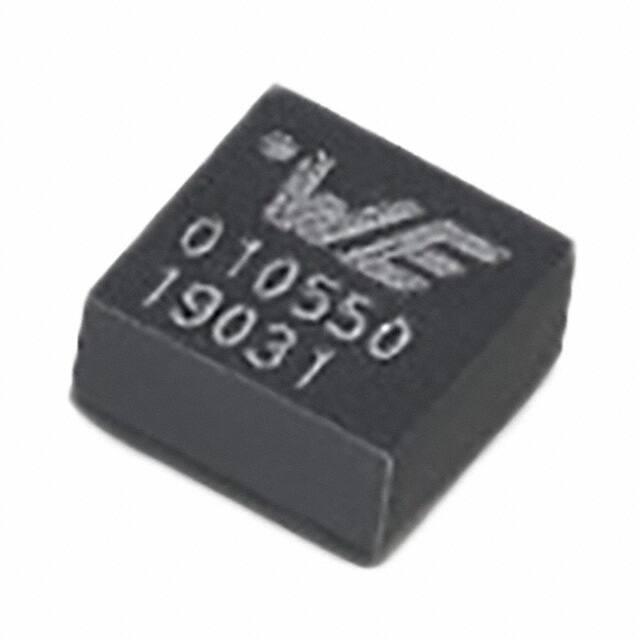
171010550
MagI3 C Power Module
VDMM - Variable Step Down MicroModule
2.5V - 5.5V Input / 1.2A Output / 0.8V - 5.5V Output
DESCRIPTION
FEATURES
The VDMM 171010550 MagI3 C MicroModule provides
a fully integrated DC-DC power supply including the
switching regulator IC with integrated MOSFETs,
controller, compensation and shielded inductor in one
package.
•
•
•
•
•
•
•
•
•
•
•
•
•
•
•
•
•
•
•
•
•
The 171010550 offers high efficiency and delivers
up to 1.2A of output current. It operates with an input
voltage from 2.5V to 5.5V and is designed for a small
solution size.
The selectable forced COT or power save mode
allows for the choice between high efficiency and low
output voltage ripple at light load.
The 171010550 is available in an LGA-6EP package
(2.5 x 2.5 x 1.2mm).
This module has integrated protection circuitry
that guards against thermal overstress with thermal
shutdown and protects against electrical damage using
overcurrent, short-circuit and undervoltage protections.
Peak efficiency up to 96%
Current capability up to 1.2A
Input voltage range: 2.5V to 5.5V
Output voltage range: 0.8V to 5.5V
25µA typical quiescent current
Integrated shielded inductor
Low output voltage ripple: ±6mV typ.
Output voltage accuracy over temperature: 2% max
Fixed switching frequency: 4MHz
Constant on-time control
Synchronous operation
Selectable forced COT or power save mode
Undervoltage lockout
Internal soft-start
Thermal shutdown
Short-circuit protection
Cycle-by-cycle current limit
RoHS und REACh compliant
Operating ambient temperature up to 85°C
Operating junction temp. range: -40°C to 125°C
Complies with EN55032 class B radiated emissions
standard
TYPICAL APPLICATIONS
• General point of load power supply for low power
systems
• Replacement of linear regulators
• DSP and FPGA power supply auxiliary voltages
• Portable instruments
• Battery powered equipment
TYPICAL CIRCUIT DIAGRAM
VIN
4
3
CIN
2
Module
VIN
Data Sheet version 2.1
www.we-online.com/powermodules
6
VOUT
RFBT
EN
FB
MODE
PGND
GND
VOUT
EP
PGND
5
1
CFF
COUT
RFBB
GND
© March 2022
1
�171010550
MagI3 C Power Module
VDMM - Variable Step Down MicroModule
PINOUT
MARKING
DESCRIPTION
°WE
Pin 1 Indicator and Logo
010550
Order Code
XXYYZ
Year, Week and Lot Number
SYMBOL
NUMBER
TYPE
DESCRIPTION
FB
1
Input
Feedback pin. This pin must be connected to the external resistor divider
(between VOUT and PGND) to adjust the output voltage.
MODE
2
Input
Forced COT or power save mode selection pin. Settings this pin high, the
forced PWM mode is selected for every load current. Settings this pin low,
PFM/PWM is selected, with the transition automatically occurring
between the two operationing modes according to the load. This pin must
not be left floating.
EN
3
Input
Enable pin. Setting this pin high enables the device, while setting this pin
low shuts down the device. This pin must not be left floating.
VIN
4
Power
Input voltage. Place the input capacitor as close as possible to VIN and
PGND.
PGND
5
Power
Power ground. It must be connected to the ground plane and to the
exposed pad.
VOUT
6
Power
Output voltage. Place output capacitors as close as possible to VOUT and
PGND. For thermal performance, use copper plane(s) at this pin.
PGND
EP
Exposed
Pad
Exposed pad. This pin is internally electrically connected to PGND. It is
recommended to connect it to the ground plane for device heat dissipation.
Data Sheet version 2.1
www.we-online.com/powermodules
© March 2022
2
�171010550
MagI3 C Power Module
VDMM - Variable Step Down MicroModule
ORDERING INFORMATION
ORDER CODE
SPECIFICATIONS
PACKAGE
PACKAGING UNIT
171010550
1.2A / 0.8V-5.5V Vout version
LGA-6EP
7” Reel (1000 pieces)
178010550
1.2A / 0.8V-5.5V Vout version
Eval Board
Box with 1 piece
SALES INFORMATION
SALES CONTACT
Würth Elektronik eiSos GmbH & Co. KG
EMC and Inductive Solutions
Max-Eyth-Str. 1
74638 Waldenburg
Germany
Tel. +49 (0) 7942 945 0
www.we-online.com/powermodules
Technical support: powermodules@we-online.com
Data Sheet version 2.1
www.we-online.com/powermodules
© March 2022
3
�171010550
MagI3 C Power Module
VDMM - Variable Step Down MicroModule
ABSOLUTE MAXIMUM RATINGS
Caution:
Exceeding the listed absolute maximum ratings may affect the device negatively and may cause permanent damage.
SYMBOL
VIN
LIMIT
MIN
MAX(1)
PARAMETER
(1)
UNIT
Input Voltage
-0.3
6
V
Output Voltage
-0.3
VIN -0.3
V
FB
Feedback
-0.3
VIN -0.3
V
EN
Enable
-0.3
VIN -0.3
V
MODE
Power Good
-0.3
VIN -0.3
V
Tstorage
Assembled, non-operating storage temperature
-40
85
°C
ESD Voltage (HBM), all pins (C=100pF, R=1.5kΩ)
-4
4
kV
VOUT
Vesd
OPERATING CONDITIONS
Operating conditions are conditions under which the device is intended to be functional. All values are referenced to GND.
MIN and MAX limits are valid for the recommended ambient temperature range of -40°C to 85°C.
SYMBOL
VIN
VOUT
MIN(1)
TYP(3)
MAX(1)
UNIT
Input Voltage
2.5
-
5.5
V
Output Voltage
0.8
-
5.5
V
PARAMETER
(2)
°C
Ta
Ambient temperature range
-40
-
85
Tjop
Junction temperature range
-40
-
125
°C
Iout
Nominal output current
-
-
1.2
A
THERMAL SPECIFICATIONS
Caution:
Exceeding the listed absolute maximum ratings may affect the device negatively and may cause permanent damage.
SYMBOL
PARAMETER
(4)
ΘJA
Junction-to-ambient thermal resistance
ΘJC
Junction-to-case (top) thermal resistance
TSD
Thermal shutdown, rising
Thermal shutdown, hysteresis
Data Sheet version 2.1
www.we-online.com/powermodules
(4)
TYP(3)
UNIT
150
K/W
82
K/W
160
10
°C
°C
© March 2022
4
�171010550
MagI3 C Power Module
VDMM - Variable Step Down MicroModule
ELECTRICAL SPECIFICATIONS
Caution:
MIN and MAX limits are valid for the recommended ambient temperature range of -40°C to 85°C. Typical values represents
statistically the utmost probable values at the following conditions: VIN =5V, VOUT = 1.8V, CIN = 4.7µF ceramic, COUT
= 10µF ceramic, TA = 25°C unless otherwise noted.
SYMBOL
PARAMETER
MIN(1)
TYP(3)
MAX(1)
UNIT
1.5
2.3
3.0
A
0.784
0.8
0.816
V
-
0
50
nA
-
0.04
-0.9
0.2
-
%/V
%/A
-
6
-
mVpp
-
65
-
mVpp
3.6
4
4.4
MHz
VIN increasing
VIN decreasing
2
-
2.25
2
175
2.4
-
V
V
mV
TEST CONDITIONS
Output Current
IOCP
Overcurrent protection
VFB
Reference voltage
IFB
VOUT
Output Voltage
Feedback input bias current
Line regulation
Load regulation
Output voltage ripple
-40°C ≤ TA ≤ 85°C
VIN = VOUT +1V to 5.5V, MODE = low
500mA ≤ ILOAD ≤ 1A
VIN = 3.6V, IOUT = 100mA, MODE =
high, 20MHz BWL(5)
VIN = 3.6V, IOUT = 100mA, MODE =
low, 20MHz BWL(5)
Switching Frequency
fSW
VUVLO
Switching frequency
Enable and Undervoltage Lockout
VIN undervoltage threshold
VIN undervoltage hysteresis
VEN
EN threshold
Enable logic high
Enable logic low
-
0.85
0.75
-
V
V
IEN
EN pin input current
Enable = high
Enable = low
-
0.1
0.1
-
µA
µA
VMODE
MODE threshold
MODE logic high
MODE logic low
-
0.85
0.75
-
V
V
IMODE
MODE input current
MODE = high
MODE = low
-
0.1
0.1
-
µA
µA
Soft-start time
TA = 25°C (rising edge to 95% of
VOUT )
-
128
-
µs
Mode Selection
Soft-Start
tSS
Data Sheet version 2.1
www.we-online.com/powermodules
© March 2022
5
�171010550
MagI3 C Power Module
VDMM - Variable Step Down MicroModule
Caution:
MIN and MAX limits are valid for the recommended ambient temperature range of -40°C to 85°C. Typical values represents
statistically the utmost probable values at the following conditions: VIN =5V, VOUT = 1.8V, CIN = 4.7µF ceramic, COUT
= 10µF ceramic, TA = 25°C unless otherwise noted.
SYMBOL
PARAMETER
TEST CONDITIONS
MIN(1)
TYP(3)
MAX(1)
UNIT
-
87
-
%
-
90
-
%
-
88
-
%
-
90
-
%
-
96
-
%
-
0.1
0.09
-
µA
µA
-
13
-
mA
-
25
-
µA
-
0.03
-
µA
-
0.03
-
µA
-
220
-
µF
Efficiency
η
Efficiency
VIN = 3.6V, VOUT = 1.8V, IOUT =
50mA, MODE = low
VIN = 5V, VOUT = 3.3V, IOUT =
50mA, MODE = low
VIN = 3.6V, VOUT = 1.8V, IOUT =
200mA, MODE = high
VIN = 5V, VOUT = 3.3V, IOUT =
200mA, MODE = high
VIN = 3.6V, VOUT = 3.3V, IOUT =
200mA, MODE = low
Input Quiescent and Shutdown Current
ISD
IIN
IQ
Shutdown current
VEN = low, VIN = 5V
VEN = low, VIN = 2.5V
No load input current
MODE = high, Enable = high,
switching with no load
MODE = high, Enable = high,
switching with no load
Quiescent current
MODE = high, Enable = high, no
switching, VIN = 2.5V
MODE = high, Enable = high, no
switching
Output Capacitance
COUT_MAX
Maximum output capacitance
Data Sheet version 2.1
www.we-online.com/powermodules
© March 2022
6
�171010550
MagI3 C Power Module
VDMM - Variable Step Down MicroModule
RoHS, REACh
Directive 2011/65/EU of the European Parliament and the Council
of June 8th, 2011 on the restriction of the use of certain hazardous
substances in electrical and electronic equipment.
Directive 1907/2006/EU of the European Parliament and the
Council of June 1st, 2007 regarding the Registration, Evaluation,
Authorization and Restriction of Chemicals (REACh).
RoHS
directive
REACh
directive
PACKAGE SPECIFICATIONS
ITEM
PARAMETER
TYP(3)
UNIT
Mold Compound
UL94V-0
-
-
Weight
-
0.0204
g
NOTES
(1) Min and Max limits are 100% production tested at 25°C. Limits over the operating temperature range are guaranteed through
correlation using Statistical Quality Control (SQC) methods.
(2) Depending on heat sink design, number of PCB layers, copper thickness and air flow.
(3) Typical numbers are valid at 25°C ambient temperature and represent statistically the utmost probable values assuming a
Gaussian distribution.
(4) Measured on the 178010550 evaluation board, a 40 x 40mm two layer board, with 35µm (1 ounce) copper.
(5) The industry standard for comparison of the output voltage ripple between switching regulators or modules requires a 10µF
ceramic (sometimes additional 1µF ceramic in parallel) at the point of load where the voltage measurement is done using
an oscilloscope with its probe and probe jack designed for low voltage/high frequency (low impedance) measurement. The
oscilloscopes bandwidth is limited at 20MHz.
Data Sheet version 2.1
www.we-online.com/powermodules
© March 2022
7
�171010550
MagI3 C Power Module
VDMM - Variable Step Down MicroModule
TYPICAL PERFORMANCE CURVES
If not otherwise specified, the following conditions apply: VIN = 5V, CIN = 4.7µF X5R ceramic, COUT = 10µF X5R ceramic, CFF =
22pF, TAMB = 25°C.
RADIATED EMISSIONS EN55032 (CISPR-32) CLASS B COMPLIANT
Measured with module on an Evaluation Board 178010550 in a Fully Anechoic Room (FAR) at 3m antenna distance.
TEST SETUP
Input wire length:
• Radiated Emission: 160cm (80cm Horizontal + 80cm Vertical)
Output wire length:
• Short wire (with input filter): Load directly on evaluation board
• Long wire (with input filter): 1m
RADIATED BEHAVIOR (without input filter)
Data Sheet version 2.1
www.we-online.com/powermodules
© March 2022
8
�171010550
MagI3 C Power Module
VDMM - Variable Step Down MicroModule
RADIATED BEHAVIOR (with input filter)
The diagram above refers only to forced COT mode. Nevertheless, similar results would be obtained in power save mode because at
this load current (1.2A) there is no difference between the two modes.
Data Sheet version 2.1
www.we-online.com/powermodules
© March 2022
9
�171010550
MagI3 C Power Module
VDMM - Variable Step Down MicroModule
EFFICIENCY 5Vin POWER SAVE
Data Sheet version 2.1
www.we-online.com/powermodules
© March 2022
10
�171010550
MagI3 C Power Module
VDMM - Variable Step Down MicroModule
EFFICIENCY 3.6Vin POWER SAVE
Data Sheet version 2.1
www.we-online.com/powermodules
© March 2022
11
�171010550
MagI3 C Power Module
VDMM - Variable Step Down MicroModule
EFFICIENCY 3.3Vin POWER SAVE
Data Sheet version 2.1
www.we-online.com/powermodules
© March 2022
12
�171010550
MagI3 C Power Module
VDMM - Variable Step Down MicroModule
EFFICIENCY 5Vin FORCED COT
Data Sheet version 2.1
www.we-online.com/powermodules
© March 2022
13
�171010550
MagI3 C Power Module
VDMM - Variable Step Down MicroModule
EFFICIENCY 3.6Vin FORCED COT
Data Sheet version 2.1
www.we-online.com/powermodules
© March 2022
14
�171010550
MagI3 C Power Module
VDMM - Variable Step Down MicroModule
EFFICIENCY 3.3Vin FORCED COT
Data Sheet version 2.1
www.we-online.com/powermodules
© March 2022
15
�171010550
MagI3 C Power Module
VDMM - Variable Step Down MicroModule
POWER DISSIPATION 5Vin POWER SAVE
Data Sheet version 2.1
www.we-online.com/powermodules
© March 2022
16
�171010550
MagI3 C Power Module
VDMM - Variable Step Down MicroModule
POWER DISSIPATION 3.6Vin POWER SAVE
Data Sheet version 2.1
www.we-online.com/powermodules
© March 2022
17
�171010550
MagI3 C Power Module
VDMM - Variable Step Down MicroModule
POWER DISSIPATION 3.3Vin POWER SAVE
Data Sheet version 2.1
www.we-online.com/powermodules
© March 2022
18
�171010550
MagI3 C Power Module
VDMM - Variable Step Down MicroModule
POWER DISSIPATION 5Vin FORCED COT
Data Sheet version 2.1
www.we-online.com/powermodules
© March 2022
19
�171010550
MagI3 C Power Module
VDMM - Variable Step Down MicroModule
POWER DISSIPATION 3.6Vin FORCED COT
Data Sheet version 2.1
www.we-online.com/powermodules
© March 2022
20
�171010550
MagI3 C Power Module
VDMM - Variable Step Down MicroModule
POWER DISSIPATION 3.3Vin FORCED COT
Data Sheet version 2.1
www.we-online.com/powermodules
© March 2022
21
�171010550
MagI3 C Power Module
VDMM - Variable Step Down MicroModule
THERMAL DERATING
Note: Both thermal derating graphs were measured on the 178010550 Evaluation Board (40 x 40mm, two layers, 35µm copper
thickness). Please see TA limits in Operating Conditions on page 4.
Data Sheet version 2.1
www.we-online.com/powermodules
© March 2022
22
�171010550
MagI3 C Power Module
VDMM - Variable Step Down MicroModule
LOAD REGULATION
Data Sheet version 2.1
www.we-online.com/powermodules
© March 2022
23
�171010550
MagI3 C Power Module
VDMM - Variable Step Down MicroModule
LINE REGULATION
Data Sheet version 2.1
www.we-online.com/powermodules
© March 2022
24
�171010550
MagI3 C Power Module
VDMM - Variable Step Down MicroModule
BLOCK DIAGRAM
VIN
4
470nH
VIN
EN
RFBT
CFF
CIN
FB
OTP
2
VOUT
6
PWM Controller
Driver
Protections
Compensation network
UVLO
3
VOUT
1
COUT
EA
VREF
0.8V
MODE
RFBB
SS
SS
PGND
5
EP
GND
CIRCUIT DESCRIPTION
The MagI3 C MicroModule 171010550 is a synchronous step down regulator with integrated MOSFETs, control circuitry and power
inductor. The control scheme is based on a constant on-time (COT) regulation loop. An additional power saving mode for light load
operation can be engaged based on the condition applied to the MODE pin.
The VOUT of the regulator is divided by the feedback resistor network RFBT and RFBB and fed into the FB pin. The internal
comparator compares this signal with the internal 0.8V reference. If the feedback voltage is below the reference, the high side
MOSFET is turned on for a fixed on-time.
The constant on-time control scheme does not require compensation circuitry which makes the overall design very simple.
Nevertheless, it requires a certain minimum ripple at the feedback pin. The MagI3 C Power Module 171010550 generates this ripple
internally and is supported by the CFF capacitor which bypasses AC ripple directly to the feedback pin from the output. With this
architecture very small output ripple values under 10mVPP (similar to current or voltage mode devices) can be achieved.
Data Sheet version 2.1
www.we-online.com/powermodules
© March 2022
25
�171010550
MagI3 C Power Module
VDMM - Variable Step Down MicroModule
DESIGN FLOW
The next four simple steps will show how to select the external components to design the 171010550 into an application.
Essential Steps
1. Set output voltage
2. Select input capacitor
3. Select output capacitor
4. Select feed-forward capacitor
4
VIN
3
CIN
2.
2
Module
VIN
VOUT
6
EN
FB
MODE
PGND
GND
Data Sheet version 2.1
www.we-online.com/powermodules
EP
PGND
5
1
VOUT
RFBT
CFF
1.
4.
RFBB
COUT
3.
GND
© March 2022
26
�171010550
MagI3 C Power Module
VDMM - Variable Step Down MicroModule
STEP 1 Setting The Output Voltage (VOUT )
The output voltage is selected with an external resistor divider between VOUT and GND (see circuit below). The voltage across the
lower resistor of the divider is provided to the FB pin and compared with an internal reference voltage of 0.8V (VREF ). The output
voltage adjustment range is from 0.8V to 5.5V. The output voltage can be calculated according to the following formula:
V OUT = V REF · (
RFBT
+ 1)
RFBB
(1)
One resistor must be chosen and then the other resistor can be calculated. For example, if RFBT = 100kΩ then the resistance value
of the lower resistor in the feedback network is indicated in the table below for common output voltages.
VOUT (V)
1.2
1.5
1.8
2.5
3.3
3.6
5
RFBB (E96) (kΩ)
200
115
80.6
47.5
32.4
28.7
13.8
MODULE VOUT
6
VOUT
RFBT
PGND
FB
Data Sheet version 2.1
www.we-online.com/powermodules
1
RFBB
© March 2022
27
�171010550
MagI3 C Power Module
VDMM - Variable Step Down MicroModule
STEP 2 Select The Input Capacitor (CIN )
An external input capacitor is required to provide the high input pulse current. The external input capacitor must be placed as close
as possible to the VIN and PGND pins. For this MagI3 C MicroModule, it is recommended to use an MLCC (multi-layer ceramic
capacitor) of 4.7µF. Attention must be paid to the voltage, frequency, temperature derating and thermal class of the selected
capacitor. The Würth Elektronik part number 885012107018 has been experimentally verified to work with this MicroModule.
STEP 3 Select The Output Capacitor (COUT )
The output capacitor should be selected in order to minimize the output voltage ripple and to provide a stable voltage at the output.
It also affects the loop stability. An external MLCC of 10µF is recommended for all application conditions. Attention must be paid
to the voltage, frequency, temperature derating and thermal class of the selected capacitor. The Würth Elektronik part numbers
885012107010 and 885012107014 have been experimentally verified to work with this MicroModule.
In general, the output voltage ripple can be calculated using the following equation:
V OUT ripple = ∆I L · ESR + ∆I L · (
1
)
8 · f SW · C OUT
(2)
where ∆IL is the inductor current ripple and can be calculated with the following equation:
∆I L =
Example
V OUT · (V IN − V OUT )
f SW · L · V IN
(3)
In the section OUTPUT VOLTAGE RIPPLE on page 35, a ripple measurement is shown under the following conditions:
VIN = 3.6V
VOUT = 1.8V
L = 470nH (internally fixed)
fSW = 4MHz (internally fixed)
COUT = 10µF X5R 0805 10V (Würth Elektronik part number 885012107010)
Assuming a reduction of the capacitance of about 10% due to the bias voltage, a remaining capacitance of around 9µF can be
considered. Another assumption can be used for the ESR, which can be considered lower than 10mΩ. Using Equations (2) and (3),
the expected ripple is VOUT_Ripple ≤ 6mV, which matches the results obtained in the measurement.
Data Sheet version 2.1
www.we-online.com/powermodules
© March 2022
28
�171010550
MagI3 C Power Module
VDMM - Variable Step Down MicroModule
STEP 4 Select The Feed-Forward Capacitor (CFF )
The 171010550 MagI3 C MicroModule allows for the selection of a feed forward capacitor, CFF , providing a trade-off between
response time and efficiency while also affecting the transition current threshold between the COT and power save modes. A lower
value of CFF will increase the light load conversion efficiency while slowing down the response time and increasing the overshoot and
undershoot. Increasing the CFF value will decrease the response time and the overshoot and undershoot while decreasing light load
conversion efficiency. Increasing the value of CFF results in higher value of current needed to leave power save mode.
A CFF of 22pF has been evaluated experimentally as a value with suitable efficiency and transient characteristics for most
applications.
The pictures below show the transient behavior of the 171010550 in response to a load transition from 0A to 1.2A using the
recommended CFF = 22pF, as well as other values of CFF .
Data Sheet version 2.1
www.we-online.com/powermodules
© March 2022
29
�171010550
MagI3 C Power Module
VDMM - Variable Step Down MicroModule
This behavior is valid only for this test under the specified conditions and must be verified in the real application.
The CFF value only affects the efficiency during light load conditions when the power save mode is chosen.
As explained in the section MODES OF OPERATION on page 32, during light load conditions while the module is operating in
power save mode (i.e. when the MODE pin is pulled to GND), the device does not continuously switch, instead delivering energy to
the load in bursts. The frequency between bursts is influenced by various parameters, including the CFF value. The LIGHT LOAD
OPERATION section provides a more in-depth explanation of the additional parameters which affect behavior in this region.
Increasing CFF will cause the MicroModule to burst more often, resulting in a decrease in light load efficiency as depicted in the
diagram below. In addition, increasing the CFF value will result in an increase in the current threshold required to exit power save
mode, also shown below as a difference of almost 100mA.
Data Sheet version 2.1
www.we-online.com/powermodules
© March 2022
30
�171010550
MagI3 C Power Module
VDMM - Variable Step Down MicroModule
VIN = 5.5V , VOUT = 3.3V Graph, TA = 25°C
92
90
88
86
84
Efficiency [%]
82
80
22pF
78
220pF
76
74
72
70
68
66
64
0.001
0.01
Output Current [A]
0.1
While the recommended CFF value of 22pF will work for most applications, the user can adjust the performance of the MicroModule
based on their application by trading between light load efficiency and transient response. This customization tailors the behavior of
the MicroModule to the application’s needs.
Data Sheet version 2.1
www.we-online.com/powermodules
© March 2022
31
�171010550
MagI3 C Power Module
VDMM - Variable Step Down MicroModule
MODES OF OPERATION
The MODE pin of the 171010550 can be pulled either high or low to alter the light load performance of the module based on the
application requirements.
When pulled high, COT operation will be forced throughout the entire load current range. When pulled low, power save operation
will occur during light load conditions.
The MicroModule will operate in one of four modes, depending on the operating conditions.
Constant on-time (COT) operation
The MicroModule operates at a fixed switching frequency of 4MHz where the duty cycle (DC) is determined by the following
equation:
V OUT
DC =
(4)
V IN
The on-time is determined by the duty cycle and the switching frequency as follows:
tON =
DC
f SW
(5)
The on and off-times can be related to the switching frequency as follows:
1
= tON + tOFF
f SW
(6)
This mode of operation has a minimum off-time value of 60ns.
Fixed off-time operation
When the minimum off-time of 60ns is reached and the duty cycle must increase futher, the MicroModule fixes the off-time to 60ns
and begins increasing the on-time. This results in a decrease in switching frequency proportional to the increase in duty cycle.
100% duty cycle operation
When the input voltage approaches the output voltage and the duty cycle approaches 100%, the MicroModule will leave the high
side MOSFET on continuously and the output voltage will be limited by the input voltage. Further decreases of input voltage will
result in a corresponding decrease in output voltage.
Power save operation
Power save operation is initiated when the MicroModule enters discontinuous mode, typically occurring between 0mA and 300mA. A
burst of switching cycles increases the output voltage above the set value followed by a period of dead time where the output
current is only delivered by the output capacitor. This results in slightly increased output voltage ripple in exchange for significantly
increased conversion efficiency.
Data Sheet version 2.1
www.we-online.com/powermodules
© March 2022
32
�171010550
MagI3 C Power Module
VDMM - Variable Step Down MicroModule
OUTPUT VOLTAGE RIPPLE
The output voltage ripple is also influenced by the selection of the MODE pin. If the forced COT mode is selected and the duty
cycle is below 76%, the ripple is very low and it always has the same frequency as the internal oscillator (4MHz typ.). If the power
save mode is selected and the load current is low enough to be in power save operationor if the duty cycle is high enough to enter
the constant off-time mode of operation then the output voltage ripple will be higher and the frequency lower than the nominal
switching frequency (see pictures below).
Data Sheet version 2.1
www.we-online.com/powermodules
© March 2022
33
�171010550
MagI3 C Power Module
VDMM - Variable Step Down MicroModule
PROTECTION FEATURES
Overcurrent Protection (OCP)
For protection against load faults, the 171010550 MagI3 C MicroModule incorporates a cycle-by-cycle current limiting (see IOCP in
ELECTRICAL SPECIFICATION on page 5). During switching, the output current is limited by turning off the high-side switch when
the current limit value is detected. This switching behavior continues, limiting the on-time of the device until the overcurrent
condition is removed. When the overcurrent condition is removed, normal switching times resume. The output voltage is reduced to
zero until the current no longer exceeds the limit.
V IN = 3.6V, V OUT = 1.8V, IOUT > 2A
4.0
2.5
Current limit
3.5
2.0
2.5
1.5
2.0
1.0
1.5
Output voltage drop
1.0
Output Current [A]
Output Voltage [V]
3.0
Vout
Iout
0.5
0.5
0.0
0.0
0
2
4
6
8
10
12
Time [ms]
Short Circuit Protection (SCP)
When the 171010550 MagI3 C MicroModule experiences a short-circuit condition at the output it will limit the current, typically to
2.2A, until the thermal protection circuit shuts the module off. If the short-circuit condition is removed, normal switching operation
will begin if the module temperature is not exceeding the thermal shutdown threshold.
VIN = 3.6V, V OUT = 1.8V, short circuit
4.0
3.0
Short circuit event
3.5
Current limited
2.5
2.0
2.5
2.0
1.5
1.5
1.0
Output voltage drop
1.0
Output Current [A]
Output Voltage [V]
3.0
Vout
Iout
0.5
0.5
0.0
0.0
0
2
4
6
8
10
12
Time [ms]
Data Sheet version 2.1
www.we-online.com/powermodules
© March 2022
34
�171010550
MagI3 C Power Module
VDMM - Variable Step Down MicroModule
Over Temperature Protection (OTP)
Thermal protection helps prevent catastrophic failures due to accidental device overheating. The junction temperature of the
171010550 MagI3 C MicroModule should not be allowed to exceed its maximum ratings. Thermal protection is implemented by an
internal thermal shutdown circuit, which activates when the junction temperature reaches 160°C (typ). Under the thermal shutdown
condition both MOSFETs remain off causing VOUT to drop. When the junction temperature falls below 150°C the internal soft-start
is released, VOUT rises smoothly, and normal operation resumes.
Input Undervoltage Lockout (UVLO)
The device incorporates input undervoltage lockout (UVLO) to protect from unexpected behavior at input voltages below the
recommended values. The thresholds of the UVLO are indicated in the ELECTRICAL SPECIFICATIONS on page 5.
Soft-Start
The 171010550 MagI3 C MicroModule implements an internal soft-start in order to limit the inrush current and avoid output voltage
overshoot during start-up. The typical duration of the soft-start is around 100µs (see figure below).
VIN = 3.6V, V OUT = 1.8V
5
VEN, VOUT [V]
4
VEN
3
VOUT
2
1
tSS
0
0
100
200
300
Time [µs]
400
500
600
Enable
The 171010550 MagI3 C MicroModule is enabled by setting the pin EN high. After setting EN high the module prepares for
operation, a process which takes roughly 2ms. Once prepared, the module begins switching and the internal soft-start regulates the
output voltage rise until the desired output voltage is met allowing normal operation to take place.
Data Sheet version 2.1
www.we-online.com/powermodules
© March 2022
35
�171010550
MagI3 C Power Module
VDMM - Variable Step Down MicroModule
LAYOUT RECOMMENDATION
The picture above shows a possible layout for the 171010550 MagI3 C MicroModule. Nevertheless, some recommendations should be
followed when designing the layout:
1. The input and output capacitors should be placed as close as possible to the VIN and VOUT pins of the device.
2. The feedback resistor divider should be placed as close as possible to the FB pin.
3. Pins 5 and 2 (EN and MODE respectively) must be always connected to either VIN or ground and they cannot be left floating
(an example is shown in the layout depicted above, where EN and MODE pins are respectively connected to VIN and ground).
4. Avoid placing vias in any of the pads for the module. Due to the small size of the pads, significant amounts of solder can be
pulled through the vias during heating, resulting in incomplete connections between the module and board. Therefore, vias
placed near the module’s pads should either be plugged or covered in solder mask.
Data Sheet version 2.1
www.we-online.com/powermodules
© March 2022
36
�171010550
MagI3 C Power Module
VDMM - Variable Step Down MicroModule
EVALUATION BOARD SCHEMATIC
Designator
Quantity
Order Code
Manufacturer
U1
MagI3 C MicroModule
1
171010550
WE
C1
Aluminum polymer capacitor 220µF/10V
1
875105244013
WE
Ceramic chip capacitor 4.7µF/16V X5R, 0805
1
885012107018
WE
C3
Ceramic chip capacitor 10µF/16V X5R, 0805
Ceramic chip capacitor 10µF/10V X5R, 0805(*)
1
1
885012107014
885012005010
WE
WE
Cff
Ceramic chip capacitor 22pF/10V NP0, 0402
1
885012005009
WE
100kΩ
1
open for VOUT = 0.8V
402 kΩ for VOUT = 1.0V
200 kΩ for VOUT = 1.2V
115 kΩ for VOUT = 1.5V
80.6 kΩ for VOUT = 1.8V
47 kΩ for VOUT = 2.5V
32.4 kΩ for VOUT = 3.3V
To be soldered for adjustable output voltage. See
Equation 1
1
1
1
1
1
1
1
2
61300311121
Würth Elektronik
1
61301621121
Würth Elektronik
C2
RFBT
RFBB
Set VOUT
by jumper
Description
J1, J2
J3
Jumper for output voltage selection. Only one resistor
should be selected at a time
n.p.
(*) alternative recommended part
Data Sheet version 2.1
www.we-online.com/powermodules
© March 2022
37
�171010550
MagI3 C Power Module
VDMM - Variable Step Down MicroModule
HANDLING RECOMMENDATIONS
1. The power module is classified as MSL3 (JEDEC Moisture Sensitivity Level 3) and requires special handling due to
moisture sensitivity (JEDEC J-STD033).
2. The parts are delivered in a sealed bag (Moisture Barrier Bags = MBB) and should be processed within one year.
3. When opening the moisture barrier bag check the Humidity Indicator Card (HIC) for color status. Bake parts prior to
soldering in case indicator color has changed according to the notes on the card.
4. Parts must be processed after 168 hour (7 days) of floor life. Once this time has been exceeded, bake parts prior to
soldering per JEDEC J-STD033 recommendation.
SOLDER PROFILE
1.
2.
3.
4.
5.
6.
7.
8.
9.
10.
11.
12.
13.
14.
Only Pb-Free assembly is recommended according to JEDEC J-STD020.
Measure the peak reflow temperature of the MagI3 C power module in the middle of the top view.
Ensure that the peak reflow temperature does not exceed 235°C ±5°C as per JEDEC J-STD020.
The reflow time period during peak temperature of 235°C ±5°C must not exceed 20 seconds.
Reflow time above liquidus (217°C) must not exceed 60 seconds.
Maximum ramp up is rate 3°C per second
Maximum ramp down rate is 3°C per second
Reflow time from room (25°C) to peak must not exceed 8 minutes as per JEDEC J-STD020.
Maximum numbers of reflow cycles is two.
For minimum risk, solder the module in the last reflow cycle of the PCB production.
For soldering process please consider lead material copper (Cu) and lead finish tin (Sn).
For solder paste use a standard SAC Alloy such as SAC 305, type 3 or higher.
Below profile is valid for convection reflow only
Other soldering methods (e.g.vapor phase) are not verified and have to be validated by the customer on his own risk
Temperature [°C]
Max 240
Max 20 sec
Peak
230°C
Ramp Up Rate
Max 3°C/sec
217
Liquidus
Ramp Down Rate
Max 3°C/sec
Max 90 sec
Min 60 sec
180
150
Preheat
Max 90 sec
Min 60 sec
Max 3 solder cycles !
Time [sec]
Data Sheet version 2.1
www.we-online.com/powermodules
© March 2022
38
�171010550
MagI3 C Power Module
VDMM - Variable Step Down MicroModule
PHYSICAL DIMENSIONS
4
1
6
1,7
0,3 ±0,05
6x
1,3
3
1,2
1,3
0,7
0,5 ±0,05
6x
Bottom View
2,5
1,21
2,5
All dimensions in mm
Tolerances ±0.1mm unless otherwise indicated
Data Sheet version 2.1
www.we-online.com/powermodules
© March 2022
39
�171010550
MagI3 C Power Module
VDMM - Variable Step Down MicroModule
EXAMPLE LANDPATTERN
1,3
1,3
3
1,3
6
1
0,4
6x
0,8
4
1,7
0,6
6x
All dimensions in mm
Data Sheet version 2.1
www.we-online.com/powermodules
© March 2022
40
�171010550
MagI3 C Power Module
VDMM - Variable Step Down MicroModule
PACKAGING
Reel (mm)
W3
A
B
N
D
W1
close to center
C
W2
detail B
B
Cover Tape
Chip Cavity
Sprocket Hole
Embossment
A
B
C
D
N
W1
W2
W3
W3
±1.0
±0.5
±0.5
Min.
±0.5
±2.0
Max.
Min.
Max.
178.00
2.20
13.00
20.20
60.00
12.40
18.40
11.90
15.40
Data Sheet version 2.1
www.we-online.com/powermodules
Material
Polystyrene
© March 2022
41
�171010550
MagI3 C Power Module
VDMM - Variable Step Down MicroModule
Tape (mm)
P0
A
P2
T
B0
W
E2
F
E1
D0
K0
Top Cover
Tape
D1
A
P1
T1
A0
T2
End
Start
Feeding direction
Carrier Tape
Cover Tape
No Component
min. 160mm
Components
No Component
min. 100mm
Cover Tape
min. 400mm
Tape Type
2a
A0
B0
W
T
±0.1
±0.1
±0.3
±0.05
2.8
2.8
12
0.3
Data Sheet version 2.1
www.we-online.com/powermodules
T1
0.1
T2
K0
P0
P1
P2
D0
D1
E1
E2
F
±0.1
±0.1
±0.1
±0.05
Max.
Min.
±0.1
Min.
±0.05
1.5
4
8
2
1.5
1.5
1.75
10.25
Material
Polystyrene
© March 2022
42
�171010550
MagI3 C Power Module
VDMM - Variable Step Down MicroModule
DOCUMENT HISTORY
Revision
Date
Description
1.0
July 2019
Initial data sheet release
2.0
June 2021
Updated data sheet
2.1
March 2022
Minor formatting change
Data Sheet version 2.1
www.we-online.com/powermodules
Comment
Changed output voltage and feedback resistor
table format in Step 1 of the Design Flow
section.
© March 2022
43
�171010550
MagI3 C Power Module
VDMM - Variable Step Down MicroModule
CAUTIONS AND WARNINGS
The following conditions apply to all goods within the product series of MagI3 C of Würth Elektronik eiSos
GmbH & Co. KG:
General:
• This electronic component is designed and manufactured for use in general electronic equipment.
• Würth Elektronik must be asked for written approval (following the PPAP procedure) before incorporating the components
into any equipment in fields such as military, aerospace, aviation, nuclear control, submarine, transportation (automotive
control, train control, ship control), transportation signal, disaster prevention, medical, public information network, etc.
where higher safety and reliability are especially required and/or if there is the possibility of direct damage or human
injury.
• Electronic components that will be used in safety-critical or high-reliability applications, should be pre-evaluated by the
customer.
• The component is designed and manufactured to be used within the datasheet specified values. If the usage and operation
conditions specified in the datasheet are not met, the component may be damaged or dissolved.
• Do not drop or impact the components as material of the body, pins or termination may flake apart.
• Würth Elektronik products are qualified according to international standards, which are listed in each product reliability
report. Würth Elektronik does not warrant any customer qualified product characteristics beyond Würth Elektronik’s
specifications, for its validity and sustainability over time.
• All technical specifications for standard products also apply to customer specific products.
• Customer acknowledges and agrees that it is solely responsible for compliance with all legal, regulatory and safetyrelated requirements concerning its products, and any use of Würth Elektronik eiSos GmbH & Co. KG components
in its applications, notwithstanding any applications-related information or support that may be provided by Würth
Elektronik eiSos GmbH & Co. KG. Customer represents and agrees that it has all the necessary expertise to create and
implement safeguards which anticipate dangerous consequences of failures, monitor failures and their consequences lessen
the likelihood of failures that might cause harm and take appropriate remedial actions. Customer will fully indemnify
Würth Elektronik eiSos and its representatives against any damages arising out of the use of any Würth Elektronik eiSos
GmbH & Co. KG components in safety-critical applications.
Data Sheet version 2.1
www.we-online.com/powermodules
© March 2022
44
�171010550
MagI3 C Power Module
VDMM - Variable Step Down MicroModule
Product specific:
Soldering:
• The solder profile must comply with the technical product specifications. All other profiles will void the warranty.
• All other soldering methods are at the customer’s own risk.
Cleaning and Washing:
• Residual washing varnish agent that is used during the production to clean the application might change the characteristics
of the body, pins or termination. The washing varnish agent may have a negative effect on the long term function of the
component.
• Using a brush during the cleaning process may break the component. Therefore, we do not recommend using a brush
during the PCB cleaning process.
Potting and Coating:
• If the component is potted in the customer application, the potting material might shrink or expand during and after
hardening. Shrinking could lead to an incomplete seal, allowing contaminants into the component. Expansion could
damage the components or parts of it. We recommend a manual inspection after potting to avoid these effects.
• Conformal coating may affect the product performance.
Storage Conditions:
• A storage of Würth Elektronik products for longer than 12 months is not recommended. Within other effects, the
terminals may suffer degradation, resulting in bad solderability. Therefore, all products shall be used within the period
of 12 months based on the day of shipment.
• Do not expose the components to direct sunlight.
• The storage conditions in the original packaging are defined according to DIN EN 61760-2.
• For a moisture sensitive component, the storage condition in the original packaging is defined according to IPC/JEDECJ-STD-033. It is also recommended to return the component to the original moisture proof bag and reseal the moisture
proof bag again.
• ESD prevention methods need to be followed for manual handling and processing by machinery.
• The storage conditions stated in the original packaging apply to the storage time and not to the transportation time of
the components.
Packaging:
• The packaging specifications apply only to purchase orders comprising whole packaging units. If the ordered quantity
exceeds or is lower than the specified packaging unit, packaging in accordance with the packaging specifications cannot
be ensured.
Handling:
• Violation of the technical product specifications such as exceeding the absolute maximum ratings will void the warranty
and also the conformance to regulatory requirements.
• The edge castellation is designed and made for prototyping, i.e. hand soldering purposes, only.
• The applicable country regulations and specific environmental regulations must be observed.
• Do not disassemble the component. Evidence of tampering will void the warranty.
• The temperature rise of the component must be taken into consideration. The operating temperature is comprised of
ambient temperature and temperature rise of the component. The operating temperature of the component shall not
exceed the maximum temperature specified.
• Direct mechanical impact to the component must be prevented as the material of the body, pins or termination could
flake or, in the worst case, could break. As these devices are sensitive to electrostatic discharge, proper IC Handling
Procedures must be followed.
These cautions and warnings comply with the state of the scientific and technical knowledge and are believed to be accurate
and reliable. However, no responsibility is assumed for inaccuracies or incompleteness.
Data Sheet version 2.1
www.we-online.com/powermodules
© March 2022
45
�171010550
MagI3 C Power Module
VDMM - Variable Step Down MicroModule
IMPORTANT NOTES
General Customer Responsibility
Some goods within the product range of Würth Elektronik eiSos GmbH & Co. KG contain statements regarding general
suitability for certain application areas. These statements about suitability are based on our knowledge and experience of
typical requirements concerning the areas, serve as general guidance and cannot be estimated as binding statements about
the suitability for a customer application. The responsibility for the applicability and use in a particular customer design is
always solely within the authority of the customer. Due to this fact it is up to the customer to evaluate, where appropriate
to investigate and decide whether the device with the specific product characteristics described in the product specification
is valid and suitable for the respective customer application or not. Accordingly, the customer is cautioned to verify that
the datasheet is current before placing orders.
Customer Responsibility Related to Specific, in Particular Safety-Relevant, Applications
It has to be clearly pointed out that the possibility of a malfunction of electronic components or failure before the end of the
usual lifetime cannot be completely eliminated in the current state of the art, even if the products are operated within the
range of the specifications. In certain customer applications requiring a very high level of safety and especially in customer
applications in which the malfunction or failure of an electronic component could endanger human life or health it must
be ensured by most advanced technological aid of suitable design of the customer application that no injury or damage is
caused to third parties in the event of malfunction or failure of an electronic component.
Best Care and Attention
Any product-specific notes, warnings and cautions must be strictly observed. Any disregard will result in the loss of warranty.
Customer Support for Product Specifications
Some products within the product range may contain substances which are subject to restrictions in certain jurisdictions
in order to serve specific technical requirements. Necessary information is available on request. In this case the field sales
engineer or the internal sales person in charge should be contacted who will be happy to support in this matter.
Product R&D
Due to constant product improvement product specifications may change from time to time. As a standard reporting
procedure of the Product Change Notification (PCN) according to the JEDEC-Standard we inform about minor and major
changes. In case of further queries regarding the PCN, the field sales engineer or the internal sales person in charge should
be contacted. The basic responsibility of the customer as per Section 1 and 2 remains unaffected.
Product Life Cycle
Due to technical progress and economical evaluation we also reserve the right to discontinue production and delivery of
products. As a standard reporting procedure of the Product Termination Notification (PTN) according to the JEDECStandard we will inform at an early stage about inevitable product discontinuance. According to this we cannot guarantee
that all products within our product range will always be available. Therefore it needs to be verified with the field sales
engineer or the internal sales person in charge about the current product availability expectancy before or when the product
for application design-in disposal is considered. The approach named above does not apply in the case of individual
agreements deviating from the foregoing for customer-specific products.
Property Rights
All the rights for contractual products produced by Würth Elektronik eiSos GmbH & Co. KG on the basis of ideas,
development contracts as well as models or templates that are subject to copyright, patent or commercial protection
supplied to the customer will remain with Würth Elektronik eiSos GmbH & Co. KG. Würth Elektronik eiSos
GmbH & Co. KG does not warrant or represent that any license, either expressed or implied, is granted under any patent
right, copyright, mask work right, or other intellectual property right relating to any combination, application, or process in
which Würth Elektronik eiSos GmbH & Co. KG components or services are used.
General Terms and Conditions
Unless otherwise agreed in individual contracts, all orders are subject to the current version of the “General Terms and
Conditions of Würth Elektronik eiSos Group”, last version available at www.we-online.com.
Data Sheet version 2.1
www.we-online.com/powermodules
© March 2022
46
�