WPMDB1400362Q / 171040302
MagI3C Power Module
VDRM – Variable Step Down Regulator Module
2.95 – 6V / 4A / 0.8 – 3.6V Output
DESCRIPTION
FEATURES
3
The VDRM 1710x0302 series of the MagI C Power
Module family provide a fully integrated DC-DC power
supply including the switching regulator with integrated
MOSFETs, compensation and shielded inductor in one
package. These modules require as few as 4 external
components.
The 171040302 offers high efficiency and delivers up to
4A of output current. It operates with an input voltage
from 2.95 to 6V and is designed for fast transient
response.
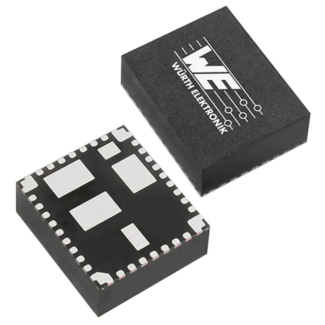
It is available in a standard industrial high power density
QFN package (11mm x 9mm x 2.8mm) with very good
thermal performance.
This module has an on-board protection circuitry to guard
against thermal overstress and electrical damage
featuring thermal shutdown, over-current, short-circuit,
overvoltage and undervoltage protections.
TYPICAL APPLICATIONS
·
·
·
·
·
·
·
Point-of-load DC-DC applications from 5V and 3.3V
rails
Industrial, test & measurement, medical applications
Communication infrastructure
System power supplies
DSPs, FPGAs, MCUs and MPU supply
I/O interface power supply
High density distributed power systems
·
·
·
·
·
·
·
·
·
·
·
·
·
·
·
·
·
·
·
·
·
·
·
·
·
·
·
Peak efficiency up to 96%
Current capability up to 4A
Input voltage range: 2.95 to 6V
Output voltage range: 0.8 to 3.6V
Continuous output power: 14.4W
Integrated shielded inductor
Low output voltage ripple: 5mV typ.
Reference accuracy over temperature: 1% max.
Adjustable switching frequency: 0.5 to 2 MHz
Current Mode control
Synchronous operation
Forced continuous mode under light load
Undervoltage lockout protection (UVLO)
Adjustable soft-start and voltage tracking
Frequency synchronization with external clock
Sequencing
Thermal shutdown
Short circuit protection
Cycle-by-cycle current limit
Output overvoltage protection
Output undervoltage and overvoltage Power Good
Pin compatible with 171020302 & 171060302
Operating ambient temperature up to 85°C
No derating within the operating temperature range
Operating junction temp. range: -40 to 125°C
UL94V-0 package material
Complies with EN55022 class B radiated emissions
standard
TYPICAL CIRCUIT DIAGRAM
we-online.com
© May 2016
Würth Elektronik eiSos GmbH & Co. KG – Data Sheet Rev. 1.0
1/48
�WPMDB1400362Q / 171040302
MagI3C Power Module
VDRM – Variable Step Down Regulator Module
PACKAGE
Top View
Bottom View
we-online.com
© May 2016
Würth Elektronik eiSos GmbH & Co. KG – Data Sheet Rev. 1.0
2/48
�WPMDB1400362Q / 171040302
MagI3C Power Module
VDRM – Variable Step Down Regulator Module
PIN DESCRIPTION
SYMBOL
NUMBER
TYPE
VIN
30,31,32
8,9,10,11,
12,13,14,
38
Power
Input Voltage. Place input capacitors as close as possible
Power
Output voltage. Place output capacitors as close as possible. For thermal
performance use copper plane(s) at these pins.
AGND
33,34
Supply
PGND
37
Power
VSENSE+
36
Input
FB
35
Input
RT/CLK
4
Input
Analog ground for internal circuitry. Connect to power ground
Power ground for the internal switching circuitry. Connect to copper plane(s) with
thermal vias for thermal performance.
Connect to positive terminal of the output capacitor. An internal resistor of 1430 Ω is
connected internally between VSENSE+ and FB. This is the upper resistor of the
feedback voltage divider.
A resistor (RSET) from FB to AGND is needed to select the output voltage. This is
the lower resistor of the feedback voltage divider.
An external resistor from RT/CLK to AGND adjusts the switching frequency of the
device. This pin can also be used to synchronize with an external clock.
INTRRT
5
Analog
Internal resistor which defines the default switching frequency.
RCOMP
1
Analog
Internal resistor of the compensation network. Must be connected to AGND.
SYMBOL
NUMBER
TYPE
UVLO
29
Input
ENABLE
28
Input
PG
27
Output
SS/TRK
6
Input
INTSS
7
Analog
DESCRIPTION
An internal undervoltage lock out resistor of 34kΩ is connected to the enable pin. If
connected to analog ground, the internal UVLO resistor divider will be activated. For
input voltages below 3.3V this pin should be left open and an optional resistor from
enable to analog ground sets the UVLO to values between 2.95 and 3.3 V.
Enable pin. Internally pull-up source. Pull to analog ground to disable. Float to
Enable.
Open drain output. The PG pin pulls low during thermal shutdown, over-current,
output overvoltage or undervoltage or disabled device. A pull-up resistor is required.
Internal current source. Connect an external capacitor to optionally increase the
soft-start time. A voltage applied to this pin allows tracking and sequencing.
An internal 3.3nF capacitor is connected to this pin. If pin 7 is connected to analog
ground, a 1.1ms soft-start time is selected.
SYMBOL
NUMBER
TYPE
COMP
3
Output
CCOMP
2
Analog
Internal capacitor of the compensation network. Do not connect.
BOOT
26
17,18,19,
20,21,22,
23,24,25,
39
Supply
Internal bootstrap pin for the high side MOSFET.
Power
Internal switch node. Do not connect these pins.
VOUT
DESCRIPTION
OPTIONAL
AUXILIARY
SWITCH
NC
we-online.com
© May 2016
15,16
DESCRIPTION
Output of the error amplifier. If an external compensation is used, pin 1 must be left
open.
Not connected to internal circuitry.
Würth Elektronik eiSos GmbH & Co. KG – Data Sheet Rev. 1.0
3/48
�WPMDB1400362Q / 171040302
MagI3C Power Module
VDRM – Variable Step Down Regulator Module
ORDERING INFORMATION
ORDER CODE
PART DESCRIPTION
SPECIFICATIONS
PACKAGE
PACKAGING UNIT
171040302
WPMDB1400362Q
4A / 14.4W version
BQFN-39
Tape and Reel, 250 pieces
178040302
Evaluation Board
4A / 14.4W version
1
PIN COMPATIBLE FAMILY MEMBERS
ORDER CODE
PART DESCRIPTION
SPECIFICATIONS
PACKAGE
PACKAGING UNIT
171020302
WPMDB1200362Q
2A / 7.2W version
BQFN-39
Tape and Reel, 250 pieces
178020302
Evaluation Board
2A / 7.2W version
171060302
WPMDB1600362Q
6A / 21.6W version
178060302
Evaluation Board
6A / 21.6W version
1
BQFN-39
Tape and Reel, 250 pieces
1
PACKAGE SPECIFICATIONS
Weight
0.54g
Molding compound
EME-G770H
UL class
UL94 V-0
Certificate number
E41429
SALES INFORMATION
SALES CONTACTS
Würth Elektronik eiSos GmbH & Co. KG
EMC & Inductive Solutions
Max-Eyth-Str. 1
74638 Waldenburg
Germany
Tel. +49 (0) 7942 945 0
www.we-online.com
powermodules@we-online.com
we-online.com
© May 2016
Würth Elektronik eiSos GmbH & Co. KG – Data Sheet Rev. 1.0
4/48
�WPMDB1400362Q / 171040302
MagI3C Power Module
VDRM – Variable Step Down Regulator Module
ABSOLUTE MAXIMUM RATINGS
Caution:
Exceeding the listed absolute maximum ratings may affect the device negatively and may cause permanent damage.
SYMBOL
LIMITS
PARAMETER
MIN
VIN
VOUT
FB
UVLO
EN
RT/CLK
PG
COMP
INTSS
MAX (1)
UNIT
Input voltage
-0.3
7
V
Output voltage
-0.6
VIN
V
Feedback voltage
-0.3
3
V
Undervoltage lockout pin voltage
-0.3
3.3
V
Enable pin Voltage
-0.3
7
V
Enable source current
RT/CLK pin voltage
RT/CLK source current
SS/TRK
(1)
SS/TRK pin voltage
-
100
µA
-0.3
6
V
-
±100
µA
-0.3
3
V
SS/TRK pin sink current
-
±100
µA
Power Good pin voltage
-0.3
7
V
Power Good sink current
-
10
mA
Output of the error amplifier pin voltage
-0.3
3
V
-
100
µA
Internal soft-start capacitor pin voltage
-0.3
3
V
COMP sink current
INTRRT
Internal resistor for the initial switching frequency pin voltage
-0.3
6
V
RCOMP
Resistor of the compensation network pin voltage
-0.3
3
V
CCOMP
Capacitor of the compensation network pin voltage
-0.3
3
V
VOUT sense pin voltage
-0.3
Vout
V
Switch node pin voltage
-0.6
7
V
10ns transient
-2
V
BOOT
Internal supply for the high MOSFET driver pin voltage
-
7
VSW
+8V
Tstorage
Assembled, non operating storage temperature
Peak case/leads temperature during reflow soldering, max. 30sec.
(JEDEC J-STD020) Maximum three cycles!
-65
150
°C
-
245±5
°C
Mechanical shock: Mil-STD-883D, Method 2002.2, 1ms, ½ sine, mounted
-
1500
G
Mechanical vibration: Mil-STD-883D, Method 2007.2, 20-2000Hz
-
20
G
VSENSE+
SW
TSOLR
we-online.com
© May 2016
V
Würth Elektronik eiSos GmbH & Co. KG – Data Sheet Rev. 1.0
5/48
�WPMDB1400362Q / 171040302
MagI3C Power Module
VDRM – Variable Step Down Regulator Module
OPERATING CONDITIONS
Operating conditions are conditions under which operation of the device is intended to be functional. All values are
referenced to GND.
MIN and MAX limits are valid for the recommended ambient temperature range of -40°C to 85°C. Typical values represents
statistically the utmost probability at following conditions: VIN = 3.3V, VOUT = 1.8V, IOUT = 4A, CIN1 = 47µF ceramic,
CIN2 = 220µF polymer electrolytic, COUT1 = 47µF ceramic, COUT2 = 100µF poly-tantalum unless otherwise noted.
SYMBOL
VIN
PARAMETER
MIN
(1)
(2)
TYP
MAX
(1)
UNIT
Input voltage
Output voltage (depending on input voltage and switching
frequency)
2.95
-
6
V
0.8
-
3.6
V
TA
Ambient temperature range
-40
-
85
TJOP
Junction temperature range
-40
-
125
°C
IOUT
Nominal output current
4
A
VOUT
(3)
°C
THERMAL SPECIFICATIONS
SYMBOL
ӨJA
ΨJT
ΨJB
TSD
we-online.com
© May 2016
PARAMETER
Junction-to-ambient thermal resistance
Junction-to-top
TYP
(4)
(5)
Junction-to-board
(6)
(2)
UNIT
12
°C/W
2.2
°C/W
9.7
°C/W
Thermal shutdown, rising
175
°C
Thermal shutdown hysteresis, falling
15
°C
Würth Elektronik eiSos GmbH & Co. KG – Data Sheet Rev. 1.0
6/48
�WPMDB1400362Q / 171040302
MagI3C Power Module
VDRM – Variable Step Down Regulator Module
ELECTRICAL SPECIFICATIONS
MIN and MAX limits are valid for the recommended ambient temperature range of -40°C to 85°C. Typical values represents
statistically the utmost probability at following conditions: VIN = 3.3V, VOUT = 1.8V, IOUT = 4A, CIN1 = 47µF ceramic,
CIN2 = 220µF polymer electrolytic, COUT1 = 47µF ceramic, COUT2 = 100µF poly-tantalum unless otherwise noted.
SYMBOL
PARAMETER
TEST CONDITIONS
MIN
(1)
TYP
(2)
MAX
(1)
UNIT
Output current
IOCP
VFB
Over current protection
Reference accuracy
Temperature variation
Line regulation
VOUT
Load regulation
-
7
-
-
-
±1
%
-40°C≤TA≤85°C, IOUT = 0A
Over VIN range, TA = 25°C,
IOUT = 0A
-
±0.3
-
%
-
±0.1
-
%
Over IOUT range, TA = 25°C
-
±0.1
-
%
-
-
±1.5
%
-
5
-
mVpp
Using RT mode
500
-
2000
kHz
RT/CLK pin open
400
500
600
kHz
Using CLK mode
500
-
2000
kHz
Accuracy
TA = 25°C, IOUT = 0A
with internal feedback resistor
Total output voltage variation
Output voltage ripple
10µF ceramic, 20MHz BW
(8)
A
(7)
Switching frequency
fSW
Switching frequency
fCLK
Synchronization clock
frequency range
Minimum CLK pulse width
75
-
-
ns
VCLK-H
RT/CLK high threshold
2.2
-
3.3
V
VCLK-L
RT/CLK low threshold
-0.3
-
0.4
V
RT/CLK to switch node delay
-
90
-
ns
PLL lock-in-time
-
14
-
µs
-
3.05
3.135
V
2.5
2.75
-
V
Enable logic high voltage
-
1.25
-
V
Enable logic low voltage
-0.3
-
1.0
V
VOUT rising, VOUT GOOD
-
93
-
%
VOUT rising, VOUT FAULT
-
107
-
%
VOUT falling, VOUT GOOD
-
105
-
%
VOUT falling, VOUT FAULT
-
91
-
%
IPG = 0.33mA
-
-
0.3
V
fCLK
VUVLO
VENABLE
Relative to AGND
Enable and undervoltage lockout
VIN increasing, UVLO pin
connected to AGND
VIN undervoltage threshold
VIN decreasing, UVLO pin
connected to AGND
Enable threshold trip point
Power Good
PG
Power Good threshold
Power Good low voltage
we-online.com
© May 2016
Würth Elektronik eiSos GmbH & Co. KG – Data Sheet Rev. 1.0
7/48
�WPMDB1400362Q / 171040302
MagI3C Power Module
VDRM – Variable Step Down Regulator Module
ELECTRICAL SPECIFICATIONS
SYMBOL
PARAMETER
TEST CONDITIONS
MIN
(1)
(2)
TYP
MAX
(1)
UNIT
Efficiency
VIN = 5V
IOUT = 2A
η
Efficiency
VIN = 3.3V
IOUT = 2A
VOUT = 3.3V, fSW = 1.0MHz
-
95
-
%
VOUT = 2.5V, fSW = 1.0MHz
-
93
-
%
VOUT = 1.8V, fSW = 1.0MHz
-
91
-
%
VOUT = 1.5V, fSW = 1.0MHz
-
89
-
%
VOUT = 1.2V, fSW = 750kHz
-
88
-
%
VOUT = 1.0V, fSW = 650kHz
-
86
-
%
VOUT = 0.8V, fSW = 650kHz
-
84
-
%
VOUT = 1.8V, fSW = 1.0MHz
-
91
-
%
VOUT = 1.5V, fSW = 1.0MHz
-
89
-
%
VOUT = 1.2V, fSW = 750kHz
-
87
-
%
VOUT = 1.0V, fSW = 650kHz
-
86
-
%
VOUT = 0.8V, fSW = 650kHz
-
83
-
%
-
µF
Input and output capacitors
CIN
External input capacitor
ceramic
Non ceramic
External output cpacitor
COUT
ceramic
Non ceramic
Output capacitor ESR
TTR
Transient Response
Transient Response
Recovery time
1A/µs load step from 1A to 3A
VOUT over/undershoot
1A/µs load step from 1A to 3A
(9)
47
47
(9)
220
(10)
150
(10)
650
µF
(11)
µF
(11)
µF
-
100
1000
-
-
25
mΩ
-
80
-
µs
-
90
-
mV
-
70
100
µA
Input quiescent current
ISD
Shutdown quiescent current
VENABLE = 0V
RELIABILITY
SYMBOL
MTBF
PARAMETER
Mean Time Between Failures
we-online.com
© May 2016
TEST CONDITIONS
Confidence level 60%,
TA=55°C, Activation energy
0.7eV, 1000 hrs test duration,
128756 samples, 0 fail
MIN
(1)
TYP
(2)
1·10
10
MAX
(1)
UNIT
h
Würth Elektronik eiSos GmbH & Co. KG – Data Sheet Rev. 1.0
8/48
�WPMDB1400362Q / 171040302
MagI3C Power Module
VDRM – Variable Step Down Regulator Module
NOTES
(1) Min and Max limits are 100% production tested at 25°C. Limits over the operating temperature range are guaranteed
through correlation using Statistical Quality Control (SQC) methods.
(2) Typical numbers are valid at 25°C ambient temperature and represent statistically the utmost probability assuming the
Gaussian distribution.
(3) Depending on heat sink design, number of PCB layers, copper thickness and air flow.
(4) Measured on a 100 x 100mm two layer board, with 35µm (1 ounce) copper, no air flow
(5) The junction-to-top characterization parameter, ΨJT, estimates the junction temperature, TJ, of a device in a real system,
using a procedure described in JESD51-2A (sections 6 and 7). TJ = ΨJT * Pdis + TT; where Pdis is the power dissipated in
the device and TT is the temperature of the top of the device.
(6) The junction-to-board characterization parameter, ΨJB, estimates the junction temperature, TJ, of a device in a real
system, using a procedure described in JESD51-2A (sections 6 and 7). T J = ΨJB * Pdis + TB; where Pdis is the power
dissipated in the device and TB is the temperature of the board 1mm from the device.
(7) The stated limit of the set-point voltage tolerance includes the tolerance of both the internal voltage reference and the
internal adjustment resistor. The overall output voltage tolerance is affected by the tolerance of the external R SET
resistor.
(8) The industry standard for comparison of the output voltage ripple between switching regulators or modules requires a
10µF ceramic (sometimes additional 1µF ceramic in parallel) at the point of load where the voltage measurement is
done using an oscilloscope with its probe and probe jack for low voltage/high frequency (low impedance) measurement.
The oscilloscopes bandwidth is limited at 20MHz.
(9) A minimum of 47µF of ceramic capacitance is required across the input for proper operation. Locate the capacitor
directly at VIN of the device. An additional 220µF of bulk capacitance is recommended.
(10) The amount of required output capacitance varies depending on the output voltage. The amount of required
capacitance must include at least 47µF of ceramic capacitance. Locate the capacitance close to the device. Adding
additional capacitance close to the load improves the response of the regulator to load transients.
(11) When using both ceramic and non-ceramic output capacitance, the combined maximum must not exceed 1200µF.
we-online.com
© May 2016
Würth Elektronik eiSos GmbH & Co. KG – Data Sheet Rev. 1.0
9/48
�WPMDB1400362Q / 171040302
MagI3C Power Module
VDRM – Variable Step Down Regulator Module
TYPICAL PERFORMANCE CURVES
If not otherwise specified, the following conditions apply: VIN = 3.3V - 5V; CIN = 2 x 47µF X7R ceramic; COUT = 2x 47µF X7R
ceramic, TAMB = 25°C.
RADIATED EMISSIONS EN55022 (CISPR-22) CLASS B COMPLIANT
Measured on module with PCB and without external filters at 3m antenna distance
70
Radiated Emissions 171040302
VIN = 5V, VOUT = 1.8V, fSW = 1MHz, ILOAD = 4A
Radiated Emissions [dBµV/m]
60
Horizontal
Vertical
50
EN55022 Class A
40
EN55022 Class B
30
20
10
0
30
100
1000
Frequency [MHz]
70
Radiated Emissions 171040302
VIN = 3.3V, VOUT = 1.8V, fSW = 1MHz, I LOAD = 4A
Radiated Emissions [dBµV/m]
60
Horizontal
Vertical
50
EN55022 Class A
40
EN55022 Class B
30
20
10
0
30
100
1000
Frequency [MHz]
we-online.com
© May 2016
Würth Elektronik eiSos GmbH & Co. KG – Data Sheet Rev. 1.0
10/48
�WPMDB1400362Q / 171040302
MagI3C Power Module
VDRM – Variable Step Down Regulator Module
EFFICIENCY
171040302 5V Input
100
95
90
Efficiency [%]
85
80
Vout = 3.3V, fsw = 1MHz
75
Vout = 2.5V, fsw = 1MHz
70
Vout = 1.8V, fsw = 1MHz
65
Vout = 1.2V, fsw = 750kHz
60
Vout = 0.8V, fsw = 650kHz
55
50
0
0,5
1
1,5
2
2,5
Output Current [A]
3
3,5
4
171040302 3.3V Input
100
95
90
Efficiency [%]
85
80
Vout = 2.5V, fsw = 1MHz
75
Vout = 1.8V, fsw = 1MHz
70
Vout = 1.2V, fsw = 750kHz
65
Vout = 0.8V, fsw = 650kHz
60
55
50
0
we-online.com
© May 2016
0,5
1
1,5
2
2,5
Output Current [A]
3
3,5
4
Würth Elektronik eiSos GmbH & Co. KG – Data Sheet Rev. 1.0
11/48
�WPMDB1400362Q / 171040302
MagI3C Power Module
VDRM – Variable Step Down Regulator Module
POWER DISSIPATION
171040302 5V Input
1,40
Power Dissipation [W]
1,20
1,00
Vout = 3.3V, fsw = 1MHz
0,80
Vout = 2.5V, fsw = 1MHz
0,60
Vout = 1.8V, fsw = 1MHz
0,40
Vout = 1.2V, fsw = 750kHz
Vout = 0.8V, fsw = 650kHz
0,20
0,00
0
0,5
1
1,5
2
2,5
Output Current [A]
3
3,5
4
171040302 3.3V Input
1,40
Power Dissipation [W]
1,20
1,00
0,80
Vout = 2.5V, fsw = 1MHz
0,60
Vout = 1.8V, fsw = 1MHz
Vout = 1.2V, fsw = 750kHz
0,40
Vout = 0.8V, fsw = 650kHz
0,20
0,00
0
we-online.com
© May 2016
0,5
1
1,5
2
2,5
Output Current [A]
3
3,5
4
Würth Elektronik eiSos GmbH & Co. KG – Data Sheet Rev. 1.0
12/48
�WPMDB1400362Q / 171040302
MagI3C Power Module
VDRM – Variable Step Down Regulator Module
OUTPUT POWER DERATING
171040302 Derating (all output voltages)
5
4,5
Output Current [A]
4
3,5
3
2,5
2
1,5
1
0,5
0
20 25 30 35 40 45 50 55 60 65 70 75 80 85
Ambient Temperature [°C]
Note : see TA limits in operating conditions on page 6.
we-online.com
© May 2016
Würth Elektronik eiSos GmbH & Co. KG – Data Sheet Rev. 1.0
13/48
�WPMDB1400362Q / 171040302
MagI3C Power Module
VDRM – Variable Step Down Regulator Module
OUTPUT VOLTAGE RIPPLE
171040302 5V Input
Output Voltage Ripple [mVpp]
7
6
5
Vout = 3.3V, fsw = 1.5MHz
4
Vout = 2.5V, fsw = 1.5MHz
3
Vout = 1.8V, fsw = 1MHz
2
Vout = 1.2V, fsw = 750kHz
Vout = 0.8V, fsw = 650kHz
1
0
0
0,5
1
1,5
2
2,5
Output Current [A]
3
3,5
4
171040302 3.3V Input
Output Voltage Ripple [mVpp]
7
6
5
4
Vout = 2.5V, fsw = 1MHz
Vout = 1.8V, fsw = 1MHz
3
Vout = 1.2V, fsw = 750kHz
2
Vout = 0.8V, fsw = 650kHz
1
0
0
we-online.com
© May 2016
0,5
1
1,5
2
2,5
Output Current [A]
3
3,5
4
Würth Elektronik eiSos GmbH & Co. KG – Data Sheet Rev. 1.0
14/48
�WPMDB1400362Q / 171040302
MagI3C Power Module
VDRM – Variable Step Down Regulator Module
LIGHT LOAD OPERATION
The 171040302 forces the CCM (Continuous Conduction Mode) operation at light load (forced CCM). The inductor current
during tOFF can flow in the opposite direction, i.e. from the output capacitor and load to ground, through the low side
MOSFET. In this way during tOFF the output capacitor is discharged and loses the excess of charge gathered during t ON.
In this way the switching frequency always remains constant, giving a relevant advantage in terms of filtering and avoiding
interferences in undesired frequency ranges. Any load change will simply shift the inductor current up and down (see figure
below).
we-online.com
© May 2016
Würth Elektronik eiSos GmbH & Co. KG – Data Sheet Rev. 1.0
15/48
�WPMDB1400362Q / 171040302
MagI3C Power Module
VDRM – Variable Step Down Regulator Module
OUTPUT VOLTAGE RIPPLE AT LIGHT LOAD
In addition, the forced CCM implemented by the 171040302 keeps the output voltage ripple constant and low at all
conditions (see figure below).
we-online.com
© May 2016
Würth Elektronik eiSos GmbH & Co. KG – Data Sheet Rev. 1.0
16/48
�WPMDB1400362Q / 171040302
MagI3C Power Module
VDRM – Variable Step Down Regulator Module
BLOCK DIAGRAM
26
17-25, 39
BOOT
Power Module
SW
1µH
VIN
V IN
CIN
100n
28
27
8-14, 38
V OUT
36
C OUT
1430Ω
PWM Contr oller/
Dr iver/
Prote ction Circuitry
ENABLE
34k
29
VSENSE+
C boot
48.7k
VOUT
E rror A mpli fier
35
FB
UVLO
0.8V
R SET
VRE F
PG
5
2
COMP
37 1
CC OMP
33,
34
RC OMP
RT/CLK
4
PGND
6
AGND
7
INTRRT
INTSS
SS/TR K
Current
Source
3
CIRCUIT DESCRIPTION
The MagI³C Power Module series 1710x0302 is based on a synchronous step down regulator with integrated MOSFETs and
a power inductor. The control scheme is based on a Current Mode (CM) regulation loop.
The VOUT of the regulator is divided with the feedback resistor network of internal 1430Ω and external R SET and fed into the
FB pin. The error amplifier compares this signal with the internal 0.803V reference. The error signal is amplified and controls
the on-time of a fixed frequency pulse width generator. This signal drives the power MOSFETs.
The Current Mode architecture features a constant frequency during load steps. Only the on-time is modulated. It is
internally compensated and stable with low ESR output capacitors and requires no external compensation network.
This architecture supports fast transient response and very small output ripple values (less than 10mV) are achieved.
we-online.com
© May 2016
Würth Elektronik eiSos GmbH & Co. KG – Data Sheet Rev. 1.0
17/48
�WPMDB1400362Q / 171040302
MagI3C Power Module
VDRM – Variable Step Down Regulator Module
DESIGN FLOW
The next 10 simple steps will show how to select the external components to design your power application.
Essential Steps
1.
2.
3.
4.
Set output voltage
Set operating frequency
Select input capacitor
Select output capacitor
Optional Steps
5.
6.
7.
8.
9.
10.
Select soft-start capacitor
Select undervoltage lockout divider
Enable / Disable
Voltage tracking
Synchronization to an external clock
Power Good
we-online.com
© May 2016
Würth Elektronik eiSos GmbH & Co. KG – Data Sheet Rev. 1.0
18/48
�WPMDB1400362Q / 171040302
MagI3C Power Module
VDRM – Variable Step Down Regulator Module
Step 1 Setting the output voltage (VOUT )
The output voltage is selected with a resistor divider across FB pin and AGND. The upper resistor of 1430 Ω of the feedback
voltage resistor divider is located inside the module. The output voltage adjustment range is from 0.8V to 3.6V.
R
VREF is the internal reference voltage (0.8V).
=
V
V
∗ 1430Ω
(Ω) (1)
−V
VOUT
3.3V
3.0V
2.5V
1.8V
1.5V
1.2V
1.0V
0.8V
RSET (E96)
453Ω
523Ω
665Ω
1130Ω
1620Ω
2870Ω
5620Ω
open
VOUT 36
VOUT
143 0Ω
35
AGND
FB
we-online.com
© May 2016
RSET
Würth Elektronik eiSos GmbH & Co. KG – Data Sheet Rev. 1.0
19/48
�WPMDB1400362Q / 171040302
MagI3C Power Module
VDRM – Variable Step Down Regulator Module
Step 2 Setting the operating frequency (fSW)
The switching frequency must be selected according to the input voltage, output voltage and load current for the best
performance in loop regulation and transient response.
Note: RRT open (fSW = 500 kHz) is only allowed under specific conditions (see table below)!
VIN = 5V
OPERATING
FREQUENCY
[kHz]
RRT [kΩ]
VIN = 3.3V
IOUT = 0 to 1.5A
IOUT > 1.5A
IOUT = 0 to 2A
VOUT RANGE [V]
VOUT RANGE [V]
VOUT RANGE [V]
MIN
MAX
MIN
MAX
MIN
MAX
500
open
0.8
1.4
0.8
1.0
0.8
2.2
550
3400
0.8
1.6
0.8
1.1
0.8
2.4
600
1800
0.8
1.8
0.8
1.2
0.8
2.5
650
1200
0.8
2.1
0.8
1.4
0.8
2.5
700
887
0.8
2.6
0.8
1.6
0.8
2.5
750
715
0.9
3.6
0.9
1.8
0.8
2.5
800
590
0.9
3.6
0.9
2.1
0.8
2.5
900
511
1.0
3.6
1.0
3.6
0.8
2.5
1000
348
1.2
3.6
1.2
3.6
0.8
2.5
1250
232
1.4
3.6
1.4
3.6
1.0
2.4
1500
174
1.7
3.6
1.7
3.6
1.1
2.3
1750
137
2.0
3.6
2.0
3.6
1.3
2.2
2000
113
2.3
3.4
2.3
3.3
1.5
2.2
we-online.com
© May 2016
Würth Elektronik eiSos GmbH & Co. KG – Data Sheet Rev. 1.0
20/48
�WPMDB1400362Q / 171040302
MagI3C Power Module
VDRM – Variable Step Down Regulator Module
Step 3 Select input capacitor (CIN)
The energy at the input of the power module is stored in the input capacitor. A small input capacitor (100nF) is integrated
inside the 1710x0302 MagI³C Power Module series, ensuring good EMI performance. Additional input capacitance is
required external to the power module to provide cycle-by-cycle switch current and to support load transients. The external
input capacitors must be placed directly at VIN pin. The input capacitor can be several capacitors in parallel. Input capacitor
selection is generally directed to satisfy the input ripple current requirements rather than by capacitance value. Input ripple
current rating is dictated by the equation:
I
1
≈ ∗ I
2
∗
D
V
(2) where D ≈
1−D
V
As a point of reference, the worst case ripple current will occur when the module is presented with full load current and when
VIN = 2 x VOUT.
Recommended minimum input capacitance is 47µF X7R or X5R ceramic with a voltage rating at least 25% higher than the
maximum applied input voltage for the application. It is also recommended that attention be paid to the voltage and
temperature deratings of the capacitor selected. It should be noted that ripple current rating of ceramic capacitors may be
missing from the capacitor data sheet and you may have to contact the capacitor manufacturer for this rating.
If the system design requires a certain minimum value of peak-to-peak input ripple voltage (ΔV IN) then the following equation
may be used:
C
≥
I
∗ D ∗ (1 − D)
V
(3) where D ≈
f
∗ ∆V
V
CCM = continuous conduction mode
Additional bulk capacitance with higher ESR may be required to damp any resonant effects of the input capacitance and
parasitic inductance of the incoming supply lines.
we-online.com
© May 2016
Würth Elektronik eiSos GmbH & Co. KG – Data Sheet Rev. 1.0
21/48
�WPMDB1400362Q / 171040302
MagI3C Power Module
VDRM – Variable Step Down Regulator Module
Step 4 Select output capacitor (COUT )
L
HS Mosfet
IL
Iout
VCOUT
COUT
CIN
VIN
LS Mosfet
VOUT
Rload
ESR
VES R
None of the required output capacitors are integrated within the module. The output capacitor must meet the worst case
RMS current rating of 0.5 ∗ ∆ , as calculated in equation (4).
∆I =
V
∗ (V − V
f ∗L∗V
)
(4)
Selection by output voltage ripple requirements
The capacitor should be selected in order to minimize the output voltage and provide a stable voltage at the output.
Under steady state conditions, the voltage ripple observed at the output can be defined as:
V
= ∆I ∗ ESR + ∆I ∗
1
8∙f ∙C
(5)
Very low ESR capacitors, like ceramic and polymer electrolytic, are recommended. If a low ESR capacitor is selected,
equation (4) can be simplified and a first condition for the minimum capacitance value can be derived:
C
≥
8∗V
∆I
∗f
(6)
Beyond that, additional capacitance will reduce output ripple as long as the ESR is low enough to permit it. Please consider
the derating of the nominal capacitance value due to temperature, aging and applied DC voltage (only for MLCC, e.g. X7R
up to -50%).
we-online.com
© May 2016
Würth Elektronik eiSos GmbH & Co. KG – Data Sheet Rev. 1.0
22/48
�WPMDB1400362Q / 171040302
MagI3C Power Module
VDRM – Variable Step Down Regulator Module
The use of very low ESR capacitors leads to an output voltage ripple as shown below:
Output voltage ripple with low ESR capacitors
Output voltage ripple [mV]
10
5
0
-5
-10
0
1
2
3
time [µs]
When capacitors with slightly higher ESR are utilized, the dominant parameter which influences the output voltage ripple is
just the ESR:
ESR ≤
V
∆I
(7)
Consequently the shape of the output voltage ripple changes, as shown below:
Output voltage ripple with high ESR capacitors
Output voltage ripple [mV]
100
50
0
-50
-100
0
1
2
3
time [µs]
we-online.com
© May 2016
Würth Elektronik eiSos GmbH & Co. KG – Data Sheet Rev. 1.0
23/48
�WPMDB1400362Q / 171040302
MagI3C Power Module
VDRM – Variable Step Down Regulator Module
Selection by load step requirements
The output voltage is also affected by load transients (see picture below).
When the output current transitions from a low to a high value, the voltage at the output capacitor (V OUT) drops. This involves
two contributing factors. One is caused by the voltage drop across the ESR (V ESR) and depends on the slope of the rising
edge of the current step (t rise). For low ESR values and small load currents, this is often negligible. It can be calculated as
follows:
V
Where ∆
= ESR ∗ ∆I
(8)
is the load step, as shown in the picture below (simplified: no voltage ripple is shown).
IOUT
∆IOUT
0
trise
t
VOUT
VESR
∆VOUT
Vdischarge
0
t
td
treg
The second contributing factor is the voltage drop due to discharge of the output capacitor, which can be estimated as:
V
=
∆I
∙t
(9)
2∙C
In a current mode architecture the t d is strictly related to the bandwidth of the regulation loop and influenced by the COUT
(increasing COUT, the td increases as well).
we-online.com
© May 2016
Würth Elektronik eiSos GmbH & Co. KG – Data Sheet Rev. 1.0
24/48
�WPMDB1400362Q / 171040302
MagI3C Power Module
VDRM – Variable Step Down Regulator Module
In order to choose the value of the output capacitor, the following steps should be utilized:
1.
2.
3.
According to the operating conditions (VIN, VOUT and fSW ), select the minimum COUT recommended in table on
page 35.
Measure td.
Calculate the appropriate value of COUT for the maximum voltage drop Vdischarge allowed at a defined load step,
using the following equation (10), derived from equation (9):
C
4.
≥
∆I
2∙V
∙t
(10)
As above mentioned, changing COUT affects also td. Therefore a new measurement should be performed and, if
necessary, step 2 and 3 repeated (it is an iterative process and few steps could be required).
Example. VIN = 5V, VOUT = 3.3V, ΔIOUT = 2.5A, fsw = 1.5MHz, ΔVOUT