52
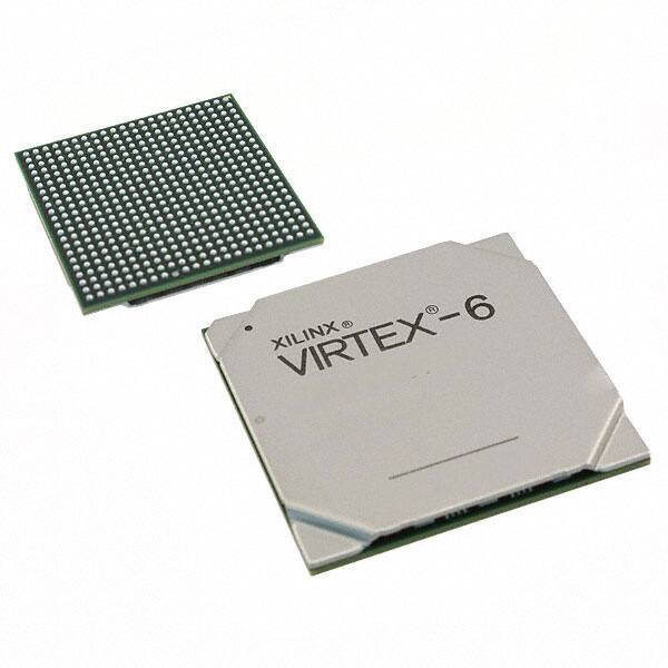
Virtex-6 CXT Family Data Sheet
DS153 (v1.6) February 11, 2011
Product Specification
General Description
Virtex®-6 CXT FPGAs provide designers needing power-optimized 3.75 Gb/s transceiver performance with an optimized
ratio of built-in system-level blocks. These include 36 Kb block RAM/FIFOs, up to 15 Mb of block RAM, up to 768 DSP48E1
slices, enhanced mixed-mode clock management blocks, PCI Express® (GEN 1) compatible integrated blocks, a tri-mode
Ethernet media access controller (MAC), up to 241K logic cells, and strong IP support. Using the third generation ASMBL™
(Advanced Silicon Modular Block) column-based architecture, the Virtex-6 CXT family also contains SelectIO™ technology
with built-in digitally controlled impedance, ChipSync™ source-synchronous interface blocks, enhanced mixed-mode clock
management blocks, and advanced configuration options. Customers needing higher transceiver speeds, greater I/O
performance, additional Ethernet MACs, or greater capacity should instead use the Virtex-6 LXT or SXT families. Built on a
40 nm state-of-the-art copper process technology, Virtex-6 CXT FPGAs are a programmable alternative to custom ASIC
technology. Virtex-6 CXT FPGAs are the programmable silicon foundation for Targeted Design Platforms that deliver
integrated software and hardware components to enable designers to focus on innovation as soon as their development
cycle begins.
Summary of Virtex-6 CXT FPGA Features
•
•
•
•
Advanced, high-performance, FPGA Logic
•
Real 6-input look-up table (LUT) technology
•
Dual LUT5 (5-input LUT) option
•
LUT/dual flip-flop pair for applications requiring rich
register mix
•
Improved routing efficiency
•
64-bit (or 32 x 2-bit) distributed LUT RAM option
•
SRL32/dual SRL16 with registered outputs option
Powerful mixed-mode clock managers (MMCM)
•
MMCM blocks provide zero-delay buffering, frequency
synthesis, clock-phase shifting, input-jitter filtering, and
phase-matched clock division
36-Kb block RAM/FIFOs
•
Dual-port RAM blocks
•
Programmable
Dual-port widths up to 36 bits
Simple dual-port widths up to 72 bits
•
Enhanced programmable FIFO logic
•
Built-in optional error-correction circuitry
•
Optionally use each block as two independent 18 Kb
blocks
High-performance parallel SelectIO technology
•
1.2 to 2.5V I/O operation
•
Source-synchronous interfacing using
ChipSync™ technology
•
Digitally controlled impedance (DCI) active termination
•
Flexible fine-grained I/O banking
•
High-speed memory interface support with integrated
write-leveling capability
•
•
•
•
•
•
•
•
•
•
•
Advanced DSP48E1 slices
•
25 x 18, two's complement multiplier/accumulator
•
Optional pipelining
•
New optional pre-adder to assist filtering applications
•
Optional bitwise logic functionality
•
Dedicated cascade connections
Flexible configuration options
•
SPI and Parallel Flash interface
•
Multi-bitstream support with dedicated fallback
reconfiguration logic
•
Automatic bus width detection
Integrated interface blocks for PCI Express designs
•
Compliant to the PCI Express Base Specification 2.0
•
Gen1 Endpoint (2.5 Gb/s) support with GTX transceivers
•
x1, x2, x4, or x8 lane support per block
•
One virtual channel, eight traffic classes
GTX transceivers: 150 Mb/s to 3.75 Gb/s
Integrated 10/100/1000 Mb/s Ethernet MAC block
•
Supports 1000BASE-X PCS/PMA and SGMII using
GTX transceivers
•
Supports MII, GMII, and RGMII using SelectIO
technology resources
40 nm copper CMOS process technology
1.0V core voltage
Two speed grades (-1 and -2)
Two temperature grades (commercial and industrial)
High signal-integrity flip-chip packaging available in standard
or Pb-free package options
Compatibility across sub-families: CXT, LXT, and SXT
devices are footprint compatible in the same package
© 2009–2011 Xilinx, Inc. XILINX, the Xilinx logo, Virtex, Spartan, ISE, and other designated brands included herein are trademarks of Xilinx in the United States and other
countries. All other trademarks are the property of their respective owners.
DS153 (v1.6) February 11, 2011
Product Specification
www.xilinx.com
1
�Virtex-6 CXT Family Data Sheet
Virtex-6 CXT FPGA Feature Summary
Table 1: Virtex-6 CXT FPGA Feature Summary by Device
Configurable Logic
Blocks (CLBs)
Logic
Cells
Device
Slices(1)
Max
Distributed
RAM (Kb)
Block RAM Blocks
DSP48E1
Slices(2)
MMCMs(4)
Interface
Maximum
Ethernet
Blocks for
GTX
MACs(5)
PCI Express
Transceivers
Total
I/O
Banks(6)
Max
User
I/O(7)
18 Kb(3)
36 Kb
Max (Kb)
5,616
6
1
1
12
9
360
XC6VCX75T
74,496
11,640
1,045
288
312
156
XC6VCX130T
128,000
20,000
1,740
480
528
264
9,504
10
2
1
16
15
600
XC6VCX195T
199,680
31,200
3,040
640
688
344
12,384
10
2
1
16
15
600
XC6VCX240T
241,152
37,680
3,650
768
832
416
14,976
12
2
1
16
18
600
Notes:
1.
2.
3.
4.
5.
6.
7.
Each Virtex-6 CXT FPGA slice contains four LUTs and eight flip-flops, only some slices can use their LUTs as distributed RAM or SRLs.
Each DSP48E1 slice contains a 25 x 18 multiplier, an adder, and an accumulator.
Block RAMs are fundamentally 36 Kbits in size. Each block can also be used as two independent 18 Kb blocks.
Each CMT contains two mixed-mode clock managers (MMCM).
This table lists individual Ethernet MACs per device.
Does not include configuration Bank 0.
This number does not include GTX transceivers.
Virtex-6 CXT FPGA Device-Package Combinations and Maximum I/Os
Virtex-6 CXT FPGA package combinations with the maximum available I/Os per package are shown in Table 2.
Table 2: Virtex-6 CXT FPGA Device-Package Combinations and Maximum Available I/Os
Package
FF484
FFG484
FF784
FFG784
FF1156
FFG1156
Size (mm)
23 x 23
29 x 29
35 x 35
Device
GTs
I/O
GTs
I/O
XC6VCX75T
8 GTXs
240
12 GTXs
360
XC6VCX130T
8 GTXs
240
GTs
I/O
12 GTXs
400
16 GTXs
600
XC6VCX195T
12 GTXs
400
16 GTXs
600
XC6VCX240T
12 GTXs
400
16 GTXs
600
Notes:
1.
Flip-chip packages are also available in Pb-Free versions (FFG).
Virtex-6 CXT FPGA Ordering Information
The Virtex-6 CXT FPGA ordering information shown in Figure 1 applies to all packages including Pb-Free.
X-Ref Target - Figure 1
Example: XC6VCX240T-1FFG1156C
Device Type
Speed Grade
(-1, -2)
Temperature Range:
C = Commercial (TJ = 0°C to +85°C)
I = Industrial (TJ = –40°C to +100°C)
Number of Pins
Pb-Free
Package Type
DS153_01_062109
Figure 1: Virtex-6 CXT FPGA Ordering Information
DS153 (v1.6) February 11, 2011
Product Specification
www.xilinx.com
2
�Virtex-6 CXT Family Data Sheet
Virtex-6 CXT FPGA Documentation
In addition to the data sheet information found herein, complete and up-to-date documentation of the Virtex-6 family of
FPGAs is available on the Xilinx website and available for download:
Virtex-6 FPGA Configuration Guide (UG360)
Virtex-6 FPGA GTX Transceivers User Guide (UG366)
This all-encompassing configuration guide includes
chapters on configuration interfaces (serial and parallel),
multi-bitstream management, bitstream encryption,
boundary-scan and JTAG configuration, and reconfiguration
techniques.
This guide describes the GTX transceivers available in all
the Virtex-6 CXT FPGAs.
Virtex-6 FPGA SelectIO Resources User Guide (UG361)
This guide describes the SelectIO™ resources available in
all the Virtex-6 CXT devices.
Virtex-6 FPGA Clocking Resources User Guide (UG362)
This guide describes the clocking resources available in all
the Virtex-6 CXT devices, including the MMCM and clock
buffers.
Virtex-6 FPGA Tri-Mode Ethernet MAC User Guide
(UG368)
This guide describes the dedicated tri-mode Ethernet
media access controller (TEMAC) available in all the
Virtex-6 CXT FPGAs.
Virtex-6 FPGA Data Sheet: DC and Switching
Characteristics (DS152)
Reference this data sheet when considering device
migration to the Virtex-6 LXT and SXT families. It contains
the DC and Switching Characteristic specifications
specifically for the Virtex-6 LXT and SXT families.
Virtex-6 FPGA Memory Resources User Guide (UG363)
This guide describes the Virtex-6 CXT device block RAM
and FIFO capabilities.
Virtex-6 FPGA CLB User Guide (UG364)
This guide describes the capabilities of the configurable
logic blocks (CLB) available in all Virtex-6 CXT devices.
Virtex-6 FPGA DSP48E1 Slice User Guide (UG369)
Virtex-6 FPGA Packaging and Pinout Specifications
(UG365)
These specifications includes the tables for device/package
combinations and maximum I/Os, pin definitions, pinout
tables, pinout diagrams, mechanical drawings, and thermal
specifications of the Virtex-6 LXT and SXT families.
Reference these specifications when considering device
migration to the Virtex-6 LXT and SXT families.
This guide describes the architecture of the DSP48E1 slice
in Virtex-6 CXT FPGAs and provides configuration
examples.
Configuration Bitstream Overview for CXT Devices
This section contains two tables similar to those in the Virtex-6 FPGA Configuration Guide only updated for the CXT family.
The Virtex-6 CXT FPGA bitstream contains commands to the FPGA configuration logic as well as configuration data.
Table 3 gives a typical bitstream length and Table 4 gives the specific device ID codes for the Virtex-6 CXT devices.
Table 3: Virtex-6 CXT FPGA Bitstream Length
Device
Table 4: Virtex-6 CXT FPGA Device ID Codes
Total Number of Configuration Bits
Device
ID Code (Hex)
XC6VCX75T
26,239,328
XC6VCX75T
0x042C4093
XC6VCX130T
43,719,776
XC6VCX130T
0x042CA093
XC6VCX195T
61,552,736
XC6VCX195T
0x042CC093
XC6VCX240T
73,859,552
XC6VCX240T
0x042D0093
DS153 (v1.6) February 11, 2011
Product Specification
www.xilinx.com
3
�Virtex-6 CXT Family Data Sheet
CLB Overview for CXT Devices
Table 5, updated specifically for the CXT family from a similar table in the Virtex-6 FPGA CLB User Guide, shows the
available resources in all Virtex-6 CXT FPGA CLBs.
Table 5: Virtex-6 CXT FPGA Logic Resources Available in All CLBs
Device
Total
Slices
SLICELs SLICEMs
Number of
6-Input LUTs
Maximum
Distributed RAM (Kb)
Shift
Register (Kb)
Number of
Flip-Flops
XC6VCX75T
11,640
7,460
4,180
46,560
1045
522.5
93,120
XC6VCX130T
20,000
13,040
6,960
80,000
1740
870
160,000
XC6VCX195T
31,200
19,040
12,160
124,800
3140
1570
249,600
XC6VCX240T
37,680
23,080
14,600
150,720
3770
1885
301,440
Regional Clock Management for CXT Devices
Table 6, updated from the Virtex-6 FPGA Clocking Resources User Guide specifically for the CXT family, shows the number
of clock regions in all Virtex-6 CXT FPGA CLBs.
Table 6: Virtex-6 CXT FPGA Clock Regions
Device
Number of Clock Regions
XC6VCX75T
6
XC6VCX130T
10
XC6VCX195T
10
XC6VCX240T
12
CXT Packaging Specifications
Table 7, updated from the Virtex-6 FPGA Packaging and Pinout Specifications specifically for the CXT family, shows the
number of GTX transceiver I/O channels. Table 8 shows the number of available I/Os and the number of differential I/O pairs
for each Virtex-6 device/package combination.
Table 7: Number of Serial Transceivers (GTs) I/O Channels/Device
I/O
Channels
Device
CX75T(1)
CX130T(2)
CX195T(3)
CX240T(4)
MGTRXP
8 or 12
8, 12, or 16
12 or 16
12 or 16
MGTRXN
8 or 12
8, 12, or 16
12 or 16
12 or 16
MGTTXP
8 or 12
8, 12, or 16
12 or 16
12 or 16
MGTTXN
8 or 12
8, 12, or 16
12 or 16
12 or 16
Notes:
1.
2.
3.
4.
The XC6VCX75T has 8 GTX I/O channels in the FF484/FFG484 package and 12 GTX I/O channels in the FF784/FFG784 package.
The XC6VCX130T has 8 GTX I/O channels in the FF484/FFG484 package, 12 GTX I/O channels in the FF784/FFG784 package, and 16
GTX I/O channels in the FF1156/FFG1156 package.
The XC6VCX195T has 12 GTX I/O channels in the FF784/FFG784 package and 16 GTX I/O channels in the FF1156/FFG1156 package.
The XC6VCX240T has 12 GTX I/O channels in the FF784/FFG784 package and 16 GTX I/O channels in the FF1156/FFG1156 package.
DS153 (v1.6) February 11, 2011
Product Specification
www.xilinx.com
4
�Virtex-6 CXT Family Data Sheet
Table 8: Available I/O Pin/Device/Package Combinations
Virtex-6 CXT FPGA Package
Virtex-6 CXT Device
User I/O Pins
FF484
FF784
FF1156
Available User I/Os
240
360
–
Differential I/O Pairs
120
180
–
Available User I/Os
240
400
600
Differential I/O Pairs
120
200
300
Available User I/Os
–
400
600
Differential I/O Pairs
–
200
300
Available User I/Os
–
400
600
Differential I/O Pairs
–
200
300
XC6VCX75T
XC6VCX130T
XC6VCX195T
XC6VCX240T
GTX Transceivers in CXT Devices
CXT devices have between 8 to 16 gigabit transceiver circuits. Each GTX transceiver is a combined transmitter and receiver
capable of operating at a data rate between 480 Mb/s and 3.75 Gb/s. Lower data rates can be achieved using FPGA logicbased oversampling. The transmitter and receiver are independent circuits that use separate PLLs to multiply the reference
frequency input by certain programmable numbers between 2 and 25, to become the bit-serial data clock. Each GTX
transceiver has a large number of user-definable features and parameters. All of these can be defined during device
configuration, and many can also be modified during operation.
DS153 (v1.6) February 11, 2011
Product Specification
www.xilinx.com
5
�Virtex-6 CXT Family Data Sheet
FF484 Package Placement Diagrams
Figure 2 and Figure 3 show the placement diagrams for the GTX transceivers in the FF484 package.
Note: Unbonded locations in the FF484 package are:
•
CX75T: X0Y8, X0Y9, X0Y10, X0Y11
•
CX130T: X0Y0, X0Y1, X0Y2, X0Y3, and X0Y12, X0Y13, X0Y14, X0Y15
X-Ref Target - Figure 2
X-Ref Target - Figure 3
B1
MGTRXP3_115
W3
MGTRXP3_114
B2
MGTRXN3_115
W4
MGTRXN3_114
CX75T: GTXE1_X0Y3
CX130T: GTXE1_X0Y7
CX75T: GTXE1_X0Y7
CX130T: GTXE1_X0Y11
D1
MGTTXP3_115
M1
MGTTXP3_114
D2
MGTTXN3_115
M2
MGTTXN3_114
C3
MGTRXP2_115
Y1
MGTRXP2_114
C4
MGTRXN2_115
Y2
MGTRXN2_114
CX75T: GTXE1_X0Y2
CX130T: GTXE1_X0Y6
CX75T: GTXE1_X0Y6
CX130T: GTXE1_X0Y10
F1
MGTTXP2_115
P1
MGTTXP2_114
F2
MGTTXN2_115
P2
MGTTXN2_114
J4
MGTREFCLK1P_115
R4
MGTREFCLK1P_114
J3
MGTREFCLK1N_115
R3
MGTREFCLK1N_114
L4
MGTREFCLK0P_115
U4
MGTREFCLK0P_114
L3
MGTREFCLK0N_115
U3
MGTREFCLK0N_114
E3
MGTRXP1_115
AA3
MGTRXP1_114
E4
MGTRXN1_115
AA4
MGTRXN1_114
QUAD_115
QUAD_114
CX75T: GTXE1_X0Y1
CX130T: GTXE1_X0Y5
CX75T: GTXE1_X0Y5
CX130T: GTXE1_X0Y9
H1
MGTTXP1_115
T1
MGTTXP1_114
H2
MGTTXN1_115
T2
MGTTXN1_114
G3
MGTRXP0_115
AB1
MGTRXP0_114
G4
MGTRXN0_115
AB2
MGTRXN0_114
CX75T: GTXE1_X0Y0
CX130T: GTXE1_X0Y4
CX75T: GTXE1_X0Y4
CX130T: GTXE1_X0Y8
K1
MGTTXP0_115
V1
MGTTXP0_114
K2
MGTTXN0_115
V2
MGTTXN0_114
ds153_03_041510
ds153_02_041510
Figure 2: Placement Diagram for the FF484 Package
(1 of 2)
DS153 (v1.6) February 11, 2011
Product Specification
Figure 3: Placement Diagram for the FF484 Package
(2 of 2)
www.xilinx.com
6
�Virtex-6 CXT Family Data Sheet
FF784 Package Placement Diagrams
Figure 4 through Figure 6 show the placement diagrams for the GTX transceivers in the FF784 package.
Note: Unbonded locations in the FF784 package are:
•
CX130T: X0Y0, X0Y1, X0Y2, X0Y3
•
CX195T: X0Y0, X0Y1, X0Y2, X0Y3
•
CX240T: X0Y0, X0Y1, X0Y2, X0Y3
X-Ref Target - Figure 4
X-Ref Target - Figure 5
CX75T: GTXE1_X0Y11
CX130T: GTXE1_X0Y15
CX195T: GTXE1_X0Y15
CX240T: GTXE1_X0Y15
CX75T: GTXE1_X0Y10
CX130T: GTXE1_X0Y14
CX195T: GTXE1_X0Y14
CX240T: GTXE1_X0Y14
A3
MGTRXP3_116
A4
MGTRXN3_116
D1
MGTTXP3_116
D2
MGTTXN3_116
B1
MGTRXP2_116
B2
MGTRXN2_116
F1
MGTTXP2_116
F2
MGTTXN2_116
G4
G3
CX75T: GTXE1_X0Y7
CX130T: GTXE1_X0Y11
CX195T: GTXE1_X0Y11
CX240T: GTXE1_X0Y11
CX75T: GTXE1_X0Y8
CX130T: GTXE1_X0Y12
CX195T: GTXE1_X0Y12
CX240T: GTXE1_X0Y12
MGTRXP3_115
L4
MGTRXN3_115
M1
MGTTXP3_115
M2
MGTTXN3_115
N3
MGTRXP2_115
N4
MGTRXN2_115
P1
MGTTXP2_115
P2
MGTTXN2_115
MGTREFCLK1P_116
P6
MGTREFCLK1P_115
MGTREFCLK1N_116
P5
MGTREFCLK1N_115
CX75T: GTXE1_X0Y6
CX130T: GTXE1_X0Y10
CX195T: GTXE1_X0Y10
CX240T: GTXE1_X0Y10
QUAD_116
CX75T: GTXE1_X0Y9
CX130T: GTXE1_X0Y13
CX195T: GTXE1_X0Y13
CX240T: GTXE1_X0Y13
L3
QUAD_115
J4
MGTREFCLK0P_116
T6
MGTREFCLK0P_115
J3
MGTREFCLK0N_116
T5
MGTREFCLK0N_115
C3
MGTRXP1_116
R3
MGTRXP1_115
C4
MGTRXN1_116
R4
MGTRXN1_115
H1
MGTTXP1_116
T1
MGTTXP1_115
H2
MGTTXN1_116
T2
MGTTXN1_115
E3
MGTRXP0_116
U3
MGTRXP0_115
E4
MGTRXN0_116
U4
MGTRXN0_115
K1
MGTTXP0_116
V1
MGTTXP0_115
K2
MGTTXN0_116
V2
MGTTXN0_115
CX75T: GTXE1_X0Y5
CX130T: GTXE1_X0Y9
CX195T: GTXE1_X0Y9
CX240T: GTXE1_X0Y9
CX75T: GTXE1_X0Y4
CX130T: GTXE1_X0Y8
CX195T: GTXE1_X0Y8
CX240T: GTXE1_X0Y8
ds153_04_041510
Figure 4: Placement Diagram for the FF784 Package
(1 of 3)
DS153 (v1.6) February 11, 2011
Product Specification
ds153_05_041510
Figure 5: Placement Diagram for the FF784 Package
(2 of 3)
www.xilinx.com
7
�Virtex-6 CXT Family Data Sheet
X-Ref Target - Figure 6
CX75T: GTXE1_X0Y3
CX130T: GTXE1_X0Y7
CX195T: GTXE1_X0Y7
CX240T: GTXE1_X0Y7
CX75T: GTXE1_X0Y2
CX130T: GTXE1_X0Y6
CX195T: GTXE1_X0Y6
CX240T: GTXE1_X0Y6
AC3
MGTRXP3_114
AC4
MGTRXN3_114
Y1
MGTTXP3_114
Y2
MGTTXN3_114
AE3
MGTRXP2_114
AE4
MGTRXN2_114
AB1
MGTTXP2_114
AB2
MGTTXN2_114
W4
MGTREFCLK1P_114
W3
MGTREFCLK1N_114
AA4
MGTREFCLK0P_114
AA3
MGTREFCLK0N_114
AG3
MGTRXP1_114
AG4
MGTRXN1_114
AD1
MGTTXP1_114
AD2
MGTTXN1_114
AH1
MGTRXP0_114
AH2
MGTRXN0_114
AF1
MGTTXP0_114
AF2
MGTTXN0_114
QUAD_114
CX75T: GTXE1_X0Y1
CX130T: GTXE1_X0Y5
CX195T: GTXE1_X0Y5
CX240T: GTXE1_X0Y5
CX75T: GTXE1_X0Y0
CX130T: GTXE1_X0Y4
CX195T: GTXE1_X0Y4
CX240T: GTXE1_X0Y4
ds153_06_041510
Figure 6: Placement Diagram for the FF784 Package
(3 of 3)
DS153 (v1.6) February 11, 2011
Product Specification
www.xilinx.com
8
�Virtex-6 CXT Family Data Sheet
FF1156 Package Placement Diagrams
Figure 7 through Figure 10 show the placement diagrams for the GTX transceivers in the FF1156 package.
X-Ref Target - Figure 7
X-Ref Target - Figure 8
CX130T: GTXE1_X0Y15
CX195T: GTXE1_X0Y15
CX240T: GTXE1_X0Y15
CX130T: GTXE1_X0Y14
CX195T: GTXE1_X0Y14
CX240T: GTXE1_X0Y14
B5
MGTRXP3_116
J3
MGTRXP3_115
B6
MGTRXN3_116
J4
MGTRXN3_115
CX130T: GTXE1_X0Y11
CX195T: GTXE1_X0Y11
CX240T: GTXE1_X0Y11
A3
MGTTXP3_116
F1
MGTTXP3_115
A4
MGTTXN3_116
F2
MGTTXN3_115
D5
MGTRXP2_116
K5
MGTRXP2_115
D6
MGTRXN2_116
K6
MGTRXN2_115
B1
MGTTXP2_116
H1
MGTTXP2_115
B2
MGTTXN2_116
H2
MGTTXN2_115
F6
MGTREFCLK1P_116
M6
MGTREFCLK1P_115
F5
MGTREFCLK1N_116
M5
MGTREFCLK1N_115
CX130T: GTXE1_X0Y10
CX195T: GTXE1_X0Y10
CX240T: GTXE1_X0Y10
QUAD_116
CX130T: GTXE1_X0Y13
CX195T: GTXE1_X0Y13
CX240T: GTXE1_X0Y13
CX130T: GTXE1_X0Y12
CX195T: GTXE1_X0Y12
CX240T: GTXE1_X0Y12
QUAD_115
H6
MGTREFCLK0P_116
P6
MGTREFCLK0P_115
H5
MGTREFCLK0N_116
P5
MGTREFCLK0N_115
E3
MGTRXP1_116
L3
MGTRXP1_115
E4
MGTRXN1_116
L4
MGTRXN1_115
C3
MGTTXP1_116
K1
MGTTXP1_115
C4
MGTTXN1_116
K2
MGTTXN1_115
CX130T: GTXE1_X0Y9
CX195T: GTXE1_X0Y9
CX240T: GTXE1_X0Y9
G3
MGTRXP0_116
N3
MGTRXP0_115
G4
MGTRXN0_116
N4
MGTRXN0_115
D1
MGTTXP0_116
M1
MGTTXP0_115
D2
MGTTXN0_116
M2
MGTTXN0_115
CX130T: GTXE1_X0Y8
CX195T: GTXE1_X0Y8
CX240T: GTXE1_X0Y8
ds153_07_020210
Figure 7: Placement Diagram for the FF1156 Package
(1 of 4)
DS153 (v1.6) February 11, 2011
Product Specification
ds153_08_020210
Figure 8: Placement Diagram for the FF1156 Package
(2 of 4)
www.xilinx.com
9
�Virtex-6 CXT Family Data Sheet
X-Ref Target - Figure 9
X-Ref Target - Figure 10
R3
CX130T: GTXE1_X0Y7
CX195T: GTXE1_X0Y7
CX240T: GTXE1_X0Y7
CX130T: GTXE1_X0Y6
CX195T: GTXE1_X0Y6
CX240T: GTXE1_X0Y6
R4
MGTRXP3_114
AC3
MGTRXP3_113
MGTRXN3_114
AC4
MGTRXN3_113
CX130T: GTXE1_X0Y3
CX195T: GTXE1_X0Y3
CX240T: GTXE1_X0Y3
P1
MGTTXP3_114
AB1
MGTTXP3_113
P2
MGTTXN3_114
AB2
MGTTXN3_113
U3
MGTRXP2_114
AE3
MGTRXP2_113
U4
MGTRXN2_114
AE4
MGTRXN2_113
T1
MGTTXP2_114
AD1
MGTTXP2_113
T2
MGTTXN2_114
AD2
MGTTXN2_113
T6
MGTREFCLK1P_114
AB6
MGTREFCLK1P_113
T5
MGTREFCLK1N_114
AB5
MGTREFCLK1N_113
CX130T: GTXE1_X0Y2
CX195T: GTXE1_X0Y2
CX240T: GTXE1_X0Y2
QUAD_114
CX130T: GTXE1_X0Y5
CX195T: GTXE1_X0Y5
CX240T: GTXE1_X0Y5
CX130T: GTXE1_X0Y4
CX195T: GTXE1_X0Y4
CX240T: GTXE1_X0Y4
QUAD_113
V6
MGTREFCLK0P_114
AD6
MGTREFCLK0P_113
V5
MGTREFCLK0N_114
AD5
MGTREFCLK0N_113
W3
MGTRXP1_114
AF5
MGTRXP1_113
W4
MGTRXN1_114
AF6
MGTRXN1_113
V1
MGTTXP1_114
AF1
MGTTXP1_113
V2
MGTTXN1_114
AF2
MGTTXN1_113
AA3
MGTRXP0_114
AG3
MGTRXP0_113
AA4
MGTRXN0_114
AG4
MGTRXN0_113
Y1
MGTTXP0_114
AH1
MGTTXP0_113
Y2
MGTTXN0_114
AH2
MGTTXN0_113
CX130T: GTXE1_X0Y1
CX195T: GTXE1_X0Y1
CX240T: GTXE1_X0Y1
CX130T: GTXE1_X0Y0
CX195T: GTXE1_X0Y0
CX240T: GTXE1_X0Y0
ds153_10_020210
ds153_09_020210
Figure 9: Placement Diagram for the FF1156 Package
(3 of 4)
DS153 (v1.6) February 11, 2011
Product Specification
Figure 10: Placement Diagram for the FF1156 Package
(4 of 4)
www.xilinx.com
10
�Virtex-6 CXT Family Data Sheet
Virtex-6 CXT FPGA Electrical Characteristics Introduction
Virtex-6 CXT FPGAs are available in -2 and -1 speed grades, with -2 having the highest performance. Virtex-6 CXT FPGA
DC and AC characteristics are specified for both commercial and industrial grades. Except the operating temperature range
or unless otherwise noted, all the DC and AC electrical parameters are the same for a particular speed grade (that is, the
timing characteristics of a -1 speed grade industrial device are the same as for a -1 speed grade commercial device).
However, only selected speed grades and/or devices might be available in the industrial range.
All supply voltage and junction temperature specifications are representative of worst-case conditions. The parameters
included are common to popular designs and typical applications.
All specifications are subject to change without notice.
Virtex-6 CXT FPGA DC Characteristics
Table 9: Absolute Maximum Ratings(1)
Symbol
Description
Units
VCCINT
Internal supply voltage relative to GND
–0.5 to 1.1
V
VCCAUX
Auxiliary supply voltage relative to GND
–0.5 to 3.0
V
VCCO
Output drivers supply voltage relative to GND
–0.5 to 3.0
V
VBATT
Key memory battery backup supply
–0.5 to 3.0
V
–0.5 to 3.0
V
–0.5 to 3.0
V
VFS
External voltage supply for eFUSE
VREF
Input reference voltage
VIN
(3)
programming(2)
Voltage applied to 3-state 2.5V or below
TSTG
Storage temperature (ambient)
Tj
(user and dedicated I/Os)
–0.5 to VCCO 0.5
V
output(4)
(user and dedicated I/Os)
–0.5 to VCCO 0.5
V
–65 to 150
°C
220
°C
125
°C
2.5V or below I/O input voltage relative to
VTS
TSOL
GND(4)
Maximum soldering
Maximum junction
temperature(5)
temperature(5)
Notes:
1.
2.
3.
4.
5.
Stresses beyond those listed under Absolute Maximum Ratings might cause permanent damage to the device. These are stress ratings
only, and functional operation of the device at these or any other conditions beyond those listed under Operating Conditions is not implied.
Exposure to Absolute Maximum Ratings conditions for extended periods of time might affect device reliability.
When not programming eFUSE, connect VFS to GND.
2.5V I/O absolute maximum limit applied to DC and AC signals.
For I/O operation, refer to the Virtex-6 FPGA SelectIO Resources User Guide.
For soldering guidelines and thermal considerations, see Virtex-6 FPGA Packaging and Pinout Specification.
DS153 (v1.6) February 11, 2011
Product Specification
www.xilinx.com
11
�Virtex-6 CXT Family Data Sheet
Table 10: Recommended Operating Conditions
Symbol
Description
VCCINT
VCCAUX
VCCO(1)(2)(3)
VIN
IIN(4)
VBATT(5)
VFS(6)
Min
Max
Units
Internal supply voltage relative to GND, Tj = 0C to +85C
0.95
1.05
V
Internal supply voltage relative to GND, Tj = –40C to +100C
0.95
1.05
V
Auxiliary supply voltage relative to GND, Tj = 0C to +85C
2.375
2.625
V
Auxiliary supply voltage relative to GND, Tj = –40C to +100C
2.375
2.625
V
Supply voltage relative to GND, Tj = 0C to +85C
1.14
2.625
V
Supply voltage relative to GND, Tj = –40C to +100C
1.14
2.625
V
2.5V supply voltage relative to GND, Tj = 0C to +85C
GND – 0.20
2.625
V
2.5V supply voltage relative to GND, Tj = –40C to +100C
GND – 0.20
2.625
V
2.5V and below supply voltage relative to GND, Tj = 0C to +85C
GND – 0.20
VCCO 0.2
V
2.5V and below supply voltage relative to GND, Tj = –40C to +100C
GND – 0.20
VCCO 0.2
V
–
10
mA
Battery voltage relative to GND, Tj = 0C to +85C
1.0
2.5
V
Battery voltage relative to GND, Tj = –40C to +100C
1.0
2.5
V
2.375
2.625
V
Maximum current through any pin in a powered or unpowered bank when forward
biasing the clamp diode.
External voltage supply for eFUSE programming
Notes:
1.
2.
3.
4.
5.
6.
7.
Configuration data is retained even if VCCO drops to 0V.
Includes VCCO of 1.2V, 1.5V, 1.8V, and 2.5V.
The configuration supply voltage VCC_CONFIG is also known as VCCO_0.
A total of 100 mA per bank should not be exceeded.
VBATT is required only when using bitstream encryption. If battery is not used, connect VBATT to either ground or VCCAUX.
When not programming eFUSE, connect VFS to GND.
All voltages are relative to ground.
Table 11: DC Characteristics Over Recommended Operating Conditions(1)(2)
Symbol
Description
Min
Typ
Max
Units
VDRINT
Data retention VCCINT voltage (below which configuration data might be lost)
0.75
–
–
V
VDRI
Data retention VCCAUX voltage (below which configuration data might be lost)
2.0
–
–
V
IREF
VREF leakage current per pin
–
–
10
µA
IL
Input or output leakage current per pin (sample-tested)
–
–
10
µA
CIN(3)
Die input capacitance at the pad
–
–
8
pF
Pad pull-up (when selected) @ VIN = 0V, VCCO = 2.5V
20
–
80
µA
Pad pull-up (when selected) @ VIN = 0V, VCCO = 1.8V
8
–
40
µA
Pad pull-up (when selected) @ VIN = 0V, VCCO = 1.5V
5
–
30
µA
Pad pull-up (when selected) @ VIN = 0V, VCCO = 1.2V
1
–
20
µA
IRPD
Pad pull-down (when selected) @ VIN = 2.5V
3
–
80
µA
IBATT
Battery supply current
–
–
150
nA
n
Temperature diode ideality factor
–
1.0002
–
n
r
Series resistance
–
5
–
IRPU
Notes:
1.
2.
3.
Typical values are specified at nominal voltage, 25°C.
Maximum value specified for worst case process at 25°C.
This measurement represents the die capacitance at the pad, not including the package.
DS153 (v1.6) February 11, 2011
Product Specification
www.xilinx.com
12
�Virtex-6 CXT Family Data Sheet
Quiescent Supply Current: Important Note
Typical values for quiescent supply current are specified at nominal voltage, 85°C junction temperatures (Tj). Xilinx
recommends analyzing static power consumption at Tj = 85°C because the majority of designs operate near the high end of
the commercial temperature range. Quiescent supply current is specified by speed grade for Virtex-6 CXT devices. Use the
XPOWER™ Estimator (XPE) spreadsheet tool (download at http://www.xilinx.com/power) to calculate static power
consumption for conditions other than those specified in Table 12.
Table 12: Typical Quiescent Supply Current
Symbol
ICCINTQ
ICCOQ
ICCAUXQ
Description
Quiescent VCCINT supply current
Quiescent VCCO supply current
Quiescent VCCAUX supply current
Device
Speed and Temperature Grade
Units
-2 (C & I)
-1 (C & I)
XC6VCX75T
927
927
mA
XC6VCX130T
1563
1563
mA
XC6VCX195T
2059
2059
mA
XC6VCX240T
2478
2478
mA
XC6VCX75T
1
1
mA
XC6VCX130T
1
1
mA
XC6VCX195T
1
1
mA
XC6VCX240T
2
2
mA
XC6VCX75T
45
45
mA
XC6VCX130T
75
75
mA
XC6VCX195T
113
113
mA
XC6VCX240T
135
135
mA
Notes:
1.
2.
3.
Typical values are specified at nominal voltage, 85°C junction temperatures (Tj). Industrial (I) grade devices have the same typical values as
commercial (C) grade devices at 85°C, but higher values at 100°C. Use the XPE tool to calculate 100°C values.
Typical values are for blank configured devices with no output current loads, no active input pull-up resistors, all I/O pins are 3-state and
floating.
If DCI or differential signaling is used, more accurate quiescent current estimates can be obtained by using the XPOWER Estimator (XPE)
or XPOWER Analyzer (XPA) tools.
DS153 (v1.6) February 11, 2011
Product Specification
www.xilinx.com
13
�Virtex-6 CXT Family Data Sheet
Power-On Power Supply Requirements
Xilinx FPGAs require a certain amount of supply current during power-on to insure proper device initialization. The actual
current consumed depends on the power-on ramp rate of the power supply.
Virtex-6 CXT devices require a power-on sequence of VCCINT, VCCAUX, and VCCO. If the requirement can not be met, then
VCCAUX must always be powered prior to VCCO. VCCAUX and VCCO can be powered by the same supply, therefore, both
VCCAUX and VCCO are permitted to ramp simultaneously. Similarly, for the power-down sequence, VCCO must be powered
down prior to VCCAUX or if powered by the same supply, VCCAUX and VCCO power-down simultaneously.
Table 13 shows the minimum current, in addition to ICCQ, that are required by Virtex-6 CXT devices for proper power-on and
configuration. If the current minimums shown in Table 12 and Table 13 are met, the device powers on after all three supplies
have passed through their power-on reset threshold voltages. The FPGA must be configured after VCCINT is applied.
Once initialized and configured, use the XPOWER tools to estimate current drain on these supplies.
Table 13: Power-On Current for Virtex-6 CXT Devices
ICCINTMIN
ICCAUXMIN
ICCOMIN
Typ(1)
Typ(1)
Typ(1)
XC6VCX75T
See ICCINTQ in Table 12
ICCAUXQ + 10
ICCOQ + 30 mA per bank
mA
XC6VCX130T
See ICCINTQ in Table 12
ICCAUXQ + 10
ICCOQ + 30 mA per bank
mA
XC6VCX195T
See ICCINTQ in Table 12
ICCAUXQ + 40
ICCOQ + 30 mA per bank
mA
XC6VCX240T
See ICCINTQ in Table 12
ICCAUXQ + 40
ICCOQ + 30 mA per bank
mA
Device
Units
Notes:
1.
2.
Typical values are specified at nominal voltage, 25°C.
Use the XPOWER™ Estimator (XPE) spreadsheet tool (download at http://www.xilinx.com/power) to calculate maximum power-on currents.
Table 14: Power Supply Ramp Time
Symbol
Description
Ramp Time
Units
VCCINT
Internal supply voltage relative to GND
0.20 to 50.0
ms
VCCO
Output drivers supply voltage relative to GND
0.20 to 50.0
ms
VCCAUX
Auxiliary supply voltage relative to GND
0.20 to 50.0
ms
DS153 (v1.6) February 11, 2011
Product Specification
www.xilinx.com
14
�Virtex-6 CXT Family Data Sheet
SelectIO™ DC Input and Output Levels
Values for VIL and VIH are recommended input voltages. Values for IOL and IOH are guaranteed over the recommended
operating conditions at the VOL and VOH test points. Only selected standards are tested. These are chosen to ensure that
all standards meet their specifications. The selected standards are tested at a minimum VCCO with the respective VOL and
VOH voltage levels shown. Other standards are sample tested.
Table 15: SelectIO DC Input and Output Levels
I/O Standard
VIL
VIH
VOL
VOH
IOL
IOH
V, Min
V, Max
V, Min
V, Max
V, Max
V, Min
mA
mA
LVCMOS25,
LVDCI25
–0.3
0.7
1.7
VCCO + 0.3
0.4
VCCO – 0.4
Note(3)
Note(3)
LVCMOS18,
LVDCI18
–0.3
35% VCCO
65% VCCO
VCCO + 0.3
0.45
VCCO – 0.45
Note(4)
Note(4)
LVCMOS15,
LVDCI15
–0.3
35% VCCO
65% VCCO
VCCO + 0.3
25% VCCO
75% VCCO
Note(4)
Note(4)
LVCMOS12
–0.3
35% VCCO
65% VCCO
VCCO + 0.3
25% VCCO
75% VCCO
Note(5)
Note(5)
HSTL I_12
–0.3
VREF – 0.1
VREF + 0.1
VCCO + 0.3
25% VCCO
75% VCCO
6.3
6.3
HSTL I(2)
–0.3
VREF – 0.1
VREF + 0.1
VCCO + 0.3
0.4
VCCO – 0.4
8
–8
HSTL II(2)
–0.3
VREF – 0.1
VREF + 0.1
VCCO + 0.3
0.4
VCCO – 0.4
16
–16
HSTL III(2)
–0.3
VREF – 0.1
VREF + 0.1
VCCO + 0.3
0.4
VCCO – 0.4
24
–8
DIFF HSTL I(2)
–0.3
50% VCCO – 0.1 50% VCCO + 0.1
VCCO + 0.3
–
–
–
–
DIFF HSTL II(2)
–0.3
50% VCCO – 0.1 50% VCCO + 0.1
VCCO + 0.3
–
–
–
–
SSTL2 I
–0.3
VREF – 0.15
VREF + 0.15
VCCO + 0.3
VTT – 0.61
VTT + 0.61
8.1
–8.1
SSTL2 II
–0.3
VREF – 0.15
VREF + 0.15
VCCO + 0.3
VTT – 0.81
VTT + 0.81
16.2
–16.2
DIFF SSTL2 I
–0.3
50%
VCCO – 0.15
50%
VCCO + 0.15
VCCO + 0.3
–
–
–
–
DIFF SSTL2 II
–0.3
50%
VCCO – 0.15
50%
VCCO + 0.15
VCCO + 0.3
–
–
–
–
SSTL18 I
–0.3
VREF – 0.125
VREF + 0.125
VCCO + 0.3
VTT – 0.47
VTT + 0.47
6.7
–6.7
SSTL18 II
–0.3
VREF – 0.125
VREF + 0.125
VCCO + 0.3
VTT – 0.60
VTT + 0.60
13.4
–13.4
DIFF SSTL18 I
–0.3
50%
VCCO – 0.125
50%
VCCO + 0.125
VCCO + 0.3
–
–
–
–
DIFF SSTL18 II
–0.3
50%
VCCO – 0.125
50%
VCCO + 0.125
VCCO + 0.3
–
–
–
–
SSTL15
–0.3
VREF – 0.1
VREF + 0.1
VCCO + 0.3
VTT – 0.175
VTT + 0.175
14.3
14.3
Notes:
1.
2.
3.
4.
5.
6.
Tested according to relevant specifications.
Applies to both 1.5V and 1.8V HSTL.
Using drive strengths of 2, 4, 6, 8, 12, 16, or 24 mA.
Using drive strengths of 2, 4, 6, 8, 12, or 16 mA.
Supported drive strengths of 2, 4, 6, or 8 mA.
For detailed interface specific DC voltage levels, see the Virtex-6 FPGA SelectIO Resources User Guide.
DS153 (v1.6) February 11, 2011
Product Specification
www.xilinx.com
15
�Virtex-6 CXT Family Data Sheet
HT DC Specifications (HT_25)
Table 16: HT DC Specifications
Symbol
DC Parameter
Conditions
Min
Typ
Max
Units
2.38
2.5
2.63
V
480
600
885
mV
–15
–
15
mV
480
600
885
mV
VCCO
Supply Voltage
VOD
Differential Output Voltage
VOD
Change in VOD Magnitude
VOCM
Output Common Mode Voltage
VOCM
Change in VOCM Magnitude
–15
–
15
mV
VID
Input Differential Voltage
200
600
1000
mV
VID
Change in VID Magnitude
–15
–
15
mV
VICM
Input Common Mode Voltage
440
600
780
mV
VICM
Change in VICM Magnitude
–15
–
15
mV
Min
Typ
Max
Units
2.38
2.5
2.63
V
RT = 100 across Q and Q signals
RT = 100 across Q and Q signals
LVDS DC Specifications (LVDS_25)
Table 17: LVDS DC Specifications
Symbol
DC Parameter
Conditions
VCCO
Supply Voltage
VOH
Output High Voltage for Q and Q
RT = 100 across Q and Q signals
–
–
1.675
V
VOL
Output Low Voltage for Q and Q
RT = 100 across Q and Q signals
0.825
–
–
V
VODIFF
Differential Output Voltage (Q – Q),
Q = High (Q – Q), Q = High
RT = 100 across Q and Q signals
247
350
600
mV
VOCM
Output Common-Mode Voltage
RT = 100 across Q and Q signals
1.075
1.250
1.425
V
VIDIFF
Differential Input Voltage (Q – Q),
Q = High (Q – Q), Q = High
100
350
600
mV
VICM
Input Common-Mode Voltage
0.3
1.2
2.2
V
Min
Typ
Max
Units
2.38
2.5
2.63
V
Extended LVDS DC Specifications (LVDSEXT_25)
Table 18: Extended LVDS DC Specifications
Symbol
DC Parameter
Conditions
VCCO
Supply Voltage
VOH
Output High Voltage for Q and Q
RT = 100 across Q and Q signals
–
–
1.785
V
VOL
Output Low Voltage for Q and Q
RT = 100 across Q and Q signals
0.715
–
–
V
VODIFF
Differential Output Voltage (Q – Q),
Q = High (Q – Q), Q = High
RT = 100 across Q and Q signals
350
–
840
mV
VOCM
Output Common-Mode Voltage
RT = 100 across Q and Q signals
1.075
1.250
1.425
V
VIDIFF
Differential Input Voltage (Q – Q),
Q = High (Q – Q), Q = High
Common-mode input voltage = 1.25V
100
–
1000
mV
VICM
Input Common-Mode Voltage
Differential input voltage = ±350 mV
0.3
1.2
2.2
V
DS153 (v1.6) February 11, 2011
Product Specification
www.xilinx.com
16
�Virtex-6 CXT Family Data Sheet
LVPECL DC Specifications (LVPECL_25)
These values are valid when driving a 100 differential load only, i.e., a 100 resistor between the two receiver pins. The
VOH levels are 200 mV below standard LVPECL levels and are compatible with devices tolerant of lower common-mode
ranges. Table 19 summarizes the DC output specifications of LVPECL. For more information on using LVPECL, see the
Virtex-6 FPGA SelectIO Resources User Guide.
Table 19: LVPECL DC Specifications
Symbol
DC Parameter
Min
Typ
Max
Units
VOH
Output High Voltage
VCC – 1.025
1.545
VCC – 0.88
V
VOL
Output Low Voltage
VCC – 1.81
0.795
VCC – 1.62
V
VICM
Input Common-Mode Voltage
0.6
–
2.2
V
0.100
–
1.5
V
VIDIFF
Differential Input
Voltage(1)(2)
Notes:
1.
2.
Recommended input maximum voltage not to exceed VCCAUX + 0.2V.
Recommended input minimum voltage not to go below –0.5V.
eFUSE Read Endurance
Table 20 lists the maximum number of read cycle operations expected. For more information, see the Virtex-6 FPGA
Configuration User Guide.
Table 20: eFUSE Read Endurance
Symbol
Description
DNA_CYCLES
Number of DNA_PORT READ operations or JTAG ISC_DNA read
command operations. Unaffected by SHIFT operations.
AES_CYCLES
Number of JTAG FUSE_KEY or FUSE_CNTL read command
operations. Unaffected by SHIFT operations.
Speed Grade
-3
-2
-1
-1L
Units
Read
Cycles
30,000,000
30,000,000
Read
Cycles
GTX Transceiver Specifications
GTX Transceiver DC Characteristics
Table 21: Absolute Maximum Ratings for GTX Transceivers(1)
Symbol
Description
Min
Max
Units
MGTAVCC
Analog supply voltage for the GTX transmitter and receiver circuits relative to
GND
–0.5
1.1
V
MGTAVTT
Analog supply voltage for the GTX transmitter and receiver termination
circuits relative to GND
–0.5
1.32
V
MGTAVTTRCAL
Analog supply voltage for the resistor calibration circuit of the GTX
transceiver column
–0.5
1.32
V
VIN
Receiver (RXP/RXN) and Transmitter (TXP/TXN) absolute input voltage
–0.5
1.32
V
VMGTREFCLK
Reference clock absolute input voltage
–0.5
1.32
V
Notes:
1.
Stresses beyond those listed under Absolute Maximum Ratings might cause permanent damage to the device. These are stress ratings
only, and functional operation of the device at these or any other conditions beyond those listed under Operating Conditions is not implied.
Exposure to Absolute Maximum Ratings conditions for extended periods of time might affect device reliability.
DS153 (v1.6) February 11, 2011
Product Specification
www.xilinx.com
17
�Virtex-6 CXT Family Data Sheet
Table 22: Recommended Operating Conditions for GTX Transceivers(1)(2)
Symbol
Description
Min
Typ
Max
Units
MGTAVCC
Analog supply voltage for the GTX transmitter and receiver circuits relative
to GND
0.95
1.0
1.06
V
MGTAVTT
Analog supply voltage for the GTX transmitter and receiver termination
circuits relative to GND
1.14
1.2
1.26
V
MGTAVTTRCAL
Analog supply voltage for the resistor calibration circuit of the GTX
transceiver column
1.14
1.2
1.26
V
Notes:
1.
2.
Each voltage listed requires the filter circuit described in Virtex-6 FPGA GTX Transceivers User Guide.
Voltages are specified for the temperature range of Tj = –40°C to +100°C.
Table 23: GTX Transceiver Supply Current (per Lane) (1)(2)
Symbol
Description
Typ
IMGTAVTT
MGTAVTT supply current for one GTX transceiver
55.9
IMGTAVCC
MGTAVCC supply current for one GTX transceiver
56.1
MGTRREF
Precision reference resistor for internal calibration termination
Max
Note 2
Units
mA
mA
100.0 ± 1% tolerance
Notes:
1.
2.
Typical values are specified at nominal voltage, 25°C, with a 3.125 Gb/s line rate.
Values for currents other than the values specified in this table can be obtained by using the XPOWER Estimator (XPE) or XPOWER
Analyzer (XPA) tools.
Table 24: GTX Transceiver Quiescent Supply Current (per Lane)(1)(2)(3)
Symbol
Description
Typ(4)
IMGTAVTTQ
Quiescent MGTAVTT supply current for one GTX transceiver
0.9
IMGTAVCCQ
Quiescent MGTAVCC supply current for one GTX transceiver
3.5
Max
Note 2
Units
mA
mA
Notes:
1.
2.
3.
4.
Device powered and unconfigured.
Currents for conditions other than values specified in this table can be obtained by using the XPOWER Estimator (XPE) or XPOWER
Analyzer (XPA) tools.
GTX transceiver quiescent supply current for an entire device can be calculated by multiplying the values in this table by the number of
available GTX transceivers.
Typical values are specified at nominal voltage, 25°C.
DS153 (v1.6) February 11, 2011
Product Specification
www.xilinx.com
18
�Virtex-6 CXT Family Data Sheet
GTX Transceiver DC Input and Output Levels
Table 25 summarizes the DC output specifications of the GTX transceivers in Virtex-6 CXT FPGAs. Consult the Virtex-6
FPGA GTX Transceivers User Guide for further details.
Table 25: GTX Transceiver DC Specifications
Symbol
DC Parameter
Conditions
Min
Typ
Max
Units
External AC coupled
125
–
2000
mV
DVPPIN
Differential peak-to-peak input
voltage
VIN
Absolute input voltage
DC coupled
MGTAVTT = 1.2V
–400
–
MGTAVTT
mV
VCMIN
Common mode input voltage
DC coupled
MGTAVTT = 1.2V
–
2/3 MGTAVTT
–
mV
DVPPOUT
Differential peak-to-peak output
voltage (1)
Transmitter output swing is set to
maximum setting
–
–
1000
mV
VCMOUTDC
DC common mode output voltage Equation based
RIN
Differential input resistance
80
100
130
ROUT
Differential output resistance
80
100
120
TOSKEW
Transmitter output pair (TXP and TXN) intra-pair skew
–
2
8
ps
–
100
–
nF
CEXT
Recommended external AC coupling
capacitor(2)
MGTAVTT – DVPPOUT/4
mV
Notes:
1.
2.
The output swing and preemphasis levels are programmable using the attributes discussed in Virtex-6 FPGA GTX Transceivers User Guide
and can result in values lower than reported in this table.
Other values can be used as appropriate to conform to specific protocols and standards.
X-Ref Target - Figure 11
+V
P
Single-Ended
Voltage
N
0
ds153_11_041410
Figure 11: Single-Ended Peak-to-Peak Voltage
X-Ref Target - Figure 12
+V
Differential
Voltage
0
–V
P–N
ds153_12_041410
Figure 12: Differential Peak-to-Peak Voltage
DS153 (v1.6) February 11, 2011
Product Specification
www.xilinx.com
19
�Virtex-6 CXT Family Data Sheet
Table 26 summarizes the DC specifications of the clock input of the GTX transceiver. Consult theVirtex-6 FPGA GTX
Transceivers User Guide for further details.
Table 26: GTX Transceiver Clock DC Input Level Specification
Symbol
DC Parameter
Conditions
Min
Typ
Max
Units
VIDIFF
Differential peak-to-peak input voltage
210
800
2000
mV
RIN
Differential input resistance
90
100
130
CEXT
Required external AC coupling capacitor
–
100
–
nF
GTX Transceiver Switching Characteristics
Consult Virtex-6 FPGA GTX Transceivers User Guide for further information.
Table 27: GTX Transceiver Performance
Symbol
Speed Grade
Description
Units
-2
-1
FGTXMAX
Maximum GTX transceiver data rate
3.75
3.75
Gb/s
FGPLLMAX
Maximum PLL frequency
2.5
2.5
GHz
FGPLLMIN
Minimum PLL frequency
1.2
1.2
GHz
Table 28: GTX Transceiver Dynamic Reconfiguration Port (DRP) Switching Characteristics
Symbol
FGTXDRPCLK
Speed Grade
Description
GTXDRPCLK maximum frequency
Units
-2
-1
100
100
MHz
Table 29: GTX Transceiver Reference Clock Switching Characteristics
Symbol
Description
Conditions
All Speed Grades
Units
Min
Typ
Max
67.5
–
375
MHz
FGCLK
Reference clock frequency range
TRCLK
Reference clock rise time
20% – 80%
–
200
–
ps
TFCLK
Reference clock fall time
80% – 20%
–
200
–
ps
TDCREF
Reference clock duty cycle
Transceiver PLL only
45
50
55
%
TLOCK
Clock recovery frequency acquisition
time
Initial PLL lock
–
–
1
ms
Clock recovery phase acquisition time
Lock to data after PLL has locked to
the reference clock
–
–
200
µs
TPHASE
X-Ref Target - Figure 13
TRCLK
80%
20%
TFCLK
ds153_13_041410
Figure 13: Reference Clock Timing Parameters
DS153 (v1.6) February 11, 2011
Product Specification
www.xilinx.com
20
�Virtex-6 CXT Family Data Sheet
Table 30: GTX Transceiver User Clock Switching Characteristics(1)
Symbol
Description
FTXOUT
TXOUTCLK maximum frequency
FRXREC
RXRECCLK maximum frequency
TRX
RXUSRCLK maximum frequency
TRX2
Speed Grade
Conditions
RXUSRCLK2 maximum frequency
-2
Internal 20-bit data path
187.5
187.5
MHz
Internal 16-bit data path
234.38
234.38
MHz
Internal 20-bit data path
187.5
187.5
MHz
Internal 16-bit data path
234.38
234.38
MHz
234.38
234.38
MHz
1 byte interface
376
312.5
MHz
2 byte interface
234.38
234.38
MHz
4 byte interface
117.19
117.19
MHz
TXUSRCLK maximum frequency
TTX
TTX2
TXUSRCLK2 maximum frequency
Units
-1
234.38
234.38
MHz
1 byte interface
376
312.5
MHz
2 byte interface
234.38
234.38
MHz
4 byte interface
117.19
117.19
MHz
Notes:
1.
Clocking must be implemented as described in Virtex-6 FPGA GTX Transceivers User Guide.
Table 31: GTX Transceiver Transmitter Switching Characteristics
Symbol
Description
FGTXTX
Serial data rate range
TRTX
TX Rise time
TFTX
TX Fall time
Min
Typ
Max
Units
0.480
–
FGTXMAX
Gb/s
20%–80%
–
120
–
ps
80%–20%
–
120
–
ps
–
–
350
ps
Condition
skew(1)
TLLSKEW
TX lane-to-lane
VTXOOBVDPP
Electrical idle amplitude
–
–
15
mV
TTXOOBTRANSITION
Electrical idle transition time
–
–
75
ns
–
–
0.34
UI
–
–
0.16
UI
–
–
0.2
UI
–
–
0.1
UI
–
–
0.35
UI
–
–
0.16
UI
–
–
0.20
UI
–
–
0.08
UI
–
–
0.15
UI
–
–
0.06
UI
–
–
0.1
UI
–
–
0.03
UI
TJ3.75
DJ3.75
Total
Jitter(2)(3)
Deterministic
Jitter(2)(3)
TJ3.125
Total
DJ3.125
Deterministic Jitter(2)(3)
TJ3.125L
DJ3.125L
Total
Jitter(2)(3)
Deterministic
Jitter(2)(3)
Total
DJ2.5
Deterministic Jitter(2)(3)
DJ1.25
Total
Jitter(2)(3)
Deterministic
3.125
Gb/s(4)
2.5
Gb/s(5)
1.25
Gb/s(6)
Jitter(2)(3)
Jitter(2)(3)
TJ600
Total
DJ600
Deterministic Jitter(2)(3)
DS153 (v1.6) February 11, 2011
Product Specification
3.125 Gb/s
Jitter(2)(3)
TJ2.5
TJ1.25
3.75 Gb/s
Jitter(2)(3)
600 Mb/s
www.xilinx.com
21
�Virtex-6 CXT Family Data Sheet
Table 31: GTX Transceiver Transmitter Switching Characteristics (Cont’d)
Symbol
TJ480
Description
Total
Jitter(2)(3)
Deterministic
DJ480
Condition
Min
Typ
Max
Units
480 Mb/s
–
–
0.1
UI
–
–
0.03
UI
Jitter(2)(3)
Notes:
1.
2.
3.
4.
5.
6.
Using same REFCLK input with TXENPMAPHASEALIGN enabled for up to four consecutive GTX transceiver sites.
Using PLL_DIVSEL_FB = 2, 20-bit internal data width. These values are NOT intended for protocol specific compliance determinations.
All jitter values are based on a bit-error ratio of 1e-12.
PLL frequency at 1.5625 GHz and OUTDIV = 1.
PLL frequency at 2.5 GHz and OUTDIV = 2.
PLL frequency at 2.5 GHz and OUTDIV = 4.
Table 32: GTX Transceiver Receiver Switching Characteristics
Symbol
Description
Min
Typ
Max
Units
RX oversampler not enabled
0.600
–
FGTXMAX
Gb/s
RX oversampler enabled
0.480
–
0.600
Gb/s
FGTXRX
Serial data rate
TRXELECIDLE
TIme for RXELECIDLE to respond to loss or restoration of data
–
75
–
ns
RXOOBVDPP
OOB detect threshold peak-to-peak
60
–
150
mV
RXSST
Receiver spread-spectrum
tracking(1)
Modulated @ 33 KHz
–5000
–
0
ppm
RXRL
Run length (CID)
Internal AC capacitor bypassed
–
–
512
UI
RXPPMTOL
Data/REFCLK PPM offset
tolerance
CDR 2nd-order loop disabled
–200
–
200
ppm
–2000
–
2000
ppm
JT_SJ3.75
Sinusoidal Jitter(3)
3.75 Gb/s
0.44
–
–
UI
JT_SJ3.125
Sinusoidal Jitter(3)
3.125 Gb/s
0.45
–
–
UI
0.45
–
–
UI
SJ Jitter
CDR
2nd-order
loop enabled
Tolerance(2)
JT_SJ3.125L
Sinusoidal
Jitter(3)
Jitter(3)
3.125
Gb/s(5)
JT_SJ2.5
Sinusoidal
0.5
–
–
UI
JT_SJ1.25
Sinusoidal Jitter(3)
1.25 Gb/s(6)
0.5
–
–
UI
JT_SJ675
Sinusoidal Jitter(3)
675 Mb/s
0.4
–
–
UI
JT_SJ480
Jitter(3)
480 Mb/s
0.4
–
–
UI
Sinusoidal
SJ Jitter Tolerance with Stressed
2.5
Gb/s(4)
Eye(2)
JT_TJSE3.125
Total Jitter with Stressed
Eye(7)
3.125 Gb/s
0.70
–
–
UI
JT_SJSE3.125
Sinusoidal Jitter with
Stressed Eye(7)
3.125 Gb/s
0.1
–
–
UI
Notes:
1.
2.
3.
4.
5.
6.
7.
Using PLL_RXDIVSEL_OUT = 1, 2, and 4.
All jitter values are based on a bit-error ratio of 1e–12.
The frequency of the injected sinusoidal jitter is 80 MHz.
PLL frequency at 1.5625 GHz and OUTDIV = 1.
PLL frequency at 2.5 GHz and OUTDIV = 2.
PLL frequency at 2.5 GHz and OUTDIV = 4.
Composite jitter with RX equalizer enabled. DFE disabled.
DS153 (v1.6) February 11, 2011
Product Specification
www.xilinx.com
22
�Virtex-6 CXT Family Data Sheet
Ethernet MAC Switching Characteristics
Consult Virtex-6 FPGA Embedded Tri-mode Ethernet MAC User Guide for further information.
Table 33: Maximum Ethernet MAC Performance
Symbol
FTEMACCLIENT
FTEMACPHY
Description
Speed Grade
Conditions
Client interface maximum frequency
Physical interface maximum frequency
Units
-2
-1
10 Mb/s – 8-bit width
2.5(1)
2.5(1)
MHz
100 Mb/s – 8-bit width
25(2)
25(2)
MHz
1000 Mb/s – 8-bit width
125
125
MHz
1000 Mb/s – 16-bit width
62.5
62.5
MHz
10 Mb/s – 4-bit width
2.5
2.5
MHz
100 Mb/s – 4-bit width
25
25
MHz
1000 Mb/s – 8-bit width
125
125
MHz
Notes:
1.
2.
When not using clock enable, the FMAX is lowered to 1.25 MHz.
When not using clock enable, the FMAX is lowered to 12.5 MHz.
Integrated Interface Block for PCI Express Designs Switching Characteristics
More information and documentation on solutions for PCI Express designs can be found at:
http://www.xilinx.com/technology/protocols/pciexpress.htm
Table 34: Maximum Performance for PCI Express Designs
Symbol
Description
Speed Grade
-2
-1
Units
FPIPECLK
Pipe clock maximum frequency
125
125
MHz
FUSERCLK
User clock maximum frequency
250
250
MHz
FDRPCLK
DRP clock maximum frequency
250
250
MHz
DS153 (v1.6) February 11, 2011
Product Specification
www.xilinx.com
23
�Virtex-6 CXT Family Data Sheet
Performance Characteristics
This section provides the performance characteristics of some common functions and designs implemented in Virtex-6 CXT
devices. The numbers reported here are worst-case values; they have all been fully characterized. These values are subject
to the same guidelines as the Switching Characteristics, page 25.
Table 35: Interface Performances
Speed Grade
Description
-2
-1
SDR LVDS transmitter (using OSERDES; DATA_WIDTH = 4 to 8)
650 Mb/s
625 Mb/s
DDR LVDS transmitter (using OSERDES; DATA_WIDTH = 4 to 10)
1.25 Gb/s
1.0 Gb/s
650 Mb/s
625 Mb/s
1.0 Gb/s
0.9 Gb/s
DDR2
666 Mb/s
666 Mb/s
DDR3
800 Mb/s
666 Mb/s
QDR II + SRAM
250 MHz
250 MHz
Networking Applications
SDR LVDS receiver
(SFI-4.1)(1)
DDR LVDS receiver
(SFI-4.2)(1)
Maximum Physical Interface (PHY) Rate for Memory
Interfaces(2)(3)
Notes:
1.
2.
3.
LVDS receivers are typically bounded with certain applications where specific DPA algorithms dominate deterministic performance.
Based on Xilinx memory characterization platforms designed according to the guidelines in the Virtex-6 FPGA Memory Interface Solutions
User Guide.
Consult the Virtex-6 FPGA Memory Interface Solutions Data Sheet for performance and feature information on memory interface cores
(controller plus PHY).
DS153 (v1.6) February 11, 2011
Product Specification
www.xilinx.com
24
�Virtex-6 CXT Family Data Sheet
Switching Characteristics
All values represented in this data sheet are based on the
speed specification (version 1.08). Switching characteristics
are specified on a per-speed-grade basis and can be
designated as Advance, Preliminary, or Production. Each
designation is defined as follows:
Advance
These specifications are based on simulations only and are
typically available soon after device design specifications
are frozen. Although speed grades with this designation are
considered relatively stable and conservative, some underreporting might still occur.
Preliminary
These specifications are based on complete ES
(engineering sample) silicon characterization. Devices and
speed grades with this designation are intended to give a
better indication of the expected performance of production
silicon. The probability of under-reporting delays is greatly
reduced as compared to Advance data.
Production
These specifications are released once enough production
silicon of a particular device family member has been
characterized to provide full correlation between
specifications and devices over numerous production lots.
There is no under-reporting of delays, and customers
receive formal notification of any subsequent changes.
Typically, the slowest speed grades transition to Production
before faster speed grades.
All specifications are always representative of worst-case
supply voltage and junction temperature conditions.
Since individual family members are produced at different
times, the migration from one category to another depends
completely on the status of the fabrication process for each
device.
Table 36 correlates the current status of each Virtex-6 CXT
device on a per speed grade basis.
Table 36: Virtex-6 CXT Device/Speed Grade
Designations
Device
Speed Grade Designations
Advance
Preliminary
Production
XC6VCX75T
-2, -1
XC6VCX130T
-2, -1
XC6VCX195T
-2, -1
XC6VCX240T
-2, -1
Testing of Switching Characteristics
All devices are 100% functionally tested. Internal timing
parameters are derived from measuring internal test
patterns. Listed below are representative values.
For more specific, more precise, and worst-case
guaranteed data, use the values reported by the static
timing analyzer and back-annotate to the simulation net list.
Unless otherwise noted, values apply to all Virtex-6 CXT
devices.
Production Silicon and ISE Software Status
In some cases, a particular family member (and speed
grade) is released to production before a speed
specification is released with the correct label (Advance,
Preliminary, Production). Any labeling discrepancies are
corrected in subsequent speed specification releases.
Table 37 lists the production released Virtex-6 family
member, speed grade, and the minimum corresponding
supported speed specification version and ISE software
revisions. The ISE® software and speed specifications
listed are the minimum releases required for production. All
subsequent releases of software and speed specifications
are valid.
Table 37: Virtex-6 CXT Device/Production Software
and Speed Specification Release
Device
-2
-1
XC6VCX75T
ISE 12.2 (with speed file patch) v1.06
XC6VCX130T
ISE 12.1 v1.04
XC6VCX195T
ISE 12.2 (with speed file patch) v1.06
XC6VCX240T
ISE 12.1 v1.04
Notes:
1.
DS153 (v1.6) February 11, 2011
Product Specification
Speed Grade Designations
Blank entries indicate a device and/or speed grade in advance or
preliminary status.
www.xilinx.com
25
�Virtex-6 CXT Family Data Sheet
IOB Pad Input/Output/3-State Switching Characteristics
TIOTP is described as the delay from the T pin to the IOB
pad through the output buffer of an IOB pad, when 3-state is
disabled. The delay varies depending on the SelectIO
capability of the output buffer.
Table 38 summarizes the values of standard-specific data
input delay adjustments, output delays terminating at pads
(based on standard) and 3-state delays.
TIOPI is described as the delay from IOB pad through the
input buffer to the I-pin of an IOB pad. The delay varies
depending on the capability of the SelectIO input buffer.
Table 39 summarizes the value of TIOTPHZ. TIOTPHZ is
described as the delay from the T pin to the IOB pad
through the output buffer of an IOB pad, when 3-state is
enabled (i.e., a high impedance state).
TIOOP is described as the delay from the O pin to the IOB
pad through the output buffer of an IOB pad. The delay
varies depending on the capability of the SelectIO output
buffer.
Table 38: IOB Switching Characteristics
TIOPI
TIOOP
TIOTP
Speed Grade
Speed Grade
Speed Grade
-2
-1
-2
-1
-2
-1
LVDS_25
1.09
1.09
1.68
1.68
1.68
1.68
ns
LVDSEXT_25
1.09
1.09
1.84
1.84
1.84
1.84
ns
HT_25
1.09
1.09
1.78
1.78
1.78
1.78
ns
BLVDS_25
1.09
1.09
1.67
1.67
1.67
1.67
ns
RSDS_25 (point to point)
1.09
1.09
1.68
1.68
1.68
1.68
ns
HSTL_I
1.06
1.06
1.73
1.73
1.73
1.73
ns
HSTL_II
1.06
1.06
1.74
1.74
1.74
1.74
ns
HSTL_III
1.06
1.06
1.71
1.71
1.71
1.71
ns
HSTL_I_18
1.06
1.06
1.75
1.75
1.75
1.75
ns
HSTL_II_18
1.06
1.06
1.81
1.81
1.81
1.81
ns
HSTL_III_18
1.06
1.06
1.71
1.71
1.71
1.71
ns
SSTL2_I
1.06
1.06
1.77
1.77
1.77
1.77
ns
SSTL2_II
1.06
1.06
1.72
1.72
1.72
1.72
ns
SSTL15
1.06
1.06
1.71
1.71
1.71
1.71
ns
LVCMOS25, Slow, 2 mA
0.66
0.66
6.01
6.01
6.01
6.01
ns
LVCMOS25, Slow, 4 mA
0.66
0.66
3.79
3.79
3.79
3.79
ns
LVCMOS25, Slow, 6 mA
0.66
0.66
3.08
3.08
3.08
3.08
ns
LVCMOS25, Slow, 8 mA
0.66
0.66
2.72
2.72
2.72
2.72
ns
LVCMOS25, Slow, 12 mA
0.66
0.66
2.17
2.17
2.17
2.17
ns
LVCMOS25, Slow, 16 mA
0.66
0.66
2.29
2.29
2.29
2.29
ns
LVCMOS25, Slow, 24 mA
0.66
0.66
2.02
2.02
2.02
2.02
ns
LVCMOS25, Fast, 2 mA
0.66
0.66
6.04
6.04
6.04
6.04
ns
LVCMOS25, Fast, 4 mA
0.66
0.66
3.82
3.82
3.82
3.82
ns
LVCMOS25, Fast, 6 mA
0.66
0.66
2.99
2.99
2.99
2.99
ns
LVCMOS25, Fast, 8 mA
0.66
0.66
2.65
2.65
2.65
2.65
ns
LVCMOS25, Fast, 12 mA
0.66
0.66
2.08
2.08
2.08
2.08
ns
LVCMOS25, Fast, 16 mA
0.66
0.66
2.13
2.13
2.13
2.13
ns
LVCMOS25, Fast, 24 mA
0.66
0.66
1.99
1.99
1.99
1.99
ns
I/O Standard
DS153 (v1.6) February 11, 2011
Product Specification
Units
www.xilinx.com
26
�Virtex-6 CXT Family Data Sheet
Table 38: IOB Switching Characteristics (Cont’d)
TIOPI
TIOOP
TIOTP
Speed Grade
Speed Grade
Speed Grade
-2
-1
-2
-1
-2
-1
LVCMOS18, Slow, 2 mA
0.71
0.71
4.87
4.87
4.87
4.87
ns
LVCMOS18, Slow, 4 mA
0.71
0.71
3.21
3.21
3.21
3.21
ns
LVCMOS18, Slow, 6 mA
0.71
0.71
2.64
2.64
2.64
2.64
ns
LVCMOS18, Slow, 8 mA
0.71
0.71
2.27
2.27
2.27
2.27
ns
LVCMOS18, Slow, 12 mA
0.71
0.71
2.15
2.15
2.15
2.15
ns
LVCMOS18, Slow, 16 mA
0.71
0.71
2.11
2.11
2.11
2.11
ns
LVCMOS18, Fast, 2 mA
0.71
0.71
4.57
4.57
4.57
4.57
ns
LVCMOS18, Fast, 4 mA
0.71
0.71
2.97
2.97
2.97
2.97
ns
LVCMOS18, Fast, 6 mA
0.71
0.71
2.46
2.46
2.46
2.46
ns
LVCMOS18, Fast, 8 mA
0.71
0.71
2.13
2.13
2.13
2.13
ns
LVCMOS18, Fast, 12 mA
0.71
0.71
1.97
1.97
1.97
1.97
ns
LVCMOS18, Fast, 16 mA
0.71
0.71
1.91
1.91
1.91
1.91
ns
LVCMOS15, Slow, 2 mA
0.85
0.85
4.29
4.29
4.29
4.29
ns
LVCMOS15, Slow, 4 mA
0.85
0.85
3.10
3.10
3.10
3.10
ns
LVCMOS15, Slow, 6 mA
0.85
0.85
2.68
2.68
2.68
2.68
ns
LVCMOS15, Slow, 8 mA
0.85
0.85
2.23
2.23
2.23
2.23
ns
LVCMOS15, Slow, 12 mA
0.85
0.85
2.13
2.13
2.13
2.13
ns
LVCMOS15, Slow, 16 mA
0.85
0.85
2.04
2.04
2.04
2.04
ns
LVCMOS15, Fast, 2 mA
0.85
0.85
4.28
4.28
4.28
4.28
ns
LVCMOS15, Fast, 4 mA
0.85
0.85
2.78
2.78
2.78
2.78
ns
LVCMOS15, Fast, 6 mA
0.85
0.85
2.42
2.42
2.42
2.42
ns
LVCMOS15, Fast, 8 mA
0.85
0.85
2.11
2.11
2.11
2.11
ns
LVCMOS15, Fast, 12 mA
0.85
0.85
1.97
1.97
1.97
1.97
ns
LVCMOS15, Fast, 16 mA
0.85
0.85
1.96
1.96
1.96
1.96
ns
LVCMOS12, Slow, 2 mA
0.93
0.93
3.75
3.75
3.75
3.75
ns
LVCMOS12, Slow, 4 mA
0.93
0.93
2.93
2.93
2.93
2.93
ns
LVCMOS12, Slow, 6 mA
0.93
0.93
2.41
2.41
2.41
2.41
ns
LVCMOS12, Slow, 8 mA
0.93
0.93
2.25
2.25
2.25
2.25
ns
LVCMOS12, Fast, 2 mA
0.93
0.93
3.39
3.39
3.39
3.39
ns
LVCMOS12, Fast, 4 mA
0.93
0.93
2.51
2.51
2.51
2.51
ns
LVCMOS12, Fast, 6 mA
0.93
0.93
2.11
2.11
2.11
2.11
ns
LVCMOS12, Fast, 8 mA
0.93
0.93
2.02
2.02
2.02
2.02
ns
LVDCI_25
0.66
0.66
2.26
2.26
2.26
2.26
ns
LVDCI_18
0.71
0.71
2.47
2.47
2.47
2.47
ns
LVDCI_15
0.85
0.85
2.24
2.24
2.24
2.24
ns
LVDCI_DV2_25
0.66
0.66
2.01
2.01
2.01
2.01
ns
LVDCI_DV2_18
0.71
0.71
2.00
2.00
2.00
2.00
ns
LVDCI_DV2_15
0.85
0.85
1.91
1.91
1.91
1.91
ns
I/O Standard
DS153 (v1.6) February 11, 2011
Product Specification
Units
www.xilinx.com
27
�Virtex-6 CXT Family Data Sheet
Table 38: IOB Switching Characteristics (Cont’d)
TIOPI
TIOOP
TIOTP
Speed Grade
Speed Grade
Speed Grade
-2
-1
-2
-1
-2
-1
LVPECL_25
1.09
1.09
1.65
1.65
1.65
1.65
ns
HSTL_I_12
1.06
1.06
1.78
1.78
1.78
1.78
ns
HSTL_I_DCI
1.06
1.06
1.66
1.66
1.66
1.66
ns
HSTL_II_DCI
1.06
1.06
1.68
1.68
1.68
1.68
ns
HSTL_II_T_DCI
1.06
1.06
1.66
1.66
1.66
1.66
ns
HSTL_III_DCI
1.06
1.06
1.62
1.62
1.62
1.62
ns
HSTL_I_DCI_18
1.06
1.06
1.68
1.68
1.68
1.68
ns
HSTL_II_DCI_18
1.06
1.06
1.62
1.62
1.62
1.62
ns
HSTL_II _T_DCI_18
1.06
1.06
1.68
1.68
1.68
1.68
ns
HSTL_III_DCI_18
1.06
1.06
1.69
1.69
1.69
1.69
ns
DIFF_HSTL_I_18
1.09
1.09
1.75
1.75
1.75
1.75
ns
DIFF_HSTL_I_DCI_18
1.09
1.09
1.68
1.68
1.68
1.68
ns
DIFF_HSTL_I
1.09
1.09
1.73
1.73
1.73
1.73
ns
DIFF_HSTL_I_DCI
1.09
1.09
1.66
1.66
1.66
1.66
ns
DIFF_HSTL_II_18
1.09
1.09
1.81
1.81
1.81
1.81
ns
DIFF_HSTL_II_DCI_18
1.09
1.09
1.62
1.62
1.62
1.62
ns
DIFF_HSTL_II _T_DCI_18
1.09
1.09
1.68
1.68
1.68
1.68
ns
DIFF_HSTL_II
1.09
1.09
1.74
1.74
1.74
1.74
ns
DIFF_HSTL_II_DCI
1.09
1.09
1.68
1.68
1.68
1.68
ns
SSTL2_I_DCI
1.06
1.06
1.70
1.70
1.70
1.70
ns
SSTL2_II_DCI
1.06
1.06
1.67
1.67
1.67
1.67
ns
SSTL2_II_T_DCI
1.06
1.06
1.70
1.70
1.70
1.70
ns
SSTL18_I
1.06
1.06
1.75
1.75
1.75
1.75
ns
SSTL18_II
1.06
1.06
1.67
1.67
1.67
1.67
ns
SSTL18_I_DCI
1.06
1.06
1.67
1.67
1.67
1.67
ns
SSTL18_II_DCI
1.06
1.06
1.63
1.63
1.63
1.63
ns
SSTL18_II_T_DCI
1.06
1.06
1.67
1.67
1.67
1.67
ns
SSTL15_T_DCI
1.06
1.06
1.68
1.68
1.68
1.68
ns
SSTL15_DCI
1.06
1.06
1.68
1.68
1.68
1.68
ns
DIFF_SSTL2_I
1.09
1.09
1.77
1.77
1.77
1.77
ns
DIFF_SSTL2_I_DCI
1.09
1.09
1.70
1.70
1.70
1.70
ns
DIFF_SSTL2_II
1.09
1.09
1.72
1.72
1.72
1.72
ns
DIFF_SSTL2_II_DCI
1.09
1.09
1.67
1.67
1.67
1.67
ns
DIFF_SSTL2_II_T_DCI
1.09
1.09
1.70
1.70
1.70
1.70
ns
DIFF_SSTL18_I
1.09
1.09
1.75
1.75
1.75
1.75
ns
DIFF_SSTL18_I_DCI
1.09
1.09
1.67
1.67
1.67
1.67
ns
DIFF_SSTL18_II
1.09
1.09
1.67
1.67
1.67
1.67
ns
DIFF_SSTL18_II_DCI
1.09
1.09
1.63
1.63
1.63
1.63
ns
I/O Standard
DS153 (v1.6) February 11, 2011
Product Specification
Units
www.xilinx.com
28
�Virtex-6 CXT Family Data Sheet
Table 38: IOB Switching Characteristics (Cont’d)
TIOPI
TIOOP
TIOTP
Speed Grade
Speed Grade
Speed Grade
-2
-1
-2
-1
-2
-1
DIFF_SSTL18_II_T_DCI
1.09
1.09
1.67
1.67
1.67
1.67
ns
DIFF_SSTL15
1.06
1.06
1.71
1.71
1.71
1.71
ns
DIFF_SSTL15_DCI
1.06
1.06
1.68
1.68
1.68
1.68
ns
DIFF_SSTL15_T_DCI
1.06
1.06
1.68
1.68
1.68
1.68
ns
I/O Standard
Units
Table 39: IOB 3-state ON Output Switching Characteristics (TIOTPHZ)
Symbol
TIOTPHZ
Speed Grade
Description
T input to Pad high-impedance
Units
-2
-1
0.99
0.99
ns
I/O Standard Adjustment Measurement Methodology
Input Delay Measurements
Table 40 shows the test setup parameters used for measuring input delay.
Table 40: Input Delay Measurement Methodology
Description
I/O Standard Attribute
VL (1)(2)
VH (1)(2)
VMEAS
VREF
(1,4,5)
(1,3,5)
LVCMOS, 2.5V
LVCMOS25
0
2.5
1.25
–
LVCMOS, 1.8V
LVCMOS18
0
1.8
0.9
–
LVCMOS, 1.5V
LVCMOS15
0
1.5
0.75
–
HSTL (High-Speed Transceiver Logic),
Class I & II
HSTL_I, HSTL_II
VREF – 0.5
VREF + 0.5
VREF
0.75
HSTL, Class III
HSTL_III
VREF – 0.5
VREF + 0.5
VREF
0.90
HSTL, Class I & II, 1.8V
HSTL_I_18, HSTL_II_18
VREF – 0.5
VREF + 0.5
VREF
0.90
HSTL, Class III 1.8V
HSTL_III_18
VREF – 0.5
VREF + 0.5
VREF
1.08
SSTL (Stub Terminated Transceiver Logic),
Class I & II, 3.3V
SSTL3_I, SSTL3_II
VREF – 1.00
VREF + 1.00
VREF
1.5
SSTL, Class I & II, 2.5V
SSTL2_I, SSTL2_II
VREF – 0.75
VREF + 0.75
VREF
1.25
SSTL, Class I & II, 1.8V
SSTL18_I, SSTL18_II
VREF – 0.5
VREF + 0.5
VREF
0.90
LVDS (Low-Voltage Differential Signaling), 2.5V
LVDS_25
1.2 – 0.125
1.2 + 0.125
0(6)
–
LVDSEXT (LVDS Extended Mode), 2.5V
LVDSEXT_25
1.2 – 0.125
1.2 + 0.125
0(6)
–
HT (HyperTransport), 2.5V
LDT_25
0.6 – 0.125
0.6 + 0.125
0(6)
–
Notes:
1.
2.
3.
4.
5.
6.
The input delay measurement methodology parameters for LVDCI are the same for LVCMOS standards of the same voltage. Input delay
measurement methodology parameters for HSLVDCI are the same as for HSTL_II standards of the same voltage. Parameters for all other
DCI standards are the same for the corresponding non-DCI standards.
Input waveform switches between VLand VH.
Measurements are made at typical, minimum, and maximum VREF values. Reported delays reflect worst case of these measurements. VREF
values listed are typical.
Input voltage level from which measurement starts.
This is an input voltage reference that bears no relation to the VREF / VMEAS parameters found in IBIS models and/or noted in Figure 14.
The value given is the differential output voltage.
DS153 (v1.6) February 11, 2011
Product Specification
www.xilinx.com
29
�Virtex-6 CXT Family Data Sheet
Output Delay Measurements
X-Ref Target - Figure 15
FPGA Output
Output delays are measured using a Tektronix P6245
TDS500/600 probe (< 1 pF) across approximately 4" of FR4
microstrip trace. Standard termination was used for all
testing. The propagation delay of the 4" trace is
characterized separately and subtracted from the final
measurement, and is therefore not included in the
generalized test setups shown in Figure 14 and Figure 15.
+
RREF VMEAS
CREF
–
ds152_07_042109
X-Ref Target - Figure 14
Figure 15: Differential Test Setup
VREF
Measurements and test conditions are reflected in the IBIS
models except where the IBIS format precludes it.
Parameters VREF, RREF, CREF, and VMEAS fully describe
the test conditions for each I/O standard. The most accurate
prediction of propagation delay in any given application can
be obtained through IBIS simulation, using the following
method:
RREF
FPGA Output
VMEAS
(voltage level when taking
delay measurement)
1. Simulate the output driver of choice into the generalized
test setup, using values from Table 41.
CREF
(probe capacitance)
2. Record the time to VMEAS .
3. Simulate the output driver of choice into the actual PCB
trace and load, using the appropriate IBIS model or
capacitance value to represent the load.
ds152_06_042109
Figure 14: Single Ended Test Setup
4. Record the time to VMEAS .
5. Compare the results of steps 2 and 4. The increase or
decrease in delay yields the actual propagation delay of
the PCB trace.
Table 41: Output Delay Measurement Methodology
I/O Standard
Attribute
Description
RREF
()
CREF(1)
(pF)
VMEAS
(V)
VREF
(V)
LVCMOS, 2.5V
LVCMOS25
1M
0
1.25
0
LVCMOS, 1.8V
LVCMOS18
1M
0
0.9
0
LVCMOS, 1.5V
LVCMOS15
1M
0
0.75
0
LVCMOS, 1.2V
LVCMOS12
1M
0
0.75
0
HSTL (High-Speed Transceiver Logic), Class I
HSTL_I
50
0
VREF
0.75
HSTL, Class II
HSTL_II
25
0
VREF
0.75
HSTL, Class III
HSTL_III
50
0
0.9
1.5
HSTL, Class I, 1.8V
HSTL_I_18
50
0
VREF
0.9
HSTL, Class II, 1.8V
HSTL_II_18
25
0
VREF
0.9
HSTL, Class III, 1.8V
HSTL_III_18
50
0
1.1
1.8
SSTL (Stub Series Terminated Logic), Class I, 1.8V
SSTL18_I
50
0
VREF
0.9
SSTL, Class II, 1.8V
SSTL18_II
25
0
VREF
0.9
SSTL, Class I, 2.5V
SSTL2_I
50
0
VREF
1.25
SSTL, Class II, 2.5V
SSTL2_II
25
0
VREF
1.25
LVDS (Low-Voltage Differential Signaling), 2.5V
LVDS_25
100
0
0(2)
1.2
LVDSEXT (LVDS Extended Mode), 2.5V
LVDS_25
100
0
0(2)
1.2
BLVDS (Bus LVDS), 2.5V
BLVDS_25
100
0
0(2)
0
DS153 (v1.6) February 11, 2011
Product Specification
www.xilinx.com
30
�Virtex-6 CXT Family Data Sheet
Table 41: Output Delay Measurement Methodology (Cont’d)
I/O Standard
Attribute
Description
HT (HyperTransport), 2.5V
RREF
()
CREF(1)
(pF)
VMEAS
(V)
VREF
(V)
100
0
0(2)
0.6
0
LDT_25
LVPECL (Low-Voltage Positive Emitter-Coupled Logic),
2.5V
LVPECL_25
100
0
0(2)
LVDCI/HSLVDCI, 2.5V
LVDCI_25, HSLVDCI_25
1M
0
1.25
0
LVDCI/HSLVDCI, 1.8V
LVDCI_18, HSLVDCI_18
1M
0
0.9
0
LVDCI/HSLVDCI, 1.5V
LVDCI_15, HSLVDCI_15
1M
0
0.75
0
HSTL (High-Speed Transceiver Logic), Class I & II, with DCI HSTL_I_DCI, HSTL_II_DCI
50
0
VREF
0.75
HSTL, Class III, with DCI
HSTL_III_DCI
50
0
0.9
1.5
HSTL, Class I & II, 1.8V, with DCI
HSTL_I_DCI_18, HSTL_II_DCI_18
50
0
VREF
0.9
HSTL, Class III, 1.8V, with DCI
HSTL_III_DCI_18
50
0
1.1
1.8
SSTL (Stub Series Termi.Logic), Class I & II, 1.8V, with DCI SSTL18_I_DCI, SSTL18_II_DCI
50
0
VREF
0.9
SSTL, Class I & II, 2.5V, with DCI
50
0
VREF
1.25
SSTL2_I_DCI, SSTL2_II_DCI
Notes:
1.
2.
CREF is the capacitance of the probe, nominally 0 pF.
The value given is the differential output voltage.
Input/Output Logic Switching Characteristics
Table 42: ILOGIC Switching Characteristics
Symbol
Description
Speed Grade
-2
-1
Units
Setup/Hold
TICE1CK/TICKCE1
CE1 pin Setup/Hold with respect to CLK
0.27/0.04
0.27/0.04
ns
TISRCK/TICKSR
SR pin Setup/Hold with respect to CLK
0.96/–0.10
0.96/–0.10
ns
TIDOCK/TIOCKD
D pin Setup/Hold with respect to CLK without Delay
0.10/0.54
0.10/0.54
ns
TIDOCKD/TIOCKDD
DDLY pin Setup/Hold with respect to CLK (using IODELAY)
0.14/0.42
0.14/0.40
ns
Combinatorial
TIDI
D pin to O pin propagation delay, no Delay
0.20
0.20
ns
TIDID
DDLY pin to O pin propagation delay (using IODELAY)
0.25
0.25
ns
TIDLO
D pin to Q1 pin using flip-flop as a latch without Delay
0.64
0.64
ns
TIDLOD
DDLY pin to Q1 pin using flip-flop as a latch (using IODELAY)
0.68
0.68
ns
TICKQ
CLK to Q outputs
0.71
0.71
ns
TRQ_ILOGIC
SR pin to OQ/TQ out
1.15
1.15
ns
TGSRQ_ILOGIC
Global Set/Reset to Q outputs
10.51
10.51
ns
Minimum Pulse Width, SR inputs
1.20
1.20
ns, Min
Sequential Delays
Set/Reset
TRPW_ILOGIC
DS153 (v1.6) February 11, 2011
Product Specification
www.xilinx.com
31
�Virtex-6 CXT Family Data Sheet
Table 43: OLOGIC Switching Characteristics
Symbol
Description
Speed Grade
Units
-2
-1
Setup/Hold
TODCK/TOCKD
D1/D2 pins Setup/Hold with respect to CLK
0.54/–0.11
0.54/–0.11
ns
TOOCECK/TOCKOCE
OCE pin Setup/Hold with respect to CLK
0.22/–0.05
0.22/–0.05
ns
TOSRCK/TOCKSR
SR pin Setup/Hold with respect to CLK
0.71/–0.29
0.71/–0.29
ns
TOTCK/TOCKT
T1/T2 pins Setup/Hold with respect to CLK
0.56/–0.10
0.56/–0.10
ns
TOTCECK/TOCKTCE
TCE pin Setup/Hold with respect to CLK
0.21/–0.05
0.21/–0.05
ns
D1 to OQ out or T1 to TQ out
1.01
1.01
ns
TOCKQ
CLK to OQ/TQ out
0.71
0.71
ns
TRQ
SR pin to OQ/TQ out
1.05
1.05
ns
TGSRQ
Global Set/Reset to Q outputs
10.51
10.51
ns
Minimum Pulse Width, SR inputs
1.20
1.20
ns, Min
Combinatorial
TDOQ
Sequential Delays
Set/Reset
TRPW
Input Serializer/Deserializer Switching Characteristics
Table 44: ISERDES Switching Characteristics
Symbol
Description
Speed Grade
Units
-2
-1
BITSLIP pin Setup/Hold with respect to CLKDIV
0.09/0.17
0.09/0.17
ns
CE pin Setup/Hold with respect to CLK (for CE1)
0.27/0.04
0.27/0.04
ns
CE pin Setup/Hold with respect to CLKDIV (for CE2)
–0.06/0.31
–0.06/0.31
ns
TISDCK_D /TISCKD_D
D pin Setup/Hold with respect to CLK
0.09/0.11
0.09/0.11
ns
TISDCK_DDLY /TISCKD_DDLY
DDLY pin Setup/Hold with respect to CLK (using
IODELAY)(1)
0.14/0.07
0.14/0.07
ns
TISDCK_D_DDR /TISCKD_D_DDR
D pin Setup/Hold with respect to CLK at DDR mode
0.09/0.11
0.09/0.11
ns
TISDCK_DDLY_DDR
TISCKD_DDLY_DDR
D pin Setup/Hold with respect to CLK at DDR mode
(using IODELAY)(1)
0.14/0.07
0.14/0.07
ns
CLKDIV to out at Q pin
0.75
0.75
ns
D input to DO output pin
0.25
0.25
ns
Setup/Hold for Control Lines
TISCCK_BITSLIP/ TISCKC_BITSLIP
TISCCK_CE / TISCKC_CE
TISCCK_CE2 /
(2)
TISCKC_CE2(2)
Setup/Hold for Data Lines
Sequential Delays
TISCKO_Q
Propagation Delays
TISDO_DO
Notes:
1.
2.
Recorded at 0 tap value.
TISCCK_CE2 and TISCKC_CE2 are reported as TISCCK_CE/TISCKC_CE in a TRACE report.
DS153 (v1.6) February 11, 2011
Product Specification
www.xilinx.com
32
�Virtex-6 CXT Family Data Sheet
Output Serializer/Deserializer Switching Characteristics
Table 45: OSERDES Switching Characteristics
Symbol
Description
Speed Grade
-2
-1
Units
Setup/Hold
TOSDCK_D/TOSCKD_D
D input Setup/Hold with respect to CLKDIV
0.31/–0.12
0.31/–0.12
ns
TOSDCK_T/TOSCKD_T(1)
T input Setup/Hold with respect to CLK
0.56/–0.08
0.56/–0.08
ns
TOSDCK_T2/TOSCKD_T2(1)
T input Setup/Hold with respect to CLKDIV
0.31/–0.08
0.31/–0.08
ns
TOSCCK_OCE/TOSCKC_OCE
OCE input Setup/Hold with respect to CLK
0.22/–0.05
0.22/–0.05
ns
TOSCCK_S
SR (Reset) input Setup with respect to CLKDIV
0.07
0.07
ns
TOSCCK_TCE/TOSCKC_TCE
TCE input Setup/Hold with respect to CLK
0.21/–0.05
0.21/–0.05
ns
Sequential Delays
TOSCKO_OQ
Clock to out from CLK to OQ
0.82
0.82
ns
TOSCKO_TQ
Clock to out from CLK to TQ
0.82
0.82
ns
T input to TQ Out
0.97
0.97
ns
Combinatorial
TOSDO_TTQ
Notes:
1.
TOSDCK_T2 and TOSCKD_T2 are reported as TOSDCK_T/TOSCKD_T in the TRACE report.
DS153 (v1.6) February 11, 2011
Product Specification
www.xilinx.com
33
�Virtex-6 CXT Family Data Sheet
Input/Output Delay Switching Characteristics
Table 46: Input/Output Delay Switching Characteristics
Symbol
Speed Grade
Description
Units
-2
-1
3
3
µs
200
200
MHz
IDELAYCTRL_REF_PRECISION REFCLK precision
±10
±10
MHz
TIDELAYCTRL_RPW
50
50
ns
IDELAYCTRL
TDLYCCO_RDY
Reset to Ready for IDELAYCTRL
FIDELAYCTRL_REF
REFCLK frequency
Minimum Reset pulse width
IODELAY
TIDELAYRESOLUTION
IODELAY Chain Delay Resolution
1/(32 x 2 x FREF)
Pattern dependent period jitter in delay chain for clock
pattern.(1)
0
0
ps
per tap
Pattern dependent period jitter in delay chain for
random data pattern.(2)
±5
±5
ps
per tap
Pattern dependent period jitter in delay chain for
random data pattern.(3)
±9
±9
ps
per tap
TIODELAY_CLK_MAX
Maximum frequency of CLK input to IODELAY
300
300
MHz
TIODCCK_CE / TIODCKC_CE
CE pin Setup/Hold with respect to CK
0.65/–0.09
0.65/–0.09
ns
TIODCK_INC/ TIODCKC_INC
INC pin Setup/Hold with respect to CK
0.31/–0.00
0.31/–0.00
ns
TIODCCK_RST/ TIODCKC_RST
RST pin Setup/Hold with respect to CK
0.69/–0.08
0.69/–0.08
ns
TIODDO_T
TSCONTROL delay to MUXE/MUXF switching and
through IODELAY
Note 4
Note 4
ps
TIODDO_IDATAIN
Propagation delay through IODELAY
Note 4
Note 4
ps
TIODDO_ODATAIN
Propagation delay through IODELAY
Note 4
Note 4
ps
TIDELAYPAT_JIT
ps
Notes:
1.
2.
3.
4.
When HIGH_PERFORMANCE mode is set to TRUE or FALSE.
When HIGH_PERFORMANCE mode is set to TRUE
When HIGH_PERFORMANCE mode is set to FALSE.
Delay depends on IODELAY tap setting. See the TRACE report for actual values.
CLB Switching Characteristics
Table 47: CLB Switching Characteristics
Symbol
Description
Speed Grade
Units
-2
-1
An – Dn LUT address to A
0.08
0.08
ns, Max
An – Dn LUT address to AMUX/CMUX
0.23
0.25
ns, Max
An – Dn LUT address to BMUX_A
0.37
0.41
ns, Max
TITO
An – Dn inputs to A – D Q outputs
0.79
0.91
ns, Max
TAXA
AX inputs to AMUX output
0.42
0.48
ns, Max
TAXB
AX inputs to BMUX output
0.47
0.53
ns, Max
TAXC
AX inputs to CMUX output
0.52
0.60
ns, Max
TAXD
AX inputs to DMUX output
0.55
0.63
ns, Max
Combinatorial Delays
TILO
DS153 (v1.6) February 11, 2011
Product Specification
www.xilinx.com
34
�Virtex-6 CXT Family Data Sheet
Table 47: CLB Switching Characteristics (Cont’d)
Symbol
Description
Speed Grade
-2
-1
Units
TBXB
BX inputs to BMUX output
0.39
0.45
ns, Max
TBXD
BX inputs to DMUX output
0.50
0.58
ns, Max
TCXB
CX inputs to CMUX output
0.34
0.38
ns, Max
TCXD
CX inputs to DMUX output
0.40
0.45
ns, Max
TDXD
DX inputs to DMUX output
0.38
0.44
ns, Max
TOPCYA
An input to COUT output
0.42
0.47
ns, Max
TOPCYB
Bn input to COUT output
0.42
0.47
ns, Max
TOPCYC
Cn input to COUT output
0.35
0.39
ns, Max
TOPCYD
Dn input to COUT output
0.33
0.37
ns, Max
TAXCY
AX input to COUT output
0.33
0.38
ns, Max
TBXCY
BX input to COUT output
0.28
0.32
ns, Max
TCXCY
CX input to COUT output
0.20
0.23
ns, Max
TDXCY
DX input to COUT output
0.19
0.22
ns, Max
TBYP
CIN input to COUT output
0.08
0.09
ns, Max
TCINA
CIN input to AMUX output
0.28
0.32
ns, Max
TCINB
CIN input to BMUX output
0.29
0.34
ns, Max
TCINC
CIN input to CMUX output
0.30
0.34
ns, Max
TCIND
CIN input to DMUX output
0.33
0.38
ns, Max
TCKO
Clock to AQ – DQ outputs
0.39
0.44
ns, Max
TSHCKO
Clock to AMUX – DMUX outputs
0.47
0.54
ns, Max
Sequential Delays
Setup and Hold Times of CLB Flip-Flops Before/After Clock CLK
TDICK/TCKDI
A – D input to CLK on A – D Flip Flops
0.43/0.20
0.50/0.23
ns, Min
TCECK_CLB/
TCKCE_CLB
CE input to CLK on A – D Flip Flops
0.32/–0.01
0.37/–0.01
ns, Min
TSRCK/TCKSR
SR input to CLK on A – D Flip Flops
0.52/–0.08
0.60/–0.08
ns, Min
TCINCK/TCKCIN
CIN input to CLK on A – D Flip Flops
0.24/0.17
0.27/0.19
ns, Min
Set/Reset
TSRMIN
SR input minimum pulse width
0.97
0.97
ns, Min
TRQ
Delay from SR input to AQ – DQ flip-flops
0.68
0.78
ns, Max
TCEO
Delay from CE input to AQ – DQ flip-flops
0.59
0.67
ns, Max
FTOG
Toggle frequency (for export control)
1098.00
1098.00
MHz
Notes:
1.
2.
A Zero “0” Hold Time listing indicates no hold time or a negative hold time. Negative values can not be guaranteed “best-case”, but if a “0”
is listed, there is no positive hold time.
These items are of interest for Carry Chain applications.
DS153 (v1.6) February 11, 2011
Product Specification
www.xilinx.com
35
�Virtex-6 CXT Family Data Sheet
CLB Distributed RAM Switching Characteristics (SLICEM Only)
Table 48: CLB Distributed RAM Switching Characteristics
Symbol
Description
Speed Grade
-2
-1
Units
Sequential Delays
TSHCKO
Clock to A – B outputs
1.36
1.56
ns, Max
TSHCKO_1
Clock to AMUX – BMUX outputs
1.71
1.96
ns, Max
Setup and Hold Times Before/After Clock CLK
TDS/TDH
A – D inputs to CLK
0.88/0.22
1.01/0.26
ns, Min
TAS/TAH
Address An inputs to clock
0.27/0.70
0.31/0.80
ns, Min
TWS/TWH
WE input to clock
0.40/–0.01
0.46/0.00
ns, Min
TCECK/TCKCE
CE input to CLK
0.41/–0.02
0.48/–0.01
ns, Min
Clock CLK
TMPW
Minimum pulse width
1.00
1.15
ns, Min
TMCP
Minimum clock period
2.00
2.30
ns, Min
Notes:
1.
2.
A Zero “0” Hold Time listing indicates no hold time or a negative hold time. Negative values cannot be guaranteed “best-case”, but if a “0” is
listed, there is no positive hold time.
TSHCKO also represents the CLK to XMUX output. Refer to the TRACE report for the CLK to XMUX path.
CLB Shift Register Switching Characteristics (SLICEM Only)
Table 49: CLB Shift Register Switching Characteristics
Symbol
Description
Speed Grade
-2
-1
Units
Sequential Delays
TREG
Clock to A – D outputs
1.58
1.82
ns, Max
TREG_MUX
Clock to AMUX – DMUX output
1.93
2.22
ns, Max
TREG_M31
Clock to DMUX output via M31 output
1.55
1.78
ns, Max
Setup and Hold Times Before/After Clock CLK
TWS/TWH
WE input
0.09/–0.01
0.10/0.00
ns, Min
TCECK/TCKCE
CE input to CLK
0.10/–0.02
0.11/–0.01
ns, Min
TDS/TDH
A – D inputs to CLK
0.94/0.24
1.08/0.28
ns, Min
Minimum pulse width
0.85
0.98
ns, Min
Clock CLK
TMPW
Notes:
1.
A Zero “0” Hold Time listing indicates no hold time or a negative hold time. Negative values cannot be guaranteed “best-case”, but if a “0” is
listed, there is no positive hold time.
DS153 (v1.6) February 11, 2011
Product Specification
www.xilinx.com
36
�Virtex-6 CXT Family Data Sheet
Block RAM and FIFO Switching Characteristics
Table 50: Block RAM and FIFO Switching Characteristics
Symbol
Speed Grade
Description
Units
-2
-1
2.08
2.39
ns, Max
0.75
0.86
ns, Max
Clock CLK to DOUT output with ECC
(without output register)(2)(3)
3.30
3.79
ns, Max
Clock CLK to DOUT output with ECC (with output register)(4)(5)
0.86
0.98
ns, Max
Clock CLK to DOUT output with Cascade
(without output register)(2)
3.18
3.65
ns, Max
Clock CLK to DOUT output with Cascade (with output register)(4)
1.58
1.81
ns, Max
0.91
1.05
ns, Max
1.09
1.25
ns, Max
Block RAM and FIFO Clock-to-Out Delays
TRCKO_DO and TRCKO_DO_REG(1) Clock CLK to DOUT output (without output register)(2)(3)
Clock CLK to DOUT output (with output
TRCKO_DO_ECC and
TRCKO_DO_ECC_REG
TRCKO_CASC and
TRCKO_CASC_REG
TRCKO_FLAGS
Clock CLK to FIFO flags
register)(4)(5)
outputs(6)
outputs(7)
TRCKO_POINTERS
Clock CLK to FIFO pointers
TRCKO_RDCOUNT
Clock CLK to FIFO Read Counter
1.09
1.25
ns, Max
TRCKO_WRCOUNT
Clock CLK to FIFO Write Counter
1.09
1.25
ns, Max
TRCKO_SDBIT_ECC and
TRCKO_SDBIT_ECC_REG
Clock CLK to BITERR (with output register)
0.76
0.87
ns, Max
Clock CLK to BITERR (without output register)
2.84
3.26
ns, Max
TRCKO_PARITY_ECC
Clock CLK to ECCPARITY in ECC encode only mode
1.06
1.21
ns, Max
TRCKO_RDADDR_ECC and
TRCKO_RDADDR_ECC_REG
Clock CLK to RDADDR output with ECC (without output register)
0.90
1.03
ns, Max
Clock CLK to RDADDR output with ECC (with output register)
0.92
1.06
ns, Max
0.62/0.32
0.72/0.37
ns, Min
1.11/0.34
1.28/0.39
ns, Min
Setup and Hold Times Before/After Clock CLK
TRCCK_ADDR/TRCKC_ADDR
TRDCK_DI/TRCKD_DI
TRDCK_DI_ECC/TRCKD_DI_ECC
ADDR inputs(8)
DIN
inputs(9)
DIN inputs with block RAM ECC in standard
0.59/0.34
0.68/0.39
ns, Min
only(9)
0.85/0.34
0.97/0.39
ns, Min
mode(9)
1.02/0.34
1.17/0.39
ns, Min
DIN inputs with block RAM ECC encode
DIN inputs with FIFO ECC in standard
mode(9)
TRCCK_CLK/TRCKC_CLK
Inject single/double bit error in ECC mode
1.20/0.29
1.38/0.33
ns, Min
TRCCK_RDEN/TRCKC_RDEN
Block RAM Enable (EN) input
0.41/0.30
0.47/0.34
ns, Min
TRCCK_REGCE/TRCKC_REGCE
CE input of output register
0.22/0.31
0.25/0.35
ns, Min
TRCCK_RSTREG/TRCKC_RSTREG
Synchronous RSTREG input
0.28/0.26
0.32/0.29
ns, Min
TRCCK_RSTRAM/TRCKC_RSTRAM
Synchronous RSTRAM input
0.41/0.27
0.47/0.31
ns, Min
TRCCK_WE/TRCKC_WE
Write Enable (WE) input (block RAM only)
0.52/0.35
0.60/0.40
ns, Min
TRCCK_WREN/TRCKC_WREN
WREN FIFO inputs
0.55/0.30
0.64/0.34
ns, Min
TRCCK_RDEN/TRCKC_RDEN
RDEN FIFO inputs
0.55/0.30
0.63/0.34
ns, Min
1.10
1.27
ns, Max
0.28/0.26
0.32/0.29
ns, Min
Reset Delays
TRCO_FLAGS
TRCCK_RSTREG/TRCKC_RSTREG
DS153 (v1.6) February 11, 2011
Product Specification
Reset RST to FIFO Flags/Pointers(10)
FIFO reset
timing(11)
www.xilinx.com
37
�Virtex-6 CXT Family Data Sheet
Table 50: Block RAM and FIFO Switching Characteristics (Cont’d)
Symbol
Description
Speed Grade
Units
-2
-1
Block RAM
(Write First and No Change modes)
400
350
MHz
Block RAM (Read First mode)
400
347
MHz
400
347
MHz
Block RAM Cascade
(Write First and No Change modes)
400
347
MHz
Block RAM Cascade (Read First mode)
350
304
MHz
FMAX_FIFO
FIFO in all modes
400
350
MHz
FMAX_ECC
Block RAM and FIFO in ECC configuration
325
282
MHz
Maximum Frequency
FMAX
Block RAM (SDP
FMAX_CASCADE
mode)(12)
Notes:
1.
2.
3.
4.
5.
6.
7.
8.
TRACE will report all of these parameters as TRCKO_DO.
TRCKO_DOR includes TRCKO_DOW, TRCKO_DOPR, and TRCKO_DOPW as well as the B port equivalent timing parameters.
These parameters also apply to synchronous FIFO with DO_REG = 0.
TRCKO_DO includes TRCKO_DOP as well as the B port equivalent timing parameters.
These parameters also apply to multirate (asynchronous) and synchronous FIFO with DO_REG = 1.
TRCKO_FLAGS includes the following parameters: TRCKO_AEMPTY, TRCKO_AFULL, TRCKO_EMPTY, TRCKO_FULL, TRCKO_RDERR, TRCKO_WRERR.
TRCKO_POINTERS includes both TRCKO_RDCOUNT and TRCKO_WRCOUNT.
The ADDR setup and hold must be met when EN is asserted (even when WE is deasserted). Otherwise, block RAM data corruption is
possible.
9. TRCKO_DI includes both A and B inputs as well as the parity inputs of A and B.
10. TRCO_FLAGS includes the following flags: AEMPTY, AFULL, EMPTY, FULL, RDERR, WRERR, RDCOUNT, and WRCOUNT.
11. The FIFO reset must be asserted for at least three positive clock edges.
12. When using ISE software v12.4 or later, if the RDARRDR_COLLISION_HWCONFIG attribute is set to PERFORMANCE or the block RAM
is in single-port operation, then the faster FMAX for WRITE_FIRST/NO_CHANGE modes apply.
DS153 (v1.6) February 11, 2011
Product Specification
www.xilinx.com
38
�Virtex-6 CXT Family Data Sheet
DSP48E1 Switching Characteristics
Table 51: DSP48E1 Switching Characteristics
Symbol
Description
Speed Grade
-2
-1
Units
Setup and Hold Times of Data/Control Pins to the Input Register Clock
TDSPDCK_{A, ACIN; B, BCIN}_{AREG; BREG}/
TDSPCKD_{A, ACIN; B, BCIN}_{AREG; BREG}
{A, ACIN, B, BCIN} input to {A, B} register CLK
0.35/0.34
0.41/0.39
ns
TDSPDCK_C_CREG/TDSPCKD_C_CREG
C input to C register CLK
0.22/0.24
0.26/0.27
ns
TDSPDCK_D_DREG/TDSPCKD_D_DREG
D input to D register CLK
0.15/0.39
0.17/0.44
ns
Setup and Hold Times of Data Pins to the Pipeline Register Clock
TDSPDCK_{A, ACIN, B, BCIN}_PREG_MULT/
TDSPCKD_{A, ACIN, B, BCIN}_PREG_MULT
{A, ACIN, B, BCIN} input to M register CLK
3.21/0.02
3.69/0.02
ns
TDSPDCK_{A, D}_ADREG/ TDSPCKD_{A, D}_ADREG
{A, D} input to AD register CLK
1.69/0.13
1.94/0.15
ns
Setup and Hold Times of Data/Control Pins to the Output Register Clock
TDSPDCK_{A, ACIN, B, BCIN}_PREG_MULT/
TDSPCKD_{A, ACIN, B, BCIN}_PREG_MULT
{A, ACIN, B, BCIN} input to P register CLK using
multiplier
5.20/–0.19 5.97/–0.22
ns
TDSPDCK_D_DREG_MULT/ TDSPCKD_D_DREG_MULT
D input to P register CLK
4.90/–0.65 5.63/–0.75
ns
TDSPDCK_{A, ACIN, B, BCIN}_PREG/
TDSPCKD_{A, ACIN, B, BCIN}_PREG
{A, ACIN, B, BCIN} input to P register CLK not
using multiplier
2.15/–0.19 2.47/–0.22
ns
TDSPDCK_C_PREG/ TDSPCKD_C_PREG
C input to P register CLK
1.91/–0.14 2.19/–0.17
ns
TDSPDCK_{PCIN, CARRYCASCIN, MULTSIGNIN}_PREG/
TDSPCKD_{PCIN, CARRYCASCIN, MULTSIGNIN}_PREG
{PCIN, CARRYCASCIN, MULTSIGNIN} input to
P register CLK
1.67/–0.04 1.92/–0.05
ns
TDSPDCK_{CEA; CEB}_{AREG; BREG}/
TDSPCKD_{CEA; CEB}_{AREG; BREG}
{CEA; CEB} input to {A; B} register CLK
0.22/0.25
0.25/0.29
ns
TDSPDCK_CEC_CREG/ TDSPCKD_CEC_CREG
CEC input to C register CLK
0.24/0.23
0.28/0.27
ns
TDSPDCK_CED_DREG/ TDSPCKD_CED_DREG
CED input to D register CLK
0.31/0.14
0.35/0.16
ns
TDSPDCK_CEM_MREG/ TDSPCKD_CEM_MREG
CEM input to M register CLK
0.26/0.25
0.30/0.28
ns
TDSPDCK_CEP_PREG/ TDSPCKD_CEP_PREG
CEP input to P register CLK
0.46/0.03
0.53/0.03
ns
TDSPDCK_{RSTA; RSTB}_{AREG; BREG}/
TDSPCKD_{RSTA; RSTB}_{AREG; BREG}
{RSTA, RSTB} input to {A, B} register CLK
0.38/0.22
0.43/0.25
ns
TDSPDCK_RSTC_CREG/ TDSPCKD_RSTC_CREG
RSTC input to C register CLK
0.23/0.09
0.27/0.11
ns
TDSPDCK_RSTD_DREG/ TDSPCKD_RSTD_DREG
RSTD input to D register CLK
0.38/0.19
0.44/0.21
ns
TDSPDCK_RSTM_MREG/ TDSPCKD_RSTM_MREG
RSTM input to M register CLK
0.26/0.30
0.30/0.35
ns
TDSPDCK_RSTP_PREG/ TDSPCKD_RSTP_PREG
RSTP input to P register CLK
0.33/0.05
0.41/0.06
ns
Setup and Hold Times of the CE Pins
Setup and Hold Times of the RST Pins
Combinatorial Delays from Input Pins to Output Pins
TDSPDO_{A, B}_{P, CARRYOUT}_MULT
{A, B} input to {P, CARRYOUT} output using
multiplier
5.08
5.84
ns
TDSPDO_D_{P, CARRYOUT}_MULT
D input to {P, CARRYOUT} output using
multiplier
4.82
5.54
ns
TDSPDO_{A, B}_{P, CARRYOUT}
{A, B} input to {P, CARRYOUT} output not using
multiplier
2.07
2.38
ns
TDSPDO_{C, CARRYIN}_{P, CARRYOUT}
{C, CARRYIN} input to {P, CARRYOUT} output
1.83
2.10
ns
DS153 (v1.6) February 11, 2011
Product Specification
www.xilinx.com
39
�Virtex-6 CXT Family Data Sheet
Table 51: DSP48E1 Switching Characteristics (Cont’d)
Symbol
Description
Speed Grade
-2
-1
Units
Combinatorial Delays from Input Pins to Cascading Output Pins
TDSPDO_{A; B}_{ACOUT; BCOUT}
{A, B} input to {ACOUT, BCOUT} output
0.65
0.75
ns
TDSPDO_{A, B}_{PCOUT, CARRYCASCOUT,
MULTSIGNOUT}_MULT
{A, B} input to {PCOUT, CARRYCASCOUT,
MULTSIGNOUT} output using multiplier
5.24
6.03
ns
TDSPDO_D_{PCOUT, CARRYCASCOUT,
MULTSIGNOUT}_MULT
D input to {PCOUT, CARRYCASCOUT,
MULTSIGNOUT} output using multiplier
4.94
5.68
ns
TDSPDO_{A, B}_{PCOUT, CARRYCASCOUT,
MULTSIGNOUT}
{A, B} input to {PCOUT, CARRYCASCOUT,
MULTSIGNOUT} output not using multiplier
2.19
2.52
ns
TDSPDO__{C, CARRYIN}_{PCOUT,
CARRYCASCOUT,MULTSIGNOUT}
{C, CARRYIN} input to {PCOUT,
CARRYCASCOUT, MULTSIGNOUT} output
1.95
2.25
ns
Combinatorial Delays from Cascading Input Pins to All Output Pins
TDSPDO_{ACIN, BCIN}_{P, CARRYOUT}_MULT
{ACIN, BCIN} input to {P, CARRYOUT} output
using multiplier
4.97
5.72
ns
TDSPDO_{ACIN, BCIN}_{P, CARRYOUT
{ACIN, BCIN} input to {P, CARRYOUT} output
not using multiplier
1.92
2.21
ns
TDSPDO_{ACIN; BCIN}_{ACOUT; BCOUT}
{ACIN, BCIN} input to {ACOUT, BCOUT} output
0.49
0.57
ns
TDSPDO_{ACIN, BCIN}_{PCOUT, CARRYCASCOUT,
{ACIN, BCIN} input to {PCOUT,
CARRYCASCOUT, MULTSIGNOUT} output
using multiplier
5.10
5.86
ns
{ACIN, BCIN} input to {PCOUT,
CARRYCASCOUT, MULTSIGNOUT} output not
using multiplier
2.05
2.35
ns
MULTSIGNOUT}
TDSPDO_{PCIN, CARRYCASCIN, MULTSIGNIN}_
{P, CARRYOUT}
{PCIN, CARRYCASCIN, MULTSIGNIN} input to
{P, CARRYOUT} output
1.60
1.83
ns
TDSPDO_{PCIN, CARRYCASCIN, MULTSIGNIN}_ {PCOUT,
{PCIN, CARRYCASCIN, MULTSIGNIN} input to
{PCOUT, CARRYCASCOUT, MULTSIGNOUT}
output
1.72
1.98
ns
MULTSIGNOUT}_MULT
TDSPDO_{ACIN, BCIN}_{PCOUT, CARRYCASCOUT,
CARRYCASCOUT, MULTSIGNOUT}
Clock to Outs from Output Register Clock to Output Pins
TDSPCKO_{P, CARRYOUT}_PREG
CLK (PREG) to {P, CARRYOUT} output
0.50
0.57
ns
TDSPCKO_{PCOUT, CARRYCASCOUT,
MULTSIGNOUT}_PREG
CLK (PREG) to {CARRYCASCOUT, PCOUT,
MULTSIGNOUT} output
0.50
0.66
ns
Clock to Outs from Pipeline Register Clock to Output Pins
TDSPCKO_{P, CARRYOUT}_MREG
CLK (MREG) to {P, CARRYOUT} output
2.30
2.65
ns
TDSPCKO_{PCOUT, CARRYCASCOUT,
MULTSIGNOUT}_MREG
CLK (MREG) to {PCOUT, CARRYCASCOUT,
MULTSIGNOUT} output
2.43
2.79
ns
TDSPCKO_{P, CARRYOUT}_ADREG_MULT
CLK (ADREG) to {P, CARRYOUT} output
3.72
4.72
ns
TDSPCKO_{PCOUT, CARRYCASCOUT,
MULTSIGNOUT}_ADREG_MULT
CLK (ADREG) to {PCOUT, CARRYCASCOUT,
MULTSIGNOUT} output
3.84
4.42
ns
Clock to Outs from Input Register Clock to Output Pins
TDSPCKO_{P, CARRYOUT}_{AREG, BREG}_MULT
CLK (AREG, BREG) to {P, CARRYOUT} output
using multiplier
5.36
6.16
ns
TDSPCKO_{P, CARRYOUT}_{AREG, BREG}
CLK (AREG, BREG) to {P, CARRYOUT} output
not using multiplier
2.27
2.61
ns
TDSPCKO_{P, CARRYOUT}_CREG
CLK (CREG) to {P, CARRYOUT} output
2.27
2.61
ns
TDSPCKO_{P, CARRYOUT}_DREG_MULT
CLK (DREG) to {P, CARRYOUT} output
5.25
6.04
ns
DS153 (v1.6) February 11, 2011
Product Specification
www.xilinx.com
40
�Virtex-6 CXT Family Data Sheet
Table 51: DSP48E1 Switching Characteristics (Cont’d)
Symbol
Description
Speed Grade
-2
-1
Units
Clock to Outs from Input Register Clock to Cascading Output Pins
TDSPCKO_{ACOUT; BCOUT}_{AREG; BREG}
CLK (AREG, BREG) to {P, CARRYOUT} output
0.89
1.02
ns
TDSPCKO_{PCOUT, CARRYCASCOUT,
MULTSIGNOUT}_{AREG, BREG}_MULT
CLK (AREG, BREG) to {PCOUT,
CARRYCASCOUT, MULTSIGNOUT} output
using multiplier
5.49
6.31
ns
TDSPCKO_{PCOUT, CARRYCASCOUT,
MULTSIGNOUT}_{AREG, BREG}
CLK (AREG, BREG) to {PCOUT,
CARRYCASCOUT, MULTSIGNOUT} output not
using multiplier
2.40
2.76
ns
TDSPCKO_{PCOUT, CARRYCASCOUT,
MULTSIGNOUT}_DREG_MULT
CLK (DREG) to {PCOUT, CARRYCASCOUT,
MULTSIGNOUT} output using multiplier
5.38
6.18
ns
TDSPCKO_{PCOUT, CARRYCASCOUT,
MULTSIGNOUT}_CREG
CLK (CREG) to {PCOUT, CARRYCASCOUT,
MULTSIGNOUT} output
2.40
2.76
ns
FMAX
With all registers used
350
275
MHz
FMAX_PATDET
With pattern detector
350
275
MHz
FMAX_MULT_NOMREG
Two register multiply without MREG
262
227
MHz
FMAX_MULT_NOMREG_PATDET
Two register multiply without MREG with pattern
detect
241
209
MHz
FMAX_PREADD_MULT_NOADREG
Without ADREG
292
253
MHz
FMAX_PREADD_MULT_NOADREG_PATDET
Without ADREG with pattern detect
292
253
MHz
FMAX_NOPIPELINEREG
Without pipeline registers (MREG, ADREG)
196
170
MHz
FMAX_NOPIPELINEREG_PATDET
Without pipeline registers (MREG, ADREG)
with pattern detect
184
160
MHz
Maximum Frequency
DS153 (v1.6) February 11, 2011
Product Specification
www.xilinx.com
41
�Virtex-6 CXT Family Data Sheet
Configuration Switching Characteristics
Table 52: Configuration Switching Characteristics
Symbol
Description
Speed Grade
-2
-1
Units
Power-up Timing Characteristics
TPL(1)
Program Latency
3
3
ms, Max
TPOR(1)
Power-on-Reset
15/55
15/55
ms, Min/Max
TICCK
CCLK (output) delay
400
400
ns, Min
TPROGRAM
Program Pulse Width
250
250
ns, Min
Master/Slave Serial Mode Programming Switching(1)
TDCCK/TCCKD
DIN Setup/Hold, slave mode
4.0/0.0
4.0/0.0
ns, Min
TDSCCK/TSCCKD
DIN Setup/Hold, master mode
4.0/0.0
4.0/0.0
ns, Min
TCCO
DOUT at 2.5V
6
6
ns, Max
DOUT at 1.8V
6
6
ns, Max
FMCCK
Maximum CCLK frequency, serial modes
100
100
MHz, Max
FMCCKTOL
Frequency Tolerance, master mode with respect to
nominal CCLK
55
55
%
FMSCCK
Slave mode external CCLK
100
100
MHz
SelectMAP Mode Programming Switching
TSMDCCK/TSMCCKD
SelectMAP Data Setup/Hold
4.0/0.0
4.0/0.0
ns, Min
TSMCSCCK/TSMCCKCS
CSI_B Setup/Hold
4.0/0.0
4.0/0.0
ns, Min
TSMCCKW/TSMWCCK
RDWR_B Setup/Hold
10.0/0.0
10.0/0.0
ns, Min
TSMCKCSO
CSO_B clock to out
(330 pull-up resistor required)
7
7
ns, Min
TSMCO
CCLK to DATA out in readback at 2.5V
8
8
ns, Max
CCLK to DATA out in readback at 1.8V
8
8
ns, Max
CCLK to BUSY out in readback at 2.5V
6
6
ns, Max
CCLK to BUSY out in readback at 1.8V
6
6
ns, Max
TSMCKBY
FSMCCK
Maximum Frequency with respect to nominal CCLK
100
100
MHz, Max
FRBCCK
Maximum Readback Frequency with respect to nominal
CCLK
100
100
MHz, Max
FMCCKTOL
Frequency Tolerance with respect to nominal CCLK
55
55
%
3.0/2.0
3.0/2.0
ns, Min
Boundary-Scan Port Timing Specifications
TTAPTCK/TTCKTAP
TMS and TDI Setup time before TCK/ Hold time after
TCK
TTCKTDO
TCK falling edge to TDO output valid at 2.5V
6
6
ns, Max
TCK falling edge to TDO output valid at 1.8V
6
6
ns, Max
FTCK
Maximum configuration TCK clock frequency
66
66
MHz, Max
FTCKB_MIN
Minimum boundary-scan TCK clock frequency when
using IEEE Std 1149.6 (AC-JTAG). Minimum operating
temperature for IEEE Std 1149.6 is 0°C.
15
15
MHz, Min
FTCKB
Maximum boundary-scan TCK clock frequency
66
66
MHz, Max
DS153 (v1.6) February 11, 2011
Product Specification
www.xilinx.com
42
�Virtex-6 CXT Family Data Sheet
Table 52: Configuration Switching Characteristics (Cont’d)
Symbol
Description
Speed Grade
Units
-2
-1
ADDR[25:0], RS[1:0], FCS_B, FOE_B, FWE_B outputs
valid after CCLK rising edge at 2.5V
6
6
ns
ADDR[25:0], RS[1:0], FCS_B, FOE_B, FWE_B outputs
valid after CCLK rising edge at 1.8V
6
6
ns
4.0/0.0
4.0/0.0
ns
3
3
CCLK cycles
3.0/0.0
3.0/0.0
ns
BPI Master Flash Mode Programming Switching
TBPICCO(2)
TBPIDCC/TBPICCD
Setup/Hold on D[15:0] data input pins
TINITADDR
Minimum period of initial ADDR[25:0] address cycles
SPI Master Flash Mode Programming Switching
TSPIDCC/TSPIDCCD
DIN Setup/Hold before/after the rising CCLK edge
TSPICCM
MOSI clock to out at 2.5V
6
6
ns
MOSI clock to out at 1.8V
6
6
ns
FCS_B clock to out at 2.5V
6
6
ns
FCS_B clock to out at 1.8V
6
6
ns
FS[2:0] to INIT_B rising edge Setup and Hold
2
2
µs
TSPICCFC
TFSINIT/TFSINITH
CCLK Output (Master Modes)
TMCCKL
Master CCLK clock Low time duty cycle
45/55
45/55
%, Min/Max
TMCCKH
Master CCLK clock High time duty cycle
45/55
45/55
%, Min/Max
CCLK Input (Slave Modes)
TSCCKL
Slave CCLK clock minimum Low time
2.5
2.5
ns, Min
TSCCKH
Slave CCLK clock minimum High time
2.5
2.5
ns, Min
200
200
MHz
Dynamic Reconfiguration Port (DRP) for MMCM Before and After DCLK
FDCK
Maximum frequency for DCLK
TMMCMDCK_DADDR/
TMMCMCKD_DADDR
DADDR Setup/Hold
1.63/0.00 1.63/0.00
ns
TMMCMDCK_DI/TMMCMCKD_DI
DI Setup/Hold
1.63/0.00 1.63/0.00
ns
TMMCMDCK_DEN/TMMCMCKD_DEN
DEN Setup/Hold time
1.63/0.00 1.63/0.00
ns
TMMCMDCK_DWE/TMMCMCKD_DWE
DWE Setup/Hold time
1.63/0.00 1.63/0.00
ns
TMMCMCKO_DO
CLK to out of DO(3)
3.64
3.64
ns
TMMCMCKO_DRDY
CLK to out of DRDY
0.38
0.38
ns
Notes:
1.
2.
3.
To support longer delays in configuration, use the design solutions described in Virtex-6 FPGA Configuration Guide.
Only during configuration, the last edge is determined by a weak pull-up/pull-down resistor in the I/O.
DO will hold until next DRP operation.
DS153 (v1.6) February 11, 2011
Product Specification
www.xilinx.com
43
�Virtex-6 CXT Family Data Sheet
Clock Buffers and Networks
Table 53: Global Clock Switching Characteristics (Including BUFGCTRL)
Symbol
Description
Speed Grade
-2
-1
Units
TBCCCK_CE/TBCCKC_CE(1)
CE pins Setup/Hold
0.16/0.00
0.16/0.00
ns
TBCCCK_S/TBCCKC_S(1)
S pins Setup/Hold
0.16/0.00
0.16/0.00
ns
TBCCKO_O(2)
BUFGCTRL delay from I0/I1 to O
0.10
0.10
ns
Global clock tree (BUFG)
700
700
MHz
Maximum Frequency
FMAX
Notes:
1.
2.
TBCCCK_CE and TBCCKC_CE must be satisfied to assure glitch-free operation of the global clock when switching between clocks. These
parameters do not apply to the BUFGMUX_VIRTEX4 primitive that assures glitch-free operation. The other global clock setup and hold
times are optional; only needing to be satisfied if device operation requires simulation matches on a cycle-for-cycle basis when switching
between clocks.
TBGCKO_O (BUFG delay from I0 to O) values are the same as TBCCKO_O values.
Table 54: Input/Output Clock Switching Characteristics (BUFIO)
Symbol
TBIOCKO_O
Description
Speed Grade
Units
-2
-1
Clock to out delay from I to O
0.18
0.18
ns
I/O clock tree (BUFIO)
710
710
MHz
Maximum Frequency
FMAX
DS153 (v1.6) February 11, 2011
Product Specification
www.xilinx.com
44
�Virtex-6 CXT Family Data Sheet
Table 55: Regional Clock Switching Characteristics (BUFR)
Symbol
TBRCKO_O
Speed Grade
Description
-1
0.75
0.75
ns
0.75
0.75
ns
0.75
0.75
ns
0.75
0.75
ns
0.37
0.37
ns
0.37
0.37
ns
0.37
0.37
ns
0.37
0.37
ns
Propagation delay from CLR to O
0.83
0.83
ns
Regional clock tree (BUFR)
300
300
MHz
Clock to out delay from I to O
TBRCKO_O_BYP
TBRDO_O
Units
-2
Clock to out delay from I to O with Divide Bypass attribute set
Maximum Frequency
FMAX
Table 56: Horizontal Clock Buffer Switching Characteristics (BUFH)
Symbol
Speed Grade
Description
-2
-1
Units
TBHCKO_O
BUFH delay from I to O
0.13
0.13
ns
TBHCCK_CE/TBHCKC_CE
CE pin Setup and Hold
0.05/0.05
0.05/0.05
ns
700
700
MHz
Maximum Frequency
FMAX
Horizontal clock buffer (BUFH)
MMCM Switching Characteristics
Table 57: MMCM Specification
Symbol
Speed Grade
Description
Units
-2
-1
FINMAX
Maximum Input Clock Frequency(1)
700
700
MHz
FINMIN
Minimum Input Clock Frequency
10
10
MHz
FINJITTER
Maximum Input Clock Period Jitter
FINDUTY
Allowable Input Duty Cycle: 10—49 MHz
25/75
%
Allowable Input Duty Cycle: 50—199 MHz
30/70
%
Allowable Input Duty Cycle: 200—399 MHz
35/65
%
Allowable Input Duty Cycle: 400—499 MHz
40/60
%
Allowable Input Duty Cycle: >500 MHz
45/55
%
< 20% of clock input period or 1 ns
Max
FMIN_PSCLK
Minimum Dynamic Phase Shift Clock Frequency
0.01
0.01
MHz
FMAX_PSCLK
Maximum Dynamic Phase Shift Clock Frequency
450
450
MHz
FVCOMIN
Minimum MMCM VCO Frequency
600
600
MHz
FVCOMAX
Maximum MMCM VCO Frequency
1200
1200
MHz
FBANDWIDTH
Low MMCM Bandwidth at Typical(2)
1.00
1.00
MHz
High MMCM Bandwidth at Typical(2)
4.00
4.00
MHz
DS153 (v1.6) February 11, 2011
Product Specification
www.xilinx.com
45
�Virtex-6 CXT Family Data Sheet
Table 57: MMCM Specification (Cont’d)
Symbol
TSTATPHAOFFSET
TOUTJITTER
Speed Grade
Description
Static Phase Offset of the MMCM Outputs(3)
MMCM Output
Units
-2
-1
0.12
0.12
Jitter(4)
ns
Note 1
TOUTDUTY
MMCM Output Clock Duty Cycle
TLOCKMAX
FOUTMAX
Precision(5)
0.20
0.20
ns
MMCM Maximum Lock Time
100
100
µs
MMCM Maximum Output Frequency
700
700
MHz
4.69
4.69
MHz
Frequency(6)(7)
FOUTMIN
MMCM Minimum Output
TEXTFDVAR
External Clock Feedback Variation
RSTMINPULSE
Minimum Reset Pulse Width
1.5
1.5
ns
FPFDMAX
Maximum Frequency at the Phase Frequency Detector
with Bandwidth Set to High or Optimized(8)
450
450
MHz
Maximum Frequency at the Phase Frequency Detector
with Bandwidth Set to Low
300
300
MHz
Minimum Frequency at the Phase Frequency Detector
with Bandwidth Set to High or Optimized
135
135
MHz
Minimum Frequency at the Phase Frequency Detector
with Bandwidth Set to Low
10.00
10.00
MHz
FPFDMIN
< 20% of clock input period or 1 ns
Max
TFBDELAY
Maximum Delay in the Feedback Path
3 ns Max or one CLKIN cycle
TMMCMDCK_PSEN/
TMMCMCKD_PSEN
Setup and Hold of Phase Shift Enable
1.04/0.00
1.04/0.00
ns
TMMCMDCK_PSINCDEC/
TMMCMCKD_PSINCDEC
Setup and Hold of Phase Shift Increment/Decrement
1.04/0.00
1.04/0.00
ns
TMMCMCKO_PSDONE
Phase Shift Clock-to-Out of PSDONE
0.38
0.38
ns
Notes:
1.
2.
3.
4.
5.
6.
7.
8.
When DIVCLK_DIVIDE = 3 or 4, FINMAX is 315 MHz.
The MMCM does not filter typical spread-spectrum input clocks because they are usually far below the bandwidth filter frequencies.
The static offset is measured between any MMCM outputs with identical phase.
Values for this parameter are available in the Architecture Wizard.
Includes global clock buffer.
Calculated as FVCO/128 assuming output duty cycle is 50%.
When CASCADE4_OUT = TRUE, FOUTMIN is 0.036 MHz.
In ISE software 12.3 (or earlier versions supporting the Virtex-6 family), the phase frequency detector Optimized bandwidth setting is
equivalent to the High bandwidth setting. Starting with ISE software 12.4, the Optimized bandwidth setting is automatically adjusted to Low
when the software can determine that the phase frequency detector input is less than 135 MHz.
DS153 (v1.6) February 11, 2011
Product Specification
www.xilinx.com
46
�Virtex-6 CXT Family Data Sheet
Virtex-6 CXT Device Pin-to-Pin Output Parameter Guidelines
All devices are 100% functionally tested. The representative values for typical pin locations and normal clock loading are
listed in Table 58. Values are expressed in nanoseconds unless otherwise noted.
Table 58: Global Clock Input to Output Delay Without MMCM
Symbol
Description
Device
Speed Grade
-2
Units
-1
LVCMOS25 Global Clock Input to Output Delay using Output Flip-Flop, 12mA, Fast Slew Rate, without MMCM.
TICKOF
Global Clock input and OUTFF without MMCM
XC6VCX75T
5.88
5.88
ns
XC6VCX130T
6.00
6.00
ns
XC6VCX195T
6.13
6.13
ns
XC6VCX240T
6.13
6.13
ns
Notes:
1.
Listed above are representative values where one global clock input drives one vertical clock line in each accessible column, and where all
accessible IOB and CLB flip-flops are clocked by the global clock net.
Table 59: Global Clock Input to Output Delay With MMCM
Symbol
Description
Device
Speed Grade
-2
Units
-1
LVCMOS25 Global Clock Input to Output Delay using Output Flip-Flop, 12mA, Fast Slew Rate, with MMCM.
TICKOFMMCMGC
Global Clock Input and OUTFF with MMCM
XC6VCX75T
2.77
2.77
ns
XC6VCX130T
2.78
2.78
ns
XC6VCX195T
2.78
2.78
ns
XC6VCX240T
2.79
2.79
ns
Notes:
1.
2.
Listed above are representative values where one global clock input drives one vertical clock line in each accessible column, and where all
accessible IOB and CLB flip-flops are clocked by the global clock net.
MMCM output jitter is already included in the timing calculation.
Table 60: Clock-Capable Clock Input to Output Delay With MMCM
Symbol
Description
Device
Speed Grade
-2
Units
-1
LVCMOS25 Clock-capable Clock Input to Output Delay using Output Flip-Flop, 12mA, Fast Slew Rate, with MMCM.
TICKOFMMCMCC
Clock-capable Clock Input and OUTFF with
MMCM
XC6VCX75T
2.63
2.63
ns
XC6VCX130T
2.65
2.65
ns
XC6VCX195T
2.65
2.65
ns
XC6VCX240T
2.65
2.65
ns
Notes:
1.
2.
Listed above are representative values where one global clock input drives one vertical clock line in each accessible column, and where all
accessible IOB and CLB flip-flops are clocked by the global clock net.
MMCM output jitter is already included in the timing calculation.
DS153 (v1.6) February 11, 2011
Product Specification
www.xilinx.com
47
�Virtex-6 CXT Family Data Sheet
Virtex-6 CXT Device Pin-to-Pin Input Parameter Guidelines
All devices are 100% functionally tested. The representative values for typical pin locations and normal clock loading are
listed in Table 61. Values are expressed in nanoseconds unless otherwise noted.
Table 61: Global Clock Input Setup and Hold Without MMCM
Symbol
Description
Speed Grade
Device
-2
Units
-1
Input Setup and Hold Time Relative to Global Clock Input Signal for LVCMOS25 Standard.(1)
TPSFD/ TPHFD
Full Delay (Legacy Delay or Default Delay)
Global Clock Input and IFF(2) without MMCM
XC6VCX75T
1.75/–0.01
1.75/–0.01
ns
XC6VCX130T
1.88/–0.11
1.88/–0.11
ns
XC6VCX195T
1.97/–0.14
1.97/–0.14
ns
XC6VCX240T
1.97/–0.14
1.97/–0.14
ns
Notes:
1.
2.
3.
Setup and Hold times are measured over worst case conditions (process, voltage, temperature). Setup time is measured relative to the
Global Clock input signal using the slowest process, highest temperature, and lowest voltage. Hold time is measured relative to the Global
Clock input signal using the fastest process, lowest temperature, and highest voltage.
IFF = Input Flip-Flop or Latch.
A Zero "0" Hold Time listing indicates no hold time or a negative hold time. Negative values can not be guaranteed "best-case", but if a "0"
is listed, there is no positive hold time.
Table 62: Global Clock Input Setup and Hold With MMCM
Symbol
Description
Speed Grade
Device
Units
-2
-1
1.72/–0.22
1.72/–0.22
ns
XC6VCX130T
1.81/–0.21
1.81/–0.21
ns
XC6VCX195T
1.82/–0.20
1.82/–0.20
ns
XC6VCX240T
1.82/–0.20
1.82/–0.20
ns
Input Setup and Hold Time Relative to Global Clock Input Signal for LVCMOS25 Standard.(1)
TPSMMCMGC/
TPHMMCMGC
No Delay Global Clock Input and IFF(2) with MMCM XC6VCX75T
Notes:
1.
2.
3.
Setup and Hold times are measured over worst case conditions (process, voltage, temperature). Setup time is measured relative to the
Global Clock input signal using the slowest process, highest temperature, and lowest voltage. Hold time is measured relative to the Global
Clock input signal using the fastest process, lowest temperature, and highest voltage.
IFF = Input Flip-Flop or Latch.
Use IBIS to determine any duty-cycle distortion incurred using various standards.
Table 63: Clock-Capable Clock Input Setup and Hold With MMCM
Symbol
Description
Speed Grade
Device
-2
Units
-1
Input Setup and Hold Time Relative to Clock-capable Clock Input Signal for LVCMOS25 Standard.(1)
TPSMMCMCC/
TPHMMCMCC
No Delay Clock-capable Clock Input and IFF(2)
with MMCM
XC6VCX75T
1.86/–0.28
1.86/–0.28
ns
XC6VCX130T
1.93/–0.28
1.93/–0.28
ns
XC6VCX195T
1.96/–0.27
1.96/–0.27
ns
XC6VCX240T
1.96/–0.27
1.96/–0.27
ns
Notes:
1.
2.
3.
Setup and Hold times are measured over worst case conditions (process, voltage, temperature). Setup time is measured relative to the
Global Clock input signal using the slowest process, highest temperature, and lowest voltage. Hold time is measured relative to the Global
Clock input signal using the fastest process, lowest temperature, and highest voltage.
IFF = Input Flip-Flop or Latch.
Use IBIS to determine any duty-cycle distortion incurred using various standards.
DS153 (v1.6) February 11, 2011
Product Specification
www.xilinx.com
48
�Virtex-6 CXT Family Data Sheet
Clock Switching Characteristics
The parameters in this section provide the necessary values for calculating timing budgets for Virtex-6 CXT FPGA clock
transmitter and receiver data-valid windows.
Table 64: Duty Cycle Distortion and Clock-Tree Skew
Symbol
Description
Speed Grade
Device
TDCD_CLK
Global Clock Tree Duty Cycle Distortion(1)
TCKSKEW
Global Clock Tree Skew(2)
Units
-2
-1
All
0.12
0.12
ns
XC6VCX75T
0.18
0.18
ns
XC6VCX130T
0.29
0.29
ns
XC6VCX195T
0.31
0.31
ns
XC6VCX240T
0.31
0.31
ns
TDCD_BUFIO
I/O clock tree duty cycle distortion
All
0.08
0.08
ns
TBUFIOSKEW
I/O clock tree skew across one clock region
All
0.03
0.03
ns
TBUFIOSKEW2
I/O clock tree skew across three clock regions
All
0.22
0.22
ns
TDCD_BUFR
Regional clock tree duty cycle distortion
All
0.15
0.15
ns
Notes:
1.
2.
These parameters represent the worst-case duty cycle distortion observable at the pins of the device using LVDS output buffers. For cases
where other I/O standards are used, IBIS can be used to calculate any additional duty cycle distortion that might be caused by asymmetrical
rise/fall times.
The TCKSKEW value represents the worst-case clock-tree skew observable between sequential I/O elements. Significantly less clock-tree
skew exists for I/O registers that are close to each other and fed by the same or adjacent clock-tree branches. Use the Xilinx FPGA_Editor
and Timing Analyzer tools to evaluate clock skew specific to your application.
Table 65: Package Skew
Symbol
TPKGSKEW
Description
Package
Skew(1)
Device
XC6VCX75T
XC6VCX130T
XC6VCX195T
XC6VCX240T
Package
Value
Units
FF484
ps
FF784
ps
FF484
95
ps
FF784
146
ps
FF1156
165
ps
FF784
ps
FF1156
ps
FF784
146
ps
FF1156
182
ps
Notes:
1.
2.
These values represent the worst-case skew between any two SelectIO resources in the package: shortest flight time to longest flight time
from Pad to Ball (7.0 ps per mm).
Package trace length information is available for these device/package combinations. This information can be used to deskew the package.
DS153 (v1.6) February 11, 2011
Product Specification
www.xilinx.com
49
�Virtex-6 CXT Family Data Sheet
Table 66: Sample Window
Symbol
Description
Speed Grade
Device
Units
-2
-1
TSAMP
Sampling Error at Receiver Pins(1)
All
610
610
ps
TSAMP_BUFIO
Sampling Error at Receiver Pins using BUFIO(2)
All
400
400
ps
Notes:
1.
2.
This parameter indicates the total sampling error of Virtex-6 CXT FPGA DDR input registers, measured across voltage, temperature, and
process. The characterization methodology uses the MMCM to capture the DDR input registers’ edges of operation. These measurements
include:
- CLK0 MMCM jitter
- MMCM accuracy (phase offset)
- MMCM phase shift resolution
These measurements do not include package or clock tree skew.
This parameter indicates the total sampling error of Virtex-6 CXT FPGA DDR input registers, measured across voltage, temperature, and
process. The characterization methodology uses the BUFIO clock network and IODELAY to capture the DDR input registers’ edges of
operation. These measurements do not include package or clock tree skew.
Table 67: Pin-to-Pin Setup/Hold and Clock-to-Out
Symbol
Speed Grade
Description
Units
-2
-1
–0.33/1.31
–0.33/1.31
ns
5.19
5.19
ns
Data Input Setup and Hold Times Relative to a Forwarded Clock Input Pin Using BUFIO
TPSCS/TPHCS
Setup/Hold of I/O clock
Pin-to-Pin Clock-to-Out Using BUFIO
TICKOFCS
Clock-to-Out of I/O clock
Revision History
The following table shows the revision history for this document:
Date
Version
07/08/09
1.0
Initial Xilinx release.
02/05/10
1.1
Removed Figure 11: Placement Diagram for the FF1156 Package (5 of 5) from page 11 as there are
only 16 GTX transceivers in the FF1156 package. Corrected the placement diagrams in Figure 2
through Figure 10.
DS153 (v1.6) February 11, 2011
Product Specification
Description of Revisions
www.xilinx.com
50
�Virtex-6 CXT Family Data Sheet
Date
Version
Description of Revisions
06/08/10
1.2
Revised GTX Transceivers in CXT Devices, page 5.
Added VFS and revised the VIN and VTS values in Table 9, page 11.
Added VFS and note 6 to Table 10. Revised description of CIN in Table 11, including adding note 3.
Updated Table 13 including adding note 2.
Removed DIFF SSTL15 and added values to SSTL15 in Table 15.
Updated Table 16 through Table 19.
Added eFUSE Read Endurance section.
Updated entire GTX Transceivers in CXT Devices section.
Changed specifications of PCI Express in Table 34.
In Table 35, removed RLDRAM II and revised and added values to other interface performance
specifications.
Updated speed specification to v1.04 with appropriate changes to Table 36.
Revised the IOB switching characteristics in Table 38.
Updated values in Table 39 and note 4 in Table 41.
ILOGIC (Table 42), OLOGIC (Table 43), ISERDES (Table 44), and OSERDES (Table 45) switching
characteristics changes.
Revised TIODELAY_CLK_MAX and TIDELAYPAT_JIT in Table 46.
Revised CLB switching characteristics and added TSHCKO to Table 47and revised CLB switching
characteristics in Table 48 and Table 49.
In Table 50, removed TRCKO_RDCOUNT and TRCKO_WRCOUNT, removed TRCKO_PARITY_ECC: Clock CLK
to ECCPARITY in standard ECC mode, revised TRDCK_DI_ECC/TRCKD_DI_ECC, TRCKO_POINTERS, and
revised FMAX and FMAX_CASCADE switching characteristics.
Multiple changes to configuration specifications in Table 52.
Revised switching characteristics and global clock tree (BUFG) FMAX in Table 53.
Revised switching characteristics and I/O clock tree (BUFIO) FMAX in Table 54.
Added note 1 to Table 55.
Revised the FMAX horizontal clock tree (BUFH) in Table 56.
Multiple changes to MMCM specifications in Table 57 including FINMAX and FOUTMAX.
Updated switching characteristics in Table 58 through Table 63.
Removed TDCD_BUFH and TBUFHSKEW from Table 64.
06/30/10
1.3
Production release of XC6VCX130T and XC6VCX240T in Table 36 and Table 37. Updated -1 speed
grade SDR values in Table 35. Updated BUFIO FMAX specification in Table 54. Added Note 6 to
Table 57.
07/28/10
1.4
Production release of XC6VCX75T and XC6VCX195T in Table 36 and Table 37 using ISE 12.2
software with speed file v1.06 using the Speed File Patch. Updated PCI compliance on page 1. Added
values to Table 13. In Table 25, update VCMOUTDC equation to MGTAVTT – DVPPOUT/4. Updated FMAX
in Table 53, Table 54, and Table 56. Updated FINMAX and FOUTMAX in Table 57. Updated values in
Table 61, Table 62, and Table 63.
10/14/10
1.5
Moved data sheet to Production status on the first page. Updated speed file with ISE 12.3 software with
speed file v1.08 using the Speed File Patch. In Table 51, updated values for TDSPCKO_{PCOUT,
CARRYCASCOUT, MULTSIGNOUT}_PREG.
02/11/11
1.6
Updated Table 10 to include the industrial range specifications. Added Note 12 to Table 50. Revised
TBPICCO values in Table 52. Updated range description for FINDUTY in Table 57 and added note 8.
The following revisions are due to specification changes as described in XCN11009, Virtex-6 FPGA:
Data Sheet, User Guides, and JTAG ID Updates.
In Table 52, updated the values for TSMCCKW, TSPIDCC, TSPICCM, and TSPICCFC. In Table 57: MMCM
Specification, added bandwidth settings to FPFDMIN and added note 1.
DS153 (v1.6) February 11, 2011
Product Specification
www.xilinx.com
51
�Virtex-6 CXT Family Data Sheet
Notice of Disclaimer
THE XILINX HARDWARE FPGA AND CPLD DEVICES REFERRED TO HEREIN (“PRODUCTS”) ARE SUBJECT TO THE TERMS AND
CONDITIONS OF THE XILINX LIMITED WARRANTY WHICH CAN BE VIEWED AT http://www.xilinx.com/warranty.htm. THIS LIMITED
WARRANTY DOES NOT EXTEND TO ANY USE OF PRODUCTS IN AN APPLICATION OR ENVIRONMENT THAT IS NOT WITHIN THE
SPECIFICATIONS STATED IN THE XILINX DATA SHEET. ALL SPECIFICATIONS ARE SUBJECT TO CHANGE WITHOUT NOTICE.
PRODUCTS ARE NOT DESIGNED OR INTENDED TO BE FAIL-SAFE OR FOR USE IN ANY APPLICATION REQUIRING FAIL-SAFE
PERFORMANCE, SUCH AS LIFE-SUPPORT OR SAFETY DEVICES OR SYSTEMS, OR ANY OTHER APPLICATION THAT INVOKES
THE POTENTIAL RISKS OF DEATH, PERSONAL INJURY, OR PROPERTY OR ENVIRONMENTAL DAMAGE (“CRITICAL
APPLICATIONS”). USE OF PRODUCTS IN CRITICAL APPLICATIONS IS AT THE SOLE RISK OF CUSTOMER, SUBJECT TO
APPLICABLE LAWS AND REGULATIONS.
CRITICAL APPLICATIONS DISCLAIMER
XILINX PRODUCTS (INCLUDING HARDWARE, SOFTWARE AND/OR IP CORES) ARE NOT DESIGNED OR INTENDED TO BE FAILSAFE, OR FOR USE IN ANY APPLICATION REQUIRING FAIL-SAFE PERFORMANCE, SUCH AS IN LIFE-SUPPORT OR SAFETY
DEVICES OR SYSTEMS, CLASS III MEDICAL DEVICES, NUCLEAR FACILITIES, APPLICATIONS RELATED TO THE DEPLOYMENT
OF AIRBAGS, OR ANY OTHER APPLICATIONS THAT COULD LEAD TO DEATH, PERSONAL INJURY OR SEVERE PROPERTY OR
ENVIRONMENTAL DAMAGE (INDIVIDUALLY AND COLLECTIVELY, “CRITICAL APPLICATIONS”). FURTHERMORE, XILINX
PRODUCTS ARE NOT DESIGNED OR INTENDED FOR USE IN ANY APPLICATIONS THAT AFFECT CONTROL OF A VEHICLE OR
AIRCRAFT, UNLESS THERE IS A FAIL-SAFE OR REDUNDANCY FEATURE (WHICH DOES NOT INCLUDE USE OF SOFTWARE IN
THE XILINX DEVICE TO IMPLEMENT THE REDUNDANCY) AND A WARNING SIGNAL UPON FAILURE TO THE OPERATOR.
CUSTOMER AGREES, PRIOR TO USING OR DISTRIBUTING ANY SYSTEMS THAT INCORPORATE XILINX PRODUCTS, TO
THOROUGHLY TEST THE SAME FOR SAFETY PURPOSES. TO THE MAXIMUM EXTENT PERMITTED BY APPLICABLE LAW,
CUSTOMER ASSUMES THE SOLE RISK AND LIABILITY OF ANY USE OF XILINX PRODUCTS IN CRITICAL APPLICATIONS.
AUTOMOTIVE APPLICATIONS DISCLAIMER
XILINX PRODUCTS ARE NOT DESIGNED OR INTENDED TO BE FAIL-SAFE, OR FOR USE IN ANY APPLICATION REQUIRING FAILSAFE PERFORMANCE, SUCH AS APPLICATIONS RELATED TO: (I) THE DEPLOYMENT OF AIRBAGS, (II) CONTROL OF A
VEHICLE, UNLESS THERE IS A FAIL-SAFE OR REDUNDANCY FEATURE (WHICH DOES NOT INCLUDE USE OF SOFTWARE IN
THE XILINX DEVICE TO IMPLEMENT THE REDUNDANCY) AND A WARNING SIGNAL UPON FAILURE TO THE OPERATOR, OR (III)
USES THAT COULD LEAD TO DEATH OR PERSONAL INJURY. CUSTOMER ASSUMES THE SOLE RISK AND LIABILITY OF ANY
USE OF XILINX PRODUCTS IN SUCH APPLICATIONS.
DS153 (v1.6) February 11, 2011
Product Specification
www.xilinx.com
52
�