RoHS
E1AFS THRU E1JFS
COMPLIANT
Surface Mount Super Fast Recovery Rectifier
Features
● Low profile package
● Ideal for automated placement
● Glass passivated chip junction
● High forward surge capability
● Super Fast reverse recovery time
● Meets MSL level 1, per J-STD-020, LF maximum peak
of 260 °C
Typical Applications
For use in high frequency rectification of power supplies,
inverters, converters, and freewheeling diodes for consumer,
and telecommunication.
Mechanical Data
● Package: SMAF
Molding compound meets UL 94 V-0 flammability
rating, RoHS-compliant, halogen-free
● Terminals: Tin plated leads, solderable per
J-STD-002 and JESD22-B102
● Polarity: Cathode line denotes the cathode end
■Maximum Ratings (Ta=25℃ Unless otherwise specified)
PARAMETER
SYMBOL
UNIT
Device marking code
E1AFS
E1BFS
E1CFS
E1DFS
E1FFS
E1GFS
E1HFS
E1JFS
E1AFS
E1BFS
E1CFS
E1DFS
E1FFS
E1GFS
E1HFS
E1JFS
Maximum Repetitive Peak Reverse Voltage
VRRM
V
50
100
150
200
300
400
500
600
Maximum RMS Voltage
VRMS
V
35
70
105
140
210
280
350
420
Maximum DC blocking Voltage
VDC
V
50
100
150
200
300
400
500
600
IO
A
IFSM
A
Average rectified output current
@60Hz sine wave, resistance load, TL (Fig.1)
Forward Surge Current (Non-repetitive)
@60Hz Half-sine wave,1 cycle, Tj=25℃
Forward Surge Current (Non-repetitive)
@1ms, square wave, 1 cycle, Tj=25℃
Current squared time
@1ms≤t8.3≤ms Tj=25℃,Rating of per diode
Typical junction capacitance
@Measured at 1MHz and Applied Reverse
Voltage of 4.0 V.D.C
1.0
30
60
I2t
A2s
Cj
pF
Storage temperature
Tstg
℃
-55 ~ +150
Junction temperature
Tj
℃
-55 ~ +150
3.735
15
10
7
■Electrical Characteristics(Ta=25℃ Unless otherwise specified)
SYMBOL
UNIT
TEST
CONDITIONS
VF
V
IFM=1.0A
Maximum reverse recovery time
trr
ns
IF=0.5A,IR=1.0A,
Irr=0.25A
35
Maximum DC reverse current at
rated DC blocking voltage per
diode
IR
μA
Tj =25℃
5.0
Tj =125℃
100
PARAMETER
Maximum instantaneous
forward voltage drop per diode
E1AFS E1BFS E1CFS E1DFS E1FFS E1GFS E1HFS E1JFS
1.0
1.3
1.7
1/5
S-S1218
Rev.1.4,07-Jan-21
Yangzhou Yangjie Electronic Technology Co., Ltd.
www.21yangjie.com
�E1AFS THRU E1JFS
■Thermal Characteristics (Ta=25℃ Unless otherwise specified)
PARAMETER
SYMBOL
E1AFS
UNIT
E1BFS
E1CFS
RθJ-A
E1DFS
E1FFS
E1GFS
E1HFS
E1JFS
651)
℃/W
Typical thermal resistance
RθJ-L
251)
RθJ-C
201)
Note:
(1) Thermal resistance from junction to ambient and from junction to lead mounted on P.C.B. with 0.2" x 0.2" (5.0 mm x 5.0 mm) copper pad areas
■ Characteristics (Typical)
FIG2:Surge Forward Current Capability
30
1.0
25
Peak Forward Surge Current(A)
Average Forward Output Current(A)
FIG1:Io‐TL Curve
1.2
0.8
0.6
0.4
0.2
0
8.3ms Single Half Sine Wave
20
15
10
5
Single Phase Sine Wave 60Hz
Resistive Load
0
30
60
90
120
150
0
180
1
Lead Temperature(℃)
100
Instantaneous Reverse Current(uA)
Instantaneous Forward Current(A)
E1AFS~E1DFS
2
1
0.5
E1FFS~E1GFS
E1HFS-E1JFS
0.1
0.05
0.02
0.01
100
FIG4:Typical Reverse Characteristics
FIG3: Typical Forward Voltage
6
4
10
Number of Cycles
0.4
0.8
1.2
1.6
2.0
Instantaneous Forward Voltage(V)
2.4
10
Tj=125℃
1.0
0.1
Tj=25℃
0.01
0
20
40
60
80
100
Percent of Rated Peak Reverse Voltage(%)
2/5
S-S1218
Rev.1.4,07-Jan-21
Yangzhou Yangjie Electronic Technology Co., Ltd.
www.21yangjie.com
�E1AFS THRU E1JFS
FIG.5: Diagram of circuit and Testing wave
form of reverse recovery time
10 Ω
50 Ω
trr
NONINDUCTIVE
NONINDUCTIVE
+0.5A
(-)
DUT
(+)
0
PULSE
GENERATOR
(-)
-0.25A
(NOTE2)
OSCILLOSCOPE
(+)
1Ω
(NOTE1)
NONINDUCTIVE
NOTES:
-1.0A
1.Rise Time=7ns max .Inpot Impedance=1M Ω 22pf
1cm
2.Rise Time=10ns max.Sourse Impedance=50 Ω
SET TIME BASE FOR
5/10ns/cm
■Ordering Information (Example)
PREFERED P/N
PACKING
CODE
UNIT WEIGHT(g)
MINIMUM
PACKAGE(pcs)
INNER BOX
QUANTITY(pcs)
OUTER CARTON
QUANTITY(pcs)
DELIVERY
MODE
E1AFS-E1JFS
F1
Approximate 0.034
3000
24000
96000
7” reel
E1AFS-E1JFS
F2
Approximate 0.034
10000
20000
160000
13” reel
E1AFS-E1JFS
F3
Approximate 0.034
10000
20000
120000
13” reel
E1AFS-E1JFS
F4
Approximate 0.034
7500
15000
120000
13” reel
3/5
S-S1218
Rev.1.4,07-Jan-21
Yangzhou Yangjie Electronic Technology Co., Ltd.
www.21yangjie.com
�E1AFS THRU E1JFS
■ Outline Dimensions
SMAF
SMAF
A
E
B
D
F
C
Dim
Min
Max
A
2.40
2.80
B
1.35
1.45
C
3.40
3.60
D
4.40
4.80
E
1.05
1.25
F
0.50
1.00
G
0.15
0.22
G
Dimensions in millimeters
■ Suggested pad layout
SMAF
P2
Dim
Millimeters
P1
6.50
P2
4.00
P3
1.50
Q1
2.50
Q2
1.70
Q2
P3
Q1
P1
Dimensions in millimeters
4/5
S-S1218
Rev.1.4,07-Jan-21
Yangzhou Yangjie Electronic Technology Co., Ltd.
www.21yangjie.com
�E1AFS THRU E1JFS
Disclaimer
The information presented in this document is for reference only. Yangzhou Yangjie Electronic Technology Co., Ltd. reserves the
right to make changes without notice for the specification of the products displayed herein to improve reliability, function or design
or otherwise.
The product listed herein is designed to be used with ordinary electronic equipment or devices, and not designed to be used with
equipment or devices which require high level of reliability and the malfunction of with would directly endanger human life (such as
medical instruments, transportation equipment, aerospace machinery, nuclear-reactor controllers, fuel controllers and other safety
devices), Yangjie or anyone on its behalf, assumes no responsibility or liability for any damages resulting from such improper use
of sale.
This publication supersedes & replaces all information previously supplied. For additional information, please visit our website
http:// www.21yangjie.com , or consult your nearest Yangjie’s sales office for further assistance.
5/5
S-S1218
Rev.1.4,07-Jan-21
Yangzhou Yangjie Electronic Technology Co., Ltd.
www.21yangjie.com
�
很抱歉,暂时无法提供与“E1JFS-F1-0000HF”相匹配的价格&库存,您可以联系我们找货
免费人工找货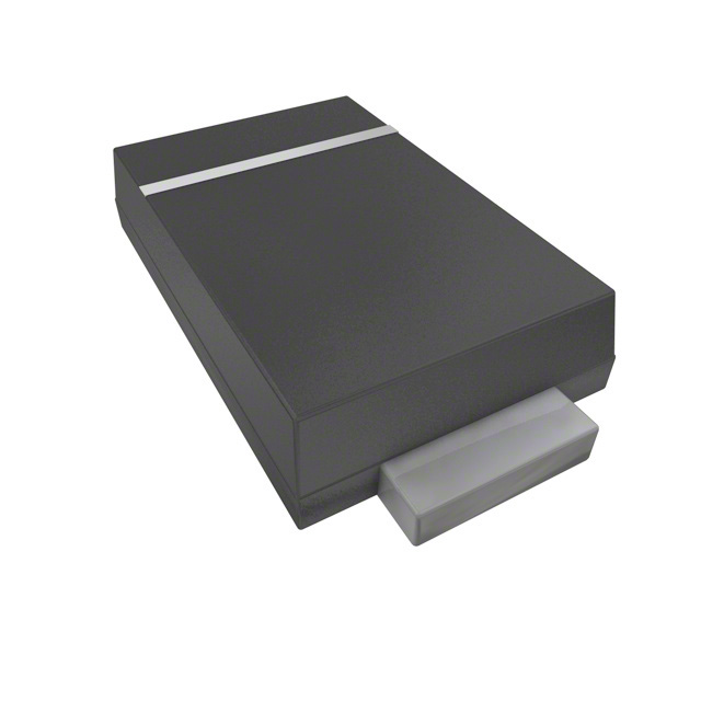


 工商网监
湘ICP备2023018690号
工商网监
湘ICP备2023018690号