Data Communications Family
Z380 Microprocessor
Product Specification
PS010002-0708
Copyright ©2008 by Zilog®, Inc. All rights reserved.
www.zilog.com
�Z380 Microprocessor
Product Specification
Warning: DO NOT USE IN LIFE SUPPORT
LIFE SUPPORT POLICY
ZILOG'S PRODUCTS ARE NOT AUTHORIZED FOR USE AS CRITICAL COMPONENTS IN LIFE
SUPPORT DEVICES OR SYSTEMS WITHOUT THE EXPRESS PRIOR WRITTEN APPROVAL OF
THE PRESIDENT AND GENERAL COUNSEL OF ZILOG CORPORATION.
As used herein
Life support devices or systems are devices which (a) are intended for surgical implant into the body, or (b)
support or sustain life and whose failure to perform when properly used in accordance with instructions for
use provided in the labeling can be reasonably expected to result in a significant injury to the user. A
critical component is any component in a life support device or system whose failure to perform can be
reasonably expected to cause the failure of the life support device or system or to affect its safety or
effectiveness.
Document Disclaimer
©2008 by Zilog, Inc. All rights reserved. Information in this publication concerning the devices,
applications, or technology described is intended to suggest possible uses and may be superseded. ZILOG,
INC. DOES NOT ASSUME LIABILITY FOR OR PROVIDE A REPRESENTATION OF ACCURACY
OF THE INFORMATION, DEVICES, OR TECHNOLOGY DESCRIBED IN THIS DOCUMENT.
Z I L O G A L S O D O E S N O T A S S U M E L I A B I L I T Y F O R I N T E L L E C T U A L P R O P E RT Y
INFRINGEMENT RELATED IN ANY MANNER TO USE OF INFORMATION, DEVICES, OR
TECHNOLOGY DESCRIBED HEREIN OR OTHERWISE. The information contained within this
document has been verified according to the general principles of electrical and mechanical engineering.
Z8, Z8 Encore!, Z8 Encore! XP, Z8 Encore! MC, Crimzon, eZ80, and ZNEO are trademarks or registered
trademarks of Zilog, Inc. All other product or service names are the property of their respective owners.
PS010002-0708
Page 2 of 125
�Z380 Microprocessor
Product Specification
Revision History
Each instance in Revision History reflects a change to this document from its previous
revision. For more details, refer to the corresponding pages and appropriate links in the
table below.
Date
Revision Level
Description
Page No
July 2008
02
Updated format to the latest PS
template
All
March 2001
01
Original Issue
All
PS010002-0708
Page 3 of 125
Revision History
�Z380 Microprocessor
Product Specification
FEATURES
PS010002-0708
•
•
•
Static CMOS Design with Low-Power Standby Mode Option
•
Enhanced Instruction Set that Maintains Object-Code Compatibility with Z80® and
Z180 Microprocessors
•
•
•
•
•
•
•
16-Bit (64K) or 32-Bit (4G) Linear Address Space
•
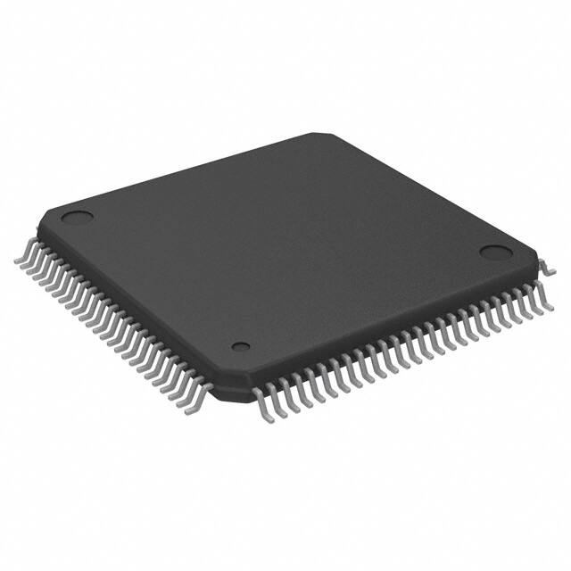
100-Pin QFP Package
32-Bit Internal Data Paths and ALU
Operating Frequency
– DC-to-18 MHz at 5V
– DC-to-10 MHz at 3.3V
16-Bit Data Bus with Dynamic Sizing
Two-Clock Cycle Instruction Execution Minimum
Four Banks of On-Chip Register Files
Enhanced Interrupt Capabilities, Including 16-Bit Vector
Undefined Opcode Trap for Z380™ Instruction Set
On-Chip I/O Functions:
– Six-Memory Chip Selects with Programmable Waits
– Programmable I/O Waits
– DRAM Refresh Controller
Page 4 of 125
�Z380 Microprocessor
Product Specification
GENERAL DESCRIPTION
The Z380 Microprocessor is an integrated high-performance microprocessor with fast and
efficient throughput and increased memory addressing capabilities. The Z380 offers a continuing growth path for present Z80-or Z180-based designs, while maintaining Z80® CPU
and Z180 MPU object-code compatibility. The Z380 MPU enhancements include an
improved 280 CPU, expanded 4-Gbyte space and flexible bus interface timing.
An enhanced version of the Z80 CPU is key to the Z380 MPU. The basic addressing
modes of the Z80 microprocessor have been augmented as follows: Stack Pointer Relative
loads and stores, 16-bit and 24-bit indexed offsets, and more flexible Indirect Register
addressing, with all of the addressing modes allowing access to the entire 32-bit address
space. Additions made to the instruction set, include a full complement of 16-bit arithmetic and logical operations, 16-bit I/O operations, multiply and divide, plus a complete set
of register-to-register loads and exchanges.
The expanded basic register file of the Z80 MPU microprocessor includes alternate register versions of the IX and IY registers. There are four sets of this basic Z80 microprocessor register file present in the Z380 MPU, along with the necessary resources to manage
switching between the different register sets. All of the register-pairs and index registers in
the basic Z80 microprocessor register file are expanded to 32 bits.
The Z380 MPU expands the basic 64 Kbyte Z80 and Z180 address space to a full 4 Gbyte
(32-bit) address space. This address space is linear and completely accessible to the user
program. The I/O address space is similarly expanded to a full 4 Gbyte (32-bit) range and
16-bit I/O, and both simple and block move are added.
Some features that have traditionally been handled by external peripheral devices have
been incorporated in the design of the Z380 microprocessor. The on-chip peripherals
reduce system chip count and reduce interconnection on the external bus. The Z380 MPU
contains a refresh controller for DRAMs that employs a /CAS-before-/RAS refresh cycle
at a programmable rate and burst size.
Six programmable memory-chip selects are available, along with programmable waitstate generators for each chip-select address range.
The Z380 MPU provides flexible bus interface timing, with separate control signals and
timing for memory and I/O. The memory bus control signals provide timing references
suitable for direct interface to DRAM, static RAM, EPROM, or ROM. Full control of the
memory bus timing is possible because the /WAIT signal is sampled three times during a
memory transaction, allowing complete user control of edge-to-edge timing between the
reference signals provided by the Z380 MPU. The I/O bus control signals allow direct
interface to members of the Z80 family of peripherals, the Z8000 family of peripherals, or
the Z8500 series of peripherals. Figure 1 shows the Z380 block diagram; Figure 2 shows
the pin assignments.
PS010002-0708
Page 5 of 125
�Z380 Microprocessor
Product Specification
All signals with a preceding front slash, "/", are active Low e.g., B//W (WORD is active
Low); B/W is active Low, only)
Note:
Clock with
Standby Control
External Interface Logic
/INT3-0
/NMI
/RESET
/BACK
/BREQ
I/O BUS CNTLS
MEM BUS CNTLS
VSS
/WAIT
GND
MSIZE
Ground
D15-0
VDD
A31-0
VCC
/LMCS/UMCS/MCS3-0
Power
/HALT
Device
/STNBY
Circuit
IOCLK
Connection
BUSCLK
CLKO
CLKI
CLKSEL
Power connections follow conventional descriptions below:
Interrupts
Chip Selects
and Waits
CPU
Refresh
Conrol
/EV
Data (16)
VDD
Address (32)
VSS
Figure 1. Z380 Functional Block Diagram
Figure 1. Z380 Functional Block Diagram
PS010002-0708
Page 6 of 125
�Z380 Microprocessor
Product Specification
A5
A4
A3
1
100
90
95
85
80
A24
2
A25
A26
A2
A1
A0
5
75
VSS
A31
VSS
10
70
D1
D2
Z380
100-Pin QFP
15
65
/MRD
/MWR
/MSIZE
/WAIT
BUSCLK
IOCLK
D3
D4
D5
D6
D7
20
60
/M1
/IORQ
/IORD
CLKI
CLKO
VDD
VSS
D0
/TREFA
/TREFC
/BHEN
/BLEN
A27
A28
A29
A30
VDD
VSS
VDD
/TREFR
A23
D8
D9
D10
D11
D12
25
55
/IOWR
D13
D14
VSS
D15
VDD
VSS
VDD
30
35
40
45
50
VSS
Figure 2. 100-Pin QFP Pin Assignments
PS010002-0708
Page 7 of 125
�Z380 Microprocessor
Product Specification
PIN DESCRIPTION
A31-A0 Address Bus (outputs, activeHigh, tri-state).These non-multiplexed address signals provide a linear memory address space of four gigabytes. The 32-address signals are
also used to access I/O devices.
/BACK Bus Acknowledge (output, active Low, tri-state). This signal, when asserted, indi-
cates that the Z380 MPU has accepted an external bus request and has tri-stated its output
drivers for the address bus, data bus and the bus control signals /TREFR, /TREFA, /
TREFC, /BHEN, /BLEN, /MRD, /MWR, /IORQ, /IORD, and /IOWR. Note that the Z380
MPU cannot provide any DRAM refresh transactions while it is in the bus acknowledge
state.
/BHEN Byte High Enable (output, active Low, tri-state). This signal is asserted at the
beginning of a memory, or refresh transaction to indicate that an operation on D15-D8 is
requested. For a 16-bit memory transaction, if /MSIZE is asserted, indicating a byte-wide
memory, another memory transaction is performed to transfer the data on D15-D8, this
time through D15-D8.
/BLEN Byte Low Enable (output, active Low, tri-state). This signal is asserted at the
beginning of a memory or refresh transaction to indicate that an operation on D7-D0 is
requested. For a 16-bit memory transaction, if /MSIZE is asserted, indicating a byte-wide
memory, only the data on D7-D0 will be transferred during this transaction, and another
transaction will be performed to transfer the data on D15-D8, this time through D7-D0.
/BREQ Bus Request (input, active Low). When this signal is asserted, an external bus
master is requesting control of the bus. /BREQ has higher priority than all nonmaskable
and maskable interrupt requests.
BUSCLK Bus Clock (output, active High, tri-state). This signal, output by the Z380 MPU,
is the reference edge for the majority of other signals generated by the Z380 MPU. BUSCLK is a delayed version of the CLK input.
CLKI Clock/Crystal (input, active High). An externally generated direct clock can be input
at this pin and the Z380 MPU would operate at the CLKI frequency. Alternatively, a crystal up to 20 MHz can be connected across CLKI and CLKO, and the Z380 MPU would
operate at half of the crystal frequency. The two clocking options are controlled by the
CLKsel input.
CLKO Crystal (output, active High). Crystal oscillator connection. This pin should be left
open if an externally generated direct clock is input at the CLKI pin.
CLKsel Clock Option Select (input, active High). This input should be connected to VDD
to select the direct clock option and should be connected to VSS for the crystal option.
D15-D0 Data Bus (input/outputs, active High, tri-state). This bi-directional 16-bit data
bus is used for data transfer between the Z380 MPU and memory or I/O devices. Note that
for a memory word transfer, the even-addressed (A0 = 0) byte is generally transferred on
D15-D8, and the odd-addressed (A0 = 1) byte on D7-D0 (see the /MSIZE pin description).
PS010002-0708
Page 8 of 125
�Z380 Microprocessor
Product Specification
/EV Evaluation Mode (input, active Low). This input should be left unconnected for nor-
mal operation. When it is driven to logic 0, the Z380 MPU conditions itself in the reset
mode and tri-states all of its output pin drivers.
/HALT Halt Status (output, active Low, tri-state). If the Z380 MPU standby mode option
is not selected, a Sleep instruction is executed no different than a Halt instruction, and the
one HALT signal goes active to indicate the CPU's HALT state. If the standby mode
option is selected, this signal goes active only at the Halt instruction execution.
/STNBY Standby Status (output, active Low, tri-state). If the Z380 MPU standby mode is
selected, executing a sleep instruction stops clocking within the Z380 MPU and at BUSCLK and IOCLK after which this signal is asserted. The Z380 MPU is then in the low
power standby mode, with all operations suspended.
/INT3-0 Interrupt Requests (inputs, active Low). These signals are four asynchronous
maskable interrupt inputs.
IOCLK I/O Clock (output, active High, tri-state). This signal is a program controlled
divided-down version of BUSCLK. The division factor can be two, four, six or eight with
I/O transactions and interrupt-acknowledge transactions occurring relative to IOCLK.
/INTAK Interrupt Acknowledge Status (output, active Low, tri-state). This signal is used to
distinguish between I/O and interrupt acknowledge transactions. This signal is High during I/O read and I/O write transactions and Low during interrupt acknowledge transactions.
/IORQ Input/Output Request (output, active Low, tri-state). This signal is active during all
I/O read and write transactions and interrupt acknowledge transactions.
/M1 Machine Cycle One (output, active Low, tri-state). This signal is active during inter-
rupt acknowledge and RETI transactions.
/IORD Input, Output Read Strobe (output, active Low, tri-state). This signal is used strobe
data from the peripherals during I/O read transactions. In addition, /IORD is active during
the special RETI transaction and the I/O heartbeat cycle in the Z80 protocol case.
/IOWR Input/Output Write Strobe (output, active Low, tri-state). This signal is used to
strobe data into the peripherals during I/O write transactions.
/LMCS Low Memory Chip Select (output, active Low, tri-state). This signal is activated
during a memory read or memory write transaction when accessing the lower portion of
the linear address space within the first 16 Mbytes, but only if this chip select function is
enabled.
/MCS3-/MCS0 Mid-range Memory Chip Selects (output, active Low, tri-state). These sig-
nals are individually active during memory read or write transactions when accessing the
mid-range portions of the linear address space within the first 16 Mbytes. These signals
can be individually enabled or disabled.
/MRD Memory Read (output, active Low, tri-state). This signal indicates that the
addressed memory location should place its data on the data bus as specified by the /
PS010002-0708
Page 9 of 125
�Z380 Microprocessor
Product Specification
BHEN and /BLEN control signals. /MRD is active from the end of T1 until the end of T4
during memory read transactions.
/MSIZE Memory Size (input, active Low). This input, from the addressed memory location, indicates if it is word size (logic High) or byte size (logic Low). In the latter case, the
addressed memory should be connected to the D15-D8 portion of the data bus, and an
additional memory transaction will automatically be generated to complete a word size
data transfer.
/MWR Memory Write (output, active Low, tri-state). This signal indicates that the
addressed memory location should store the data on the data bus, as specified by the /
BHEN and /BLEN control signals. /MWR is active from the end of T2 until the end of T4
during memory write transactions.
/NMI Nonmaskable Interrupt(input, falling edge-triggered). This input has higher priority
than the maskable interrupt inputs /INT3-INT0.
/RESET Reset (input, active Low). This input must be active for a minimum of five BUSCLK periods to initialize the Z380 MPU. The effect of /RESET is described in detail in
the Reset section.
/TREFA Timing Reference A (output, active Low, tri-state). This timing reference signal
goes Low at the end of T2 and returns High at the end of T4 during a memory read, memory write or refresh transaction. It can be used to control the address multiplexer for a
DRAM interface or as the /RAS signal at higher processor clock rates.
/TREFC Timing Reference C (output, activeLow, tri-state). This timing reference signal
goes Low at the end of T3 and returns High at the end of T4 during a memory read, memory write or refresh transaction. It can be used as the /CAS signal for DRAM accesses.
/TREFR Timing Reference R (output, active Low, tri-state). This timing reference signal
goes Low at the end of T1 and returns High at the end of T4 during a memory read, memory write or refresh transaction. It can be used as the /RAS signal for DRAM accesses.
/UMCS Upper Memory ChipSelect (output, active Low, tri-state). This signal is activated
during a memory read, memory write, or optionally a refresh transaction when accessing
the highest portion of the linear address space within the first 16 Mbytes, but only if this
chip select function is enabled.
VDD Power Supply. These eight pins carry power to the device. They must be tied to the
same voltage externally.
VSS Ground. These eight pins are the ground references for the device. They must be tied
to the same voltage externally.
/WAIT Wait (input, active Low). This input is sampled by BUSCLK or IOCLK, as appropriate, to insert Wait states into the current bus transaction.
The conditioning and characteristics of the Z380 MPU pins under various operation
modes are defined in Table 1.
PS010002-0708
Page 10 of 125
�Z380 Microprocessor
Product Specification
Table 1. Z380 MPU Pin ConditioningpCharacteristics Operation Mode Conditions
Pin
Names
Normal
/BREQ=1,/BACK=1,
/EV=NC
Bus Relinquish
/BREQ=0,/BACK=0,
/EV=NC
Evaluation
CLKI
CLKO
CLKSEL
BUSCLK
IOCLK
A31-A0
Input
Output/No Connection
Input
Output
Output
Output
Input
Output/No Connection
Input
Output
Output
Tri-state
Input
No Connection
Input
Tri-state
Tri-state
Tri-state
D15-D0
/TREFR,/TREFA,
/TREFC
/MRD,/MWR
/BHEN,/BLEN
/LMCS,/UMCS,
/MCS3-MCS0
Input/Output
Output
Tri-state
Tri-state
Tri-state
Tri-state
Output
Output
Output
Tri-state
Tri-state
Tri-state
Tri-state
Tri-state
Tri-state
/MSIZE,/WAIT
/HALT,/STNBY
/M1,/INTAK
/IORQ,/IORD,
/IOWR
/BREQ
/BACK
Input
Output
Output
Output
Input
Output
Output
Tri-state
Input
Tri-state
Tri-state
Tri-state
Input
Output
Input
Output
Input
Tri-state
/NMI,/INT3-/INT0
/RESET
/EV
VDD
VSS
Input
Input
No Connection
Power
Ground
Input
Input
No Connection
Power
Ground
Input
Input
Input
Power
Ground
EXTERNAL INTERFACE
Two kinds of operations can occur on the system bus: transactions and requests. At any
given time, one device (either the CPU or a bus master) has control of the bus and is
known as the bus master.
This section shows all of the transaction and request timing for the device. For the sake of
clarity, there are more figures than are actually necessary. This should aid the reader rather
than confuse. In all of the timing diagram figures, the row labelled STATUS encompasses
/BHEN, /BLEN, and the chip select signals.
PS010002-0708
Page 11 of 125
�Z380 Microprocessor
Product Specification
Transactions
A transaction is initiated by the bus master and is responded to by some other device on
the bus. Only one transaction can proceed at a time; six kinds of transactions can occur:
Memory, Refresh, I/O, Interrupt Acknowledge, RETI (Return from Interrupt), and Halt.
The Z380 MPU is unique in that memory and I/O bus transactions use separate control
signals. This allows the memory interface to be optimized independently of the I/O interface.
Memory Transactions
Memory transactions move instructions or data to or from memory when the Z380 MPU
performs a memory access. Thus, they are generated during program execution to fetch
instructions from memory and to fetch and store memory data. They are also generated to
store old program status and fetch new program status during interrupt and trap handling,
and are used by DMA peripherals to transfer information. A memory transaction is two
clock cycles long unless extended with wait states. Wait states may be inserted between
each of the four T states in a memory transaction and are one BUSCLK cycle long per
wait state. The external /WAIT input is sampled only after any internally-generated wait
states are inserted. Memory transactions may transfer either bytes or words. If the Z380
MPU attempts to transfer a word to a byte-wide memory, the /MSIZE signal should be
asserted Low to force this transaction to be byte-wide dynamically. The Z380 MPU will
then perform another memory transaction to transfer the byte that was not transferred during the first transaction.
Read memory transactions are shown without wait states, with wait states between T1 and
T2, between T2 and T3, and between T3 and T4 (Figures 3 - 6). The data bus is driven by
the memory being addressed, and the memory data is latched immediately before the rising edge of BUSCLK which terminates T4.
PS010002-0708
Page 12 of 125
�Z380 Microprocessor
Product Specification
T1
T2
T3
T4
BUSCLK
ADDRESS
DATA
STATUS
/WAIT
/MSIZE
/TREFR
/TREFA
/TREFC
/MRD
/MWR
Figure 3. Read Cycle, No Waits
PS010002-0708
Page 13 of 125
�Z380 Microprocessor
Product Specification
T1
T1L
T1H
T2
T3
T4
BUSCLK
ADDRESS
DATA
STATUS
/WAIT
/MSIZE
/TREFR
/TREFA
/TREFC
/MRD
/MWR
Figure 4. Read Cycle, T1 Wait
PS010002-0708
Page 14 of 125
�Z380 Microprocessor
Product Specification
(Continued)
T1
T2
T2H
T2L
T3
T4
BUSCLK
ADDRESS
DATA
STATUS
/WAIT
/MSIZE
/TREFR
/TREFA
/TREFC
/MRD
/MWR
Figure 5. Read Cycle, T2 Wait
PS010002-0708
Page 15 of 125
�Z380 Microprocessor
Product Specification
T1
T2
T3
T3L
T3H
T4
BUSCLK
ADDRESS
DATA
STATUS
/WAIT
/MSIZE
/TREFR
/TREFA
/TREFC
/MRD
/MWR
Figure 6. Read Cycle, T3 Wait
PS010002-0708
Page 16 of 125
�Z380 Microprocessor
Product Specification
EXTERNAL INTERFACE (Continued)
Write memory transactions are shown without wait states, with wait states between T1 and
T2, between T2 and T3, and between T3 and T4 (Figures 7-10). The /MWR strobe is activated at the end of T1, to allow write data setup time for the memory since the write data is
driven on to the data bus at the beginning of T1.
T1
T2
T3
T4
BUSCLK
ADDRESS
DATA
STATUS
/WAIT
/MSIZE
/TREFR
/TREFA
/TREFC
/MRD
/MWR
Figure 7. Write Cycle, No Waits
PS010002-0708
Page 17 of 125
�Z380 Microprocessor
Product Specification
T1
T1L
T1H
T2
T3
T4
BUSCLK
ADDRESS
DATA
STATUS
/WAIT
/MSIZE
/TREFR
/TREFA
/TREFC
/MRD
/MWR
Figure 8. Write Cycle, T1 Wait
PS010002-0708
Page 18 of 125
�Z380 Microprocessor
Product Specification
T1
T2
T2H
T2L
T3
T4
BUSCLK
ADDRESS
DATA
STATUS
/WAIT
/MSIZE
/TREFR
/TREFA
/TREFC
/MRD
/MWR
Figure 9. Write Cycle, T2 Wait
PS010002-0708
Page 19 of 125
�Z380 Microprocessor
Product Specification
T1
T2
T3
T3L
T3H
T4
BUSCLK
ADDRESS
DATA
STATUS
/WAIT
/MSIZE
/TREFR
/TREFA
/TREFC
/MRD
/MWR
Figure 10. Write Cycle, T3 Wait
PS010002-0708
Page 20 of 125
�Z380 Microprocessor
Product Specification
EXTERNAL INTERFACE (Continued)
Refresh Transactions
A memory refresh transaction is generated by the Z380 MPU refresh controller and can
occur immediately after the final clock cycle of any other transaction. The address during
the refresh transaction is not defined as the CAS-before-RASrefresh cycle is assumed,
which uses the on-chip refresh address generator present on DRAMs. Prior to the first
refresh transaction, a refresh setup cycle is performed to guarantee that the /CAS precharge time is met. This refresh setup cycle is present only prior to the first refresh transaction in a burst (Figure 11). Refresh transactions are shown without wait states, with wait
states between T1 and T2, between T2 and T3, and between T3 and T4 (Figures 12-15).
Note that during the refresh cycle the data bus is continuously driven, /MRD and /MWR
remain inactive, /BHEN and /BLEN are active to enable all /CAS signals to the DRAMS,
and those Chip Select signals enabled for DRAM refresh transactions are active.
TPH
TPL
BUSCLK
ADDRESS
DATA
STATUS
/WAIT
/MSIZE
/TREFR
/TREFA
/TREFC
/MRD
/MWR
Figure 11. Refresh Setup
PS010002-0708
Page 21 of 125
�Z380 Microprocessor
Product Specification
T1
T2
T3
T4
BUSCLK
ADDRESS
DATA
STATUS
/WAIT
/MSIZE
/TREFR
/TREFA
/TREFC
/MRD
/MWR
Figure 12. Refresh Cycle, No Waits
PS010002-0708
Page 22 of 125
�Z380 Microprocessor
Product Specification
T1
T1L
T1H
T2
T3
T4
BUSCLK
ADDRESS
DATA
STATUS
/WAIT
/MSIZE
/TREFR
/TREFA
/TREFC
/MRD
/MWR
Figure 13. Refresh Cycle, T1 Wait
PS010002-0708
Page 23 of 125
�Z380 Microprocessor
Product Specification
T1
T2
T2H
T2L
T3
T4
BUSCLK
ADDRESS
DATA
STATUS
/WAIT
/MSIZE
/TREFR
/TREFA
/TREFC
/MRD
/MWR
Figure 14. Refresh Cycle, T2 Wait
PS010002-0708
Page 24 of 125
�Z380 Microprocessor
Product Specification
T1
T2
T3
T3L
T3H
T4
BUSCLK
ADDRESS
DATA
STATUS
/WAIT
/MSIZE
/TREFR
/TREFA
/TREFC
/MRD
/MWR
Figure 15. Refresh Cycle, T3 Wait
PS010002-0708
Page 25 of 125
�Z380 Microprocessor
Product Specification
I/O Transactions
I/O transactions move data to or from an external peripheral when the Z380 MPU performs an I/O access. All I/O transactions occur referenced to the IOCLK signal, when it is
a divided-down version of the BUSCLKsignal. BUSCLK may be divided by a factor of
from two to eight to form the IOCLK, under program control. An example of this division
is shown, for the four possible divisors, in Figure 16. Note that the IOCLK divider is synchronized (i.e., starts with a known timing relationship) at the trailing edge of /RESET.
This is discussed in the Reset Section.
BUSCLK
IOCLK (X2)
IOCLK (X4)
IOCLK (X6)
IOCLK (X8)
Figure 16. IOCLK Timing
EXTERNAL INTERFACE (Continued)
The Z380 MPU is unique in that it employs separate control signals for accessing the
memory and I/O. This allows the two interfaces to be optimized independent of one
another. The I/O bus control signals allow direct connection to members of the Z80 family
of peripherals or the Z8500 family of peripherals.
Note that because all I/O bus transactions start on a rising edge of IOCLK, there may be
up to n BUSCLK cycles of latency between the execution unit request for the transaction
and the transaction actually starting, where n is the programmed clock divisor for IOCLK.
This implies that the lowest possible divisor should always be used for IOCLK.
All I/O transactions are four IOCLK cycles long unless extended by Wait states. Wait
states may be inserted between the third and fourth IOCLK cycles in an I/O transaction
and are one IOCLK cycle per wait state. The external /WAIT input is sampled only after
internally-generated wait states are inserted.
PS010002-0708
Page 26 of 125
�Z380 Microprocessor
Product Specification
I/O Read transactions are shown with and without a wait state (Figures 17-18). The contents of the data bus is latched immediately before the falling edge of IOCLK during the
last IOCLK cycle of the transaction.
IOCLK
ADDRESS
DATA
/WAIT
/MI
/IORQ
/IORD
/IOWR
/INTAK
Fi
8A I/O R d C l N W it
Figure 17. I/0Read Cycle, No Waits
PS010002-0708
Page 27 of 125
�Z380 Microprocessor
Product Specification
IOCLK
ADDRESS
DATA
/WAIT
/MI
/IORQ
/IORD
/IOWR
/INTAK
Fi
8B I/O R
dC
l
T1 W it
Figure 18. I/O Read Cycle, T1 Wait
PS010002-0708
Page 28 of 125
�Z380 Microprocessor
Product Specification
EXTERNAL INTERFACE (Continued)
I/O Write transactions are shown with and without a wait state (Figures 19-20). The data
bus is driven throughout the transaction.
IOCLK
ADDRESS
DATA
/WAIT
/MI
/IORQ
/IORD
/IOWR
/INTAK
Figure 19. I/O Write Cycle, No Waits
PS010002-0708
Page 29 of 125
�Z380 Microprocessor
Product Specification
ZILOG
MICROPROCE
IOCLK
ADDRESS
DATA
/WAIT
/MI
/IORQ
/IORD
/IOWR
/INTAK
Figure 20. I/O Write Cycle, T1 Wait
PS010002-0708
Page 30 of 125
�Z380 Microprocessor
Product Specification
EXTERNAL INTERFACE (Continued)
Interrupt Acknowledge Transactions
An interrupt acknowledge transaction is generated by the Z380 MPU in response to an
unmasked external interrupt request. Figure 21 shows an interrupt acknowledge transaction in response to /INT0 and Figure 22 shows an interrupt acknowledge transaction in
response to either one of /INT-3. Note that because all I/O bus transactions start on a rising
edge of IOCLK, there may be up to n BUSCLK cycles of latency between the execution
unit request for the transaction and the transaction actually starting (where n is the programmed clock divisor for IOCLK).
IOCLK
ADDRESS
DATA
/WAIT
/M1
/IORQ
/IORD
/IOWR
/INTAK
Figure 21. Interrupt Acknowledge Cycle, /INT0
PS010002-0708
Page 31 of 125
�Z380 Microprocessor
Product Specification
IOCLK
ADDRESS
DATA
/WAIT
/MI
/IORQ
/IORD
/IOWR
/INTAK
Figure 22. Interrupt Acknowledge Cycle, /INT3-1
An interrupt acknowledge transaction for /INT0 is five IOCLK cycles long unless
extended by Wait states. /WAIT is sampled at two separate points during the transaction.
/WAIT is first sampled at the end of the first IOCLK cycle during the transaction. Wait
states inserted here allow the external daisy-chain between peripherals with a longer time
to settle before the interrupt vector is requested. /WAIT is then sampled at the end of the
fourth IOCLK cycle to delay the point at which the interrupt vector is read by the Z380
MPU, after it has been requested.
The interrupt vector may be either eight or sixteen bits, under program control, and is
latched by the falling edge of IOCLK in the last cycle of the interrupt acknowledge transaction. When using Mode 0 interrupts, where the Z380 MPU fetches an instruction from
the interrupting device, these fetches are always eight bits wide and are transferred over
D7-D0.
PS010002-0708
Page 32 of 125
�Z380 Microprocessor
Product Specification
An interrupt acknowledge transaction in response to one of /INT3-/INT1 is also five
IOCLK cycles long, unless extended by wait states. The waits are sampled and inserted at
similar locations as an interrupt acknowledge transaction is for /INT0. Note, however,
only the /INTAK signal is active with /MI, /IORQ, /IORD and /IOWR held inactive.
For either type of INTACK transaction the address bus is driven with a value which indicates the type of interrupt being acknowledged as follows: A31-A6 are all one, and A3-A0
are one except for a single zero corresponding to the maskable interrupt being acknowledged. Thus an /INT3 acknowledge is signaled by A3 being zero during the interrupt
acknowledge transaction, /INT2 acknowledge is signalled by A2 being zero, etc.
RETI Transactions
The RETI transaction is generated whenever an RETI instruction is executed by the Z380
MPU. This transaction is necessary because Z80 family peripherals are designed to watch
instruction fetches and take special action upon seeing a RETI instruction (this is the only
instruction that the Z80 family peripherals watch for). Since the Z380 MPU fetches
instructions using the memory control signals, a simulated RETI instruction fetch must be
placed on the bus with the appropriate I/O bus control signals. This is shown in Figure 23.
Again, note that because all I/O bus transactions start on a rising edge of IOCLK, there
may be up to n BUSCLK cycles of latency between the execution unit request for the
transaction and the transaction actually starting, where n is the programmed clock divisor
for IOCLK.
PS010002-0708
Page 33 of 125
�Z380 Microprocessor
Product Specification
1
2
3
4
5
6
7
8
9
10
IOCLK
ADDRESS
DATA
EDED
4D4D
/WAIT
/M1
/IORQ
/IORD
/IOWR
/INTAK
Figure 23. Return From Interrupt Cycle
The RETI transaction is ten IOCLK cycles long unless extended by Wait states, and
/WAIT is sampled at three separate points during the transaction. /WAIT is first sampled in
the middle of the third IOCLK cycle to allow for longer/IORDLow-time requirements.
/WAIT is then sampled again during the middle of the fifth IOCLK cycle to allow for longer internal daisy-chain settling time within the peripheral. Wait states inserted here have
the effect of separating what the peripheral sees as two separate instruction fetch cycles.
Finally, /WAIT is sampled in the middle of the ninth IOCLK cycle, again to allow for longer /IORD Low-time requirements.
The Z380 MPU drives the data bus throughout the RETI transaction, with EDEDH during
the first half of the transaction (the first byte of a RETI instruction is EDH) and with
4D4DH during the second half of the transaction (the second byte of an RETI instruction
is 4DH).
PS010002-0708
Page 34 of 125
�Z380 Microprocessor
Product Specification
HALT Transactions
A HALT transaction occurs whenever the Z380 MPU executes a Halt instruction, with the
/HALT signal activated on the falling edge of BUSCLK. If the standby mode is not
enabled, executing a Sleep instruction would also cause a Halt transaction to occur. While
in the Halt state, the Z380 MPU continues to drive the address and data buses, and the
/HALT signal remains active until either an interrupt request is acknowledged or a reset is
received. Refresh transactions may occur while in the halt state and the bus can be granted.
The timing of entry into the Halt state is shown in Figure 24, while the timing of exiting
from Halt state is shown in Figure 25.
T5
THL
THH
THL
BUSCLK
ADDRESS
DATA
STATUS
/WAIT
/MSIZE
/TREFR
/TREFA
/TREFC
/MRD
/MWR
/HALT
Figure 24. HALT Entry
PS010002-0708
Page 35 of 125
�Z380 Microprocessor
Product Specification
THH
THL
THH
THL
THH
T6
BUSCLK
ADDRESS
DATA
STATUS
/WAIT
/MSIZE
/TREFR
/TREFA
/TREFC
/MRD
/MWR
/HALT
/INT or /NMI
Figure 25. HALT Exit
PS010002-0708
Page 36 of 125
�Z380 Microprocessor
Product Specification
Requests
A request can be initiated by a device that does not have control of the bus. Two types of
request can occur: Bus request and Interrupt request. When an interrupt or bus request is
made, it is answered by the CPU according to its type. For an interrupt request, the CPU
initiates an interrupt acknowledge transaction and for bus requests, the CPU enters the bus
disconnect state, relinquishes the bus, and activates an Acknowledge signal.
BUS Requests
To generate transactions on the bus, a potential bus master (such as a DMA controller)
must gain control of the bus by making a bus request. A bus request is initiated by driving
/BREQ Low. Several bus requesters may be wired-OR to the /BREQ pin; priorities are
resolved externally to the CPU, usually by a priority daisy chain.
The asynchronous /BREQ signal generates an internal /BUSREQ, which is synchronous.
If the /BREQ is active at the beginning of any transaction, the internal /BUSREQ causes
the /BACK signal to be asserted after the current transaction is completed. The Z380 MPU
then enters the Bus Disconnect state and gives up control of the bus. All Z380 MPU control signals, except /BACK, /MI and /INTAK are tri-stated. Note that release of the bus
may be inhibited under program control to allow the Z380 MPU exclusive access to a
shared resource; this is controlled by the SETC LCK and RESC LCK instructions. Entry
into the Bus Disconnect state is shown in Figure 26. The Z380 MPU regains control of the
bus after /BREQ is deasserted. This is shown in Figure 27.
Interrupt Requests
The Z380 MPU supports two types of interrupt requests, maskable /INT3-INT0 and nonmaskable (/NMI). The interrupt request line of a device that is capable of generating an
interrupt can be tied to either /NMI or one of the maskable interrupt request lines, and several devices can be connected to one interrupt request line with the devices arranged in a
priority daisy chain. However, because of the need for Z80 family peripheral devices to
see the RETI instruction, only one daisy chain of Z80-family peripherals can be used. The
Z380 MPU handles maskable and nonmaskable interrupt requests somewhat differently,
as follows:
Any High-to-Low transition on the /NMI input is asynchronously edge-detected, and the
internal NMI latch is set. At the beginning of the last clock cycle in the last internal
machine cycle of any instruction, the maskable interrupts are sampled along with the state
of the NMI latch.
If an enabled maskable interrupt is requested, at the next possible time (the next rising
edge of IOCLK) an interrupt acknowledge transaction is generated to fetch the interruptvector from the interrupting device.For a nonmaskable interrupt, no interrupt acknowledge
transaction is generated; the NMI service routine always starts at address 00000066H.
PS010002-0708
Page 37 of 125
�Z380 Microprocessor
Product Specification
Transaction in progress
T7
TBL
BUSCLK
ADDRESS
DATA
STATUS
/WAIT
/MSIZE
/TREFR
/TREFA
/TREFC
/MRD
/MWR
/BREQ
/BACK
/MI
/IORQ
/IORD
/IOWR
/INTAK
Figure 26. Bus Request/Acknowledge Cycle
PS010002-0708
Page 38 of 125
�Z380 Microprocessor
Product Specification
TBH
TBL
TBH
TBL
TBH
TIL
BUSCLK
ADDRESS
DATA
STATUS
/WAIT
/MSIZE
/TREFR
/TREFA
/TREFC
/MRD
/MWR
/BREQ
/BACK
/MI
/IORQ
/IORD
/IOWR
/INTAK
Figure 27. Bus Request/Acknowledge End Cycle
PS010002-0708
Page 39 of 125
�Z380 Microprocessor
Product Specification
EXTERNAL INTERFACE (Continued)
Miscellaneous Timing
There are two cases where a specific transaction is not taking place on the bus which are
illustrated in this section: the bus idle cycle and the I/O heartbeat cycle.
Idle Cycles
When no transactions are being performed on the bus, an idle cycle occurs (Figure 16). All
control signals, for both memory and I/O, are inactive during the Idle cycle.
TiH
TiL
BUSCLK
ADDRESS
DATA
STATUS
/WAIT
/MSIZE
/TREFR
/TREFA
/TREFC
/MRD
/MWR
Figure 28. Idle Cycle
PS010002-0708
Page 40 of 125
�Z380 Microprocessor
Product Specification
I/O Heartbeat Cycle
The Z380 MPU is capable of generating an I/O heartbeat cycle on the I/O bus in response
to an I/O write to an on-chip control register. This cycle is most useful with Z80 family
peripherals, where some members require a transaction that looks like a Z80 CPU instruction fetch to perform certain interrupt functions (Figure 29).
IOCLK
ADDRESS
DATA
All Zeros
/WAIT
/MI
/IORQ
/IORD
/IOWR
/ INTAK
Figure 29. I/O Heartbeat Cycle
PS010002-0708
Page 41 of 125
�Z380 Microprocessor
Product Specification
EXTERNAL INTERFACE (Continued)
Reset Timing
The timing for entering and exiting the reset state is shown in Figures 30 and 31. The
effects of reset on the internal state of the Z380 MPU are detailed in the Reset section.
The synchronization of IOCLK at the end of the reset state is shown in Figure 32. Note
that the IOCLK divisor is set to the maximum value (eight) by /RESET and is only synchronized at the end of the reset state.
Transaction in progress
T9
TRL
BUSCLK
ADDRESS
DATA
STATUS
/WAIT
/MSIZE
/TREFR
/TREFA
/TREFC
/MRD
/MWR
/IOCTL3-0
/RESET
Figure 30. Reset Entry
PS010002-0708
Page 42 of 125
�Z380 Microprocessor
Product Specification
TRH
TRL
TRH
TRL
TRH
TiL
BUSCLK
ADDRESS
DATA
STATUS
/WAIT
/MSIZE
/TREFR
/TREFA
/TREFC
/MRD
/MWR
/IOCTL3-0
/RESET
Figure 31. Reset Exit
PS010002-0708
Page 43 of 125
�Z380 Microprocessor
Product Specification
EXTERNAL INTERFACE (Continued
BUSCLK
/RESET
IOCLK
Figure 32. IOCLK Reset Start-up
PS010002-0708
Page 44 of 125
�Z380 Microprocessor
Product Specification
CPU ARCHITECTURE
The Central Processing Unit (CPU) of the Z380 MPU is a binary-compatible extension of
the Z80 CPU and Z180 CPU architectures. High throughput rates for the Z380 CPU are
achieved by a high clock rate, high bus bandwidth and instruction fetch/execute overlap.
Communicating to the external world through an 8-or 16-bit data bus, the Z380 CPU is a
full 32-bit machine internally, with a 32-bit ALU and 32-bit registers.
Modes Of Operation
The Z380 CPU can operate in either Native or Extended mode, as controlled by a bit in the
Select Register (SR). In Native mode (the Reset configuration), all address manipulations
are performed modulo 65536 (16 bits). In this mode the Program Counter (PC) only increments across 16 bits, all address manipulation instructions (increment, decrement, add,
subtract, indexed, stack relative, and PC relative) only operate on 16 bits, and the Stack
Pointer (SP) only increments and decrements across 16 bits. The program counter highorder word is left at all zeros, as is the high-order words of the stack pointer and the I register. Thus Native mode is fully compatible with the Z80 CPU's 64 Kbyte address space. It
is still possible to address memory outside of the 64 Kbyte address space for data storage
and retrieved in Native mode, however, direct addresses, indirect addresses, and the highorder word of the SP, I and the IX and IY registers may be loaded with non-zero values.
But executed code and interrupt service routines must reside in the lowest 64 Kbytes of the
address space.
In Extended mode, however, all address manipulation instructions operate on 32 bits,
allowing access to the entire 4 Gbyte address space of the Z380 MPU. In both Native and
Extended modes, the Z380 CPU drives all 32 bits of the address onto the external address
bus; only the width of manipulated addresses distinguish Native from Extended mode.
The Z380 CPU implements one instruction to allow switching from Native to Extended
mode, but once in Extended mode, only Reset returns the Z380 MPU to Native mode. This
restriction applies because of the possibility of "misplacing" interrupt service routines or
vector tables during the translation from Extended mode back to Native mode.
In addition to Native and Extended mode, which is specific to memory space addressing,
the Z380 MPU can operate in either Word or Long Word mode specific to data load and
exchange operations. In Word mode (the reset configuration), all word load and exchange
operations manipulate 16-bit quantities. For example, only the low-order words of the
source and destination are exchanged in an exchange operation, with the high-order words
unaffected. In Long Word mode, all 32 bits of the source and destination are directives to
allow switching between Word and Long Word mode; SETC LW (Set Control Long
Word) and RESC LW (Reset Control Long Word) perform a global switch, while DDIR
W, DDIR LW and their variants are decoder directives that select a particular mode only
for the instruction that they precede.
Note that all word data arithmetic (as opposed to address manipulation arithmetic), rotate,
shift and logical operations are always in 16-bit quantities. They are not controlled by
either the Native/Extended or Word/Long Word selections. The exceptions to the 16-bit
PS010002-0708
Page 45 of 125
�Z380 Microprocessor
Product Specification
quantities are, of course, those multiply and divide operations with 32-bit products or dividends.
Lastly, all word Input/Output operations are performed on 16-bit values.
Address Spaces
The Z380 CPU architecture supports five distinct address spaces corresponding to the different types of locations that can be accessed by the CPU. These five address spaces are:
CPU register space, CPU control register space, memory address space, and I/O address
space (on-chip and external).
CPU Register Space
The CPU register space is shown in Figure 33 and consists of all of the registers in the
CPU register file. These CPU registers are used for data and address manipulation, and are
an extension of the Z80 CPU register set, with four sets of this extended Z80 CPU register
set present in the Z380 CPU. Access to these registers is specified in the instruction, with
the active register set selected by bits in the Select Register (SR) in the CPU control register space.
4 Sets of Registers
BCz
DEz
A
F
B
D
C
E
HLz
H
L
IXz
IXU
IXL
IYz
IYU
IYL
A'
F'
BCz'
B'
C'
DEz'
D'
E'
HLz'
H'
L'
IXz'
IXU'
IXL'
IYz'
IYU'
IYL'
R
Iz
I
SPz
SP
PCz
PC
Figure 33. Register Set
PS010002-0708
Page 46 of 125
�Z380 Microprocessor
Product Specification
Each register set includes the primary registers A, F, B, C, D, E, H, L, IX, and IY, as well
as the alternate registers A’, F’, B’, C’, D’, E’, H’, L’, IX’, and IY’. These byte registers
can be paired B with C, D with E, H with L, B’ with C’, D’ with E’ and H’ with L’ to form
word registers. These word registers are extended to 32 bits with the z extension to the
register. This register extension is only accessible when using the register as a 32-bit register (the Long Word mode) or when swapping between the most-significant and least-significant word of a 32-bit register. Whenever an instruction refers to a word register, the
implicit size is controlled by the Word or Long Word mode. Also included are the R, I and
SP registers, as well as the PC.
CPU Control Register Space
The CPU control register space consists of the 32-bit Select Register (SR), Figure 34. The
SR may be accessed as a whole or the upper three bytes of the SR may be accessed individually as the YSR, XSR, and DSR. In addition, these upper three bytes can be loaded
with the same byte value. The SR may also be PUSHed and POPed and is cleared to all
zeros on Reset.
YSR
XSR
Reserved (0)
31
30
29
28
27
IYBANK
IYP
Reserved (0)
26
25
24
23
22
21
MAINBANK
ALT
XM
LW
IEF1
8
7
6
5
IXBANK
20
19
18
17
0
LCK
2
1
IXP
16
DSR
Reserved (0)
15
14
13
12
11
10
9
IM
4
3
AFP
0
Figure 34. Select Register
IYBANK (IY Bank Select). This 2-bit field selects the register set to be used for the IY and
IY' registers. This field can be set independently of the register set selection for the other
Z380 CPU registers. Reset selects Bank 0 for IY and IY'.
IYP (IYPrime Register Select). This bit controls and reports whether IY or IY' is the cur-
rently active register. IY is selected when this bit is cleared and IY' is selected when this
bit is set. Reset clears this bit and selects IY.
IXBANK (IX Bank Select). This 2-bit field selects the register set to be used for the IX and
IX' registers. This field can be set independently of the register set selection for the other
Z380 CPU registers. Reset selects Bank 0 for IX and IX'.
PS010002-0708
Page 47 of 125
�Z380 Microprocessor
Product Specification
IXP (IXPrime Register Select). This bit controls and reports whether IX or IX' is the cur-
rently active register. IX is selected when this bit is cleared and IX' is selected when this
bit is set. Reset clears this bit and selects IX.
MAINBANK (Main Bank Select). This 2-bit field selects the register set to be used for the
A, F, BC, DE, HL, A', F', BC', DE' and HL' registers. This field can be set independently
of the register set selection for the other Z380 CPU registers. Reset selects Bank 0 for
these registers.
ALT (BC/DE/HL or BC'/DE'/HL' Register Select). This bit controls and reports whether
BC/DE/HL or BC'/DE'/HL' is the currently active bank of registers. BC/DE/HL are
selected when this bit is cleared and BC'/DE'/HL' are selected when this bit is set. Reset
clears this bit, selecting BC/DE/HL.
XM (Extended Mode). This bit controls the Extended/ Native mode selection for the Z380
CPU. This bit is set by the SETC XM instruction, and once set, it can be cleared only by a
reset on the /RESET pin. When this bit is set, the Z380 CPU is in Extended mode. Reset
clears this bit and the Z380 CPU is in Native mode.
LW (Long Word Mode). This bit controls the Long Word/ Word mode selection for the
Z380 CPU. This bit is set by the SETC LW instruction and cleared by the RESC LW
instruction. When this bit is set, the Z380 CPU is in Long Word mode; when this bit is
cleared, the Z380 CPU is in Word mode. Reset clears this bit. Note that individual instructions may be executed in either Word or Long Word load and exchange mode, using the
DDIR W and DDIR LW decoder directives.
IEF1 (Interrupt Enable Flag). This bit is the master Interrupt Enable for the Z380 CPU.
This bit is set by the EI instruction and cleared by the DI instruction. When this bit is set,
interrupts are enabled; when this bit is cleared, interrupts are disabled. Reset clears this bit.
IM (Interrupt Mode). This 2-bit field controls the interrupt mode for the /INT0 interrupt
request. These bits are controlled by the IM instructions (00 = IM 0, 01 = IM 1, 10 = IM 2,
11 = IM 3). Reset clears both of these bits, selecting Interrupt Mode 0.
LCK (Lock). This bit controls the Lock/Unlock status of the Z380 CPU. This bit is set by
the SETC LCK instruction and cleared by the RESC LCK instruction. When this bit is set,
no bus requests are accepted, providing exclusive access to the bus by the Z380 CPU.
When this bit is cleared the Z380 CPU will grant bus requests in the normal fashion. Reset
clears this bit.
AFP (AF Prime Register Select). This bit controls and reports whether AF or AF' is the
currently active pair of registers. AF is selected when this bit is cleared and AF' is selected
when this bit is set. Reset clears this bit and selects AF.
Memory Address Space
The memory address space can be viewed as a string of 4 Gbyte numbered consecutively
in ascending order. The 8-bit byte is the basic addressable element in the Z380 MPU memory address space. However, there are other addressable data elements; bits, 2-byte words,
bytestrings, and 4-byte words.
PS010002-0708
Page 48 of 125
�Z380 Microprocessor
Product Specification
The size of the data element being addressed depends on the instruction being executed as
well as the Word/Long Word mode. A bit can be addressed by specifying a byte, and a bit
within that byte. Bits are numbered from right to left, with the least significant bit being bit
0 (Figure 35).
The address of a multiple-byte entity is the same as the address of the byte with the lowest
memory address in the entity. Multiple-byte entities can be stored beginning with either
even or odd memory addresses. A word (either 2-byte or 4-byte entity) is aligned if its
address is even; otherwise, it is unaligned. Multiple bus transactions, which may be
required to access multiple-byte entities, can be minimized if alignment is maintained.
The formats of multiple-byte data types are also shown in Figure 35. Note that when a
word is stored in memory, the least significant byte precedes the more significant byte of
the word, as in the Z80 CPU architecture. Also, the lower-addressed byte is present on the
upper byte of the external data bus.
Bits within a byte:
7
6
5
4
3
2
1
0
16-bit word at address n:
Least Significant Byte
Address n
Most Significant Byte
Address n+1
32-bit word at address n:
D7-0 (Least Significant Byte)
Address n
D15-8
Address n+1
D23-16
Address n+2
D31-24 (Most Significant Byte)
Address n+3
Memory addresses:
Even address (A0=0)
Odd address (A0=1)
Least Significant Byte
Most Significant Byte
15
14
13
12
11
10
9
8
7
6
5
4
3
2
1
0
Figure 35. Bit/Byte Ordering Conventions
PS010002-0708
Page 49 of 125
�Z380 Microprocessor
Product Specification
CPU ARCHITECTURE (Continued)
External I/O Address Space
External I/O addresses are generated by I/O instructions, except those reserved for on-chip
I/O address space accesses, and can take a variety of forms (Table 2). An I/O read or write
is always one transaction, regardless of the bus size and the type of I/O instruction.
On-chip I/O Address Space
The Z380 MPU's on-chip peripheral functions and a portion of its interrupt functions are
controlled by several on-chip registers, which occupy an On-chip I/O Address Space. This
on-chip I/O address space can be accessed only with the following reserved on-chip I/O
instructions.
IN0
R, (n)
OTIM
IN0
(n)
OTIMR
OUT0
(n), R
OTDM
TSTIO
n
OTDMR
When one of these I/O instructions is executed, the Z380 MPU outputs the register address
being accessed in a pseudo transaction of two BUSCLK cycles duration, with the address
signals A31-A8 all at zeros. In the pseudo transaction, all bus control signals are at their
inactive states.
Table 2. External I/O Addressing Options
I/O Instruction
A31-A24
Address Bus
A23-A16
A15-A8
A7-A0
IN A, (n)
IN dst,(C)
IN0 dst,(n)
INA(W) dst,(mn)
DDIR IB INA(W) dst,(lmn)
DDIR IW INA(W) dst,(klmn)
Block Input
00000000
BC31-BC24
00000000
00000000
00000000
k
BC31-BC24
00000000
BC23-BC16
00000000
00000000
l
l
BC23-BC16
Contents of A reg
BC15-BC8
00000000
m
m
m
BC15-BC8
n
BC7-BC0
n
n
n
n
BC7-BC0
OUT (n),A
OUT (C),dst
OUT0 (n),dst
OUTA(W) (mn),dst
DDIR IB OUTA(W) (lmn),dst
DDIR IW OUTA(W) (klmn),dst
Block output
00000000
BC31-BC24
00000000
00000000
00000000
k
BC31-BC24
00000000
BC23-BC16
00000000
00000000
l
l
BC23-BC16
Contents of A reg
BC15-BC8
00000000
m
m
m
BC15-BC8
n
BC7-BC0
n
n
n
n
BC7-BC0
PS010002-0708
Page 50 of 125
�Z380 Microprocessor
Product Specification
DATA TYPES
The Z380 CPU can operate on bits, Binary-Coded Decimal (BCD) digits (4 bits), bytes (8
bits), words (16 bits or 32 bits), byte strings, and word strings. Bits in registers can be set,
cleared, and tested. BCD digits, packed two to a byte, can be manipulated with the Decimal Adjust Accumulator instruction (in conjunction with binary addition and subtraction)
and the Rotate Digit instructions. Bytes are operated on by 8-bit load, arithmetic, logical,
and shift and rotate instructions. Words are operated on in a similar manner by the word
load, arithmetic, logical, and shift and rotate instructions. Block move and search operations can manipulate byte strings and word strings up to 64 Kbytes or words long. Block I/
O instructions have identical capabilities.
CPU Registers
The Z380 CPU contains abundant register resources (Figure 33). At any given time, the
program has immediate access to both the primary and alternate registers in the selected
register set. Changing register sets is a simple matter of a LDCTL instruction.
Primary and Working Registers
The working register set is divided into the two register files; the primary file and the alternate (designated by ‘) file. Each file contains an 8-bit Accumulator (A), a Flag register (F),
and six general-purpose registers (B, C, D, E, H, and L). Only one file can be active at any
given time, although data in the inactive file can still be accessed. Upon reset, the primary
register file in register set 0 is active. Exchange instructions allow the programmer to
exchange the active file with the inactive file.
The accumulator is the destination register for 8-bit arithmetic and logical operations. The
six general-purpose registers can be paired (BC, DE, and HL), and are extended to 32 bits
by the z extension to the register, to form three 32-bit general-purpose registers. The HL
register serves as the 16-bit or 32-bit accumulator for word operations.
CPU Flag Register
The Flag register contains six flags that are set or reset by various CPU operations. This
register is illustrated in Figure 36 and the various flags are described below.
S
Z
X
H
X
7
6
5
4
3
P/V N
2
1
C
0
Figure 36. CPU Flag Register
PS010002-0708
Page 51 of 125
�Z380 Microprocessor
Product Specification
Carry (C). This flag is set when an add instruction generates a carry or a subtract instruction generates a borrow. Certain logical, rotate and shift instructions affect the Carry flag.
Add/Subtract (N). This flag is used by the Decimal Adjust Accumulator instruction to
distinguish between add and subtract operations. The flag is set for subtract operations and
cleared for add operations.
Parity/Overflow (P/V). During arithmetic operations this flag is set to indicate a two’s
complement overflow. During logical and rotate operations, this flag is set to indicate even
parity of the result or cleared to indicate odd parity.
Half Carry (H). This flag is set if an 8-bit arithmetic operation generates a carry or borrow
between bits 3 and 4, or if a 16-bit operation generates a carry or borrow between bits 11
and 12, or if a 32-bit operation generates a carry or borrow between bits 27 and 28. This
bit is used to correct the result of a packed BCD addition or subtract operation.
Zero (Z). This flag is set if the result of an arithmetic or logical operation is a zero.
Sign (S). This flag stores the state of the most significant bit of the accumulator.
Index Registers
The four index registers, IX, IX’, IY and IY’, each hold a 32-bit base address that is used
in the Indexed addressing mode. The Index registers can also function as general-purpose
registers with the upper and lower byte of the lower 16 bits being accessed individually.
These byte registers are called IXU, IXU’, IXL and IXL’ for the IX and IX’ registers, and
IYU, IYU’, IYL and IYL’ for the IY and IY’ registers.
Interrupt Register
The Interrupt register (I) is used in interrupt modes 2 and 3 for /INT0 to generate a 32-bit
indirect address to an interrupt service routine. The I register supplies the upper twentyfour or sixteen bits of the indirect address and the interrupting peripheral supplies the
lower eight or sixteen bits. In the Assigned Vectors mode for /INT1-3 the upper sixteen
bits of the vector are supplied by the I register; bits 15-9 are the assigned vector base and
bits 8-0 are the assigned vector unique to each of /INT1-3.
Program Counter
The Program Counter (PC) is used to sequence through instructions in the currently executing program and to generate relative addresses. The PC contains the 32-bit address of
the current instruction being fetched from memory. In the Native mode, the PC is effectively only 16 bits long, as carries from bit 15 to bit 16 are inhibited in this mode. In
Extended mode, the PC is allowed to increment across all 32 bits.
R Register
The R register can be used as a general-purpose 8-bit read/write register. The R register is
not associated with the refresh controller and its contents are changed only by the user.
PS010002-0708
Page 52 of 125
�Z380 Microprocessor
Product Specification
Stack Pointer
The Stack Pointer (SP) is used for saving information when an interrupt or trap occurs and
for supporting subroutine calls and returns. Stack Pointer relative addressing allows
parameter passing using the SP.
Select Register
The Select Register (SR) controls the register set selection and the operating modes of the
Z380 CPU. The reserved bits in the SR are for future expansion; they will always read as
zeros and should be written with zeros for future compatibility. The SR is shown in
Figure 34.
Addressing Modes
Addressing modes are used by the Z380 CPU to calculate the effective address of an operand needed for execution of an instruction. Seven addressing modes are supported by the
Z380 CPU. Of these seven, one is an addition to the Z80 CPU addressing modes (Stack
Pointer Relative) and the remaining six modes are either existing or extensions to the Z80
CPU addressing modes.
Register. The operand is one of the 8-bit registers (A, B, C, D, E, H, L, IXU, IXL, IYU,
IYL, A', B', C', D', E', H' or L'); or is one of the 16-bit or 32-bit registers (BC, DE, HL, IX,
IY, BC', DE', HL', IX', IY' or SP) or one of the special registers (I or R).
Immediate. The operand is in the instruction itself and has no effective address. The
DDIR IB and DDIR IW decoder directives allow specification of 24-bit and 32-bit immediate operands, respectively.
Indirect Register. The contents of a register specify the effective address of an operand.
The HL register is the primary register used for memory accesses, but BC and DE can also
be used. (For the JP instruction, IX and IY can also be used for indirection.) The BC register is used for I/O space accesses.
Direct Address. The effective address of the operand is the location whose address is
contained in the instruction. Depending on the instruction, the operand is either in the I/O
or memory address space. Sixteen bits of direct address is the norm, but the DDIR IB andDDIR IW decoder directives allow 24-bit and 32-bit direct addresses, respectively.
Indexed. The effective address of the operand is the location computed by adding the
two's-complement signed displacement contained in the instruction to the contents of the
IX or IY register. Eight bits of index is the norm, but the DDIR IB and DDIR IW decoder
directives allow 16-bit and 24-bit indexes, respectively.
Program Counter Relative. An 8-, 16-or 24-bit displacement contained in the instruction is added to the Program Counter to generate the effective address. This mode is available only for Jump and Call instructions.
PS010002-0708
Page 53 of 125
�Z380 Microprocessor
Product Specification
Stack Pointer Relative. The effective address of the operand is the location computed by
adding the two's-complement signed displacement contained in the instruction to the contents of the Stack Pointer. Eight bits of index is the norm, but the DDIR IB and DDIR IW
decoder directives allow 16-and 24-bit indexes, respectively.
PS010002-0708
Page 54 of 125
�Z380 Microprocessor
Product Specification
INSTRUCTION SET
The Z380 CPU’s instruction set is a superset of the Z80 CPU’s; the Z380 CPU is opcode
compatible with the Z80 CPU. Thus a Z80 program can be executed on a Z380 MPU without modification. The instruction set is divided into seventeen groups by function:
The instructions are divided into the following categories.
•
•
•
•
•
•
•
•
•
•
•
•
•
•
•
•
•
8-bit load group
16/32 bit load group
Push/Pop group
Exchanges, block transfers, and searches
8-bit arithmetic and logic operations
General purpose arithmetic and CPU control
Decoder Directive Instructions
16/32 bit arithmetic operations
Multiply/Divide Instruction group
8-bit Rotates and shifts
16-bit Rotates and shifts
8-bit bit set, reset, and test operations
Jumps
Calls, returns, and restarts
8-bit input and output operations for External I/O address space
8-bit input and output operations for Internal I/O address space
16-bit input and output operations
Instruction Set
The following is a summary of the Z380 instruction set which shows the assembly language mnemonic, the operation, the flag status, and gives comments on each instructions.
Note:
Mnemonic and object code assignment for newly added instructions (instructions in Italic
face) are preliminary and subject to change without notice.
The Z380 Technical Manual will contain significantly more details for programming use.
A list of instructions, as well as encoding is included in Appendix A of this document.
PS010002-0708
Page 55 of 125
�Z380 Microprocessor
Product Specification
Instruction Set Notation Symbols.
The following symbols are used to describe the instruction set.
n
An 8-bit constant
nn
A 16-bit constant
d
An 8-bit offset. (2’s complement)
r
Any one of the CPU register A, B, C, D, E, H, L
s
Any 8-bit location for all the addressing modes allowed for the particular
instruction.
dd,qq,ss,tt,uu
Any 16-bit location for all the addressing modes allowed for the
particular instruction.
xxh
MS Byte of the specified 16-bit location
xxl
LS Byte of the specified 16-bit location
SR
Select Register
XY
Index register (IX or IY)
XYz
Index Register Extend (IXz or IYz)
XYU
MS Byte of index register (IXU or IYU)
XYL
LS Byte of index register (IXL or IYL)
SP
Current Stack Pointer
(C)
I/O Port pointed by C register
cc
Condition Code
[]
Optional field
()
Indirect Address Pointer or Direct Address
INSTRUCTION SET (Continued)
Assignment of a value is indicated by the symbol
For example,
dst
dst + src
indicates that the source data is added to the destination data and the result is stored in the
destination location. The notation “dst (b)” is used to refer bit “b” of a given location,
“dst(m-n) is used to refer bit location m to n of the destination. For example,
HL(7) specifies bit 7 of the destination, and
HL(23-16) specifies bit location 23 to 16 of the HL register.
PS010002-0708
Page 56 of 125
�Z380 Microprocessor
Product Specification
Flags. The F register contains the following flags followed by symbols.
S
Sign flag
Z
Zero flag
H
Half carry flag
P/V
Parity/Overflow flag
N
Add/Subtract flag
C
Carry Flag
The flag is affected according to the result of the
operation.
•
The flag is unchanged by the operation.
0
The flag is reset to 0 by operation.
1
The flag is set to 1 by operation.
V
P/V flag affected according to the overflow result of the
operation.
P
P/V flag affected according to the parity result of the
operation.
Condition Codes. The following symbols describe the condition codes.
Z
Zero*
NZ
Not Zero*
C
Carry*
NC
No carry*
S
Sign
NS
No Sign
NV
No overflow
V
Overflow
PE
Parity even
PO
Parity odd
P
Positive
M
Minus
*Abbreviated set
PS010002-0708
Page 57 of 125
�Z380 Microprocessor
Product Specification
Field Encoding
The convention for opcode binary format is shown in the following Tables. For example,
to get the opcode format on the instruction LD (IX+12h), C; first find out the entry for LD
(XY+d),r. That entry has an opcode format of:
11 y11 101
01 110
r
d
At the bottom of each Table (between Table and Notes), the binary format is the following:
r,r’ Reg
s
Regs
y
XY
000 B
000
B
0
IX
001 C
001
C
1
1Y
010 D
010
D
011 E
011
E
100 H
100
IXU (x = 0),IYU(x = 1)
101 L
101
IXL (x = 0),IYL(x = 1)
111 A
111
A
To form the opcode first look for the y field value for the IX register, which is 0. Then find
r field value for the C register, which is 001. Replace the y and r fields with the value from
the table; replace d value with the real number. The results are:
PS010002-0708
76 543 210
Hex
11 011 101
DD
01 110 001
71
00 010 010
12
Page 58 of 125
�Z380 Microprocessor
Product Specification
8-BIT LOAD GROUP
Mnemonic
Symbolic
Operation
Flags
P/
S Z x H x V N C
Opcode
76 543 210
LD r,r’
LD r,n
r ← r’
r←n
• • x • x • • •
• • x • x • • •
LD XYU,n
XYU ← n
• • x • x • • •
01
r
r’
00
r
110
←⎯ n ⎯→
11 y11 101
00 100 110
←⎯ n ⎯→
11 y11 101
00 101 110
←⎯ n ⎯→
01
r
110
11 y11 101
01
r
110
←⎯ d ⎯→
01 110
r
11 y11 101
01 110
r
←⎯ d ⎯→
00 110 110
←⎯ n ⎯→
11 y11 101
00 110 110
←⎯ d ⎯→
←⎯ n ⎯→
00 001 010
00 011 010
00 111 010
←⎯ n ⎯→
←⎯ n ⎯→
00 000 010
00 010 010
00 110 010
←⎯ n ⎯→
←⎯ n ⎯→
LD XYL,n
XYL ← n
• • x • x • • •
LD r,(HL)
LD r,(XY+d)
r ← (HL)
r ← (XY+d)
• • x • x • • •
• • x • x • • •
LD (HL),r
LD (XY+d),r
(HL) ← r
(XY+d) ← r
• • x • x • • •
• • x • x • • •
LD (HL),n
(HL) ← n
• • x • x • • •
LD (XY+d),n
(XY+d) ← n
• • x • x • • •
LD A,(BC)
LD A,(DE)
LD A,(nn)
A ← (BC)
A ← (DE)
A ← (nn)
• • x • x • • •
• • x • x • • •
• • x • x • • •
LD (BC),A
LD (DE),A
LD (nn),A
(BC) ← A
(DE) ← A
(nn) ← A
• • x • x • • •
• • x • x • • •
• • x • x • • •
PS010002-0708
HEX
# of Execute
Bytes Time
Notes
1
2
2
2
3
2
3
2
1
3
2+r
4+r
I
1
3
3+w
5+w
I
2
3+w
4
5+w
I
0A
1A
3A
1
1
3
2+r
2+r
3+r
I
02
12
32
1
1
3
3+w
3+w
4+w
I
26
2E
36
36
Page 59 of 125
�Z380 Microprocessor
Product Specification
8-BIT LOAD GROUP (Continued)
Mnemonic
Symbolic
Operation
Flags
P/
S Z x H x V N C
Opcode
76 543 210
LD XYU,s
XYU ← s
• • x • x • • •
LD XYL,s
XYL ← s
• • x • x • • •
LD s,XYU
s ← XYU
• • x • x • • •
LD s,XYL
s ← XYL
• • x • x • • •
LD A,I
A←I
↕ ↕ x 0 x IEF 0 •
LD A,R
A←R
↕ ↕ x 0 x IEF 0 •
LD I,A
I←A
• • x • x • • •
LD R,A
R←A
• • x • x • • •
11
01
11
01
11
01
11
01
11
01
11
01
11
01
11
01
r,r
000
001
010
011
100
101
111
Reg
B
C
D
E
H
L
A
s
000
001
010
011
100
101
111
y11
100
y11
101
y11
s
y11
s
101
010
101
011
101
000
101
001
HEX
101
s
101
s
101
100
101
101
101
111
101
111
101
111
101
111
ED
57
ED
5F
ED
47
ED
4F
# of Execute
Bytes Time Notes
2
2
2
2
2
2
2
2
2
2
2
2
2
2
2
2
Regs
y
XY
B
0
IX
C
1
IY
D
E
IXU (x = 0),IYU(x = 1)
IXL (x = 0),IYL(x = 1)
A
Notes:
Instructions in Italic face are Z380 new instructions, instructions with underline are Z180 original instructions.
I: This instruction may be used with DDIR Immediate instructions.
PS010002-0708
Page 60 of 125
�16/32 BIT LOAD GROUP
Mnemonic
Symbolic
Operation
Flags
P/
S Z x H x V N C
Opcode
76 543 210
00 dd0 001
← n →
← n →
11 y11 101
00 100 001
← n →
← n →
00 101 010
← n →
← n →
11 101 101
01 dd1 011
← n →
← n →
11 y11 101
00 101 010
← n →
← n →
00 100 010
← n →
← n →
11 101 101
01 dd0 011
← n →
← n →
11 y11 101
00 100 010
← n →
← n →
11 101 101
00 pp0 110
← n →
← n →
11 011 101
00 pp1 1uu
11 111 101
00 pp1 1uu
11 111 001
11 y11 101
11 111 001
11 UU1 101
00 pp0 010
11 y11 101
00 pp0 111
11 011 101
00 100 111
LD dd,nn
dd ← nn
• • x • x • • •
LD XY,nn
XY ← nn
• • x • x • • •
LD HL,(nn)
H ← (nn+1)
L ← (nn)
• • x • x • • •
LD dd,(nn)
ddh ← (nn+1)
ddl ← (nn)
• • x • x • • •
LD XY,(nn)
XYU ← (nn+1)
XYL ← (nn)
• • x • x • • •
LD (nn),HL
(nn+1) ← H
(nn) ← L
• • x • x • • •
LD (nn),dd
(nn+1) ← ddh
(nn) ← ddl
• • x • x • • •
LD (nn),XY
(nn+1) ← XYU
(nn) ← XYL
• • x • x • • •
LD W(pp),nn
(pp+1) ← nh
(pp) ← nl
• • x • x • • •
LD pp,(uu)
• • x • x • • •
LD SP,HL
LD SP,XY
pph ← (uu+1)
ppl ← (uu)
(pp+1) ← uuh
(pp) ← uul
SP ← HL
SP ← XY
LD pp,UU
pp ← UU
• • x • x • • •
LD XY,pp
XY ← pp
• • x • x • • •
LD IX,IY
IX ← IY
• • x • x • • •
LD (pp),uu
• • x • x • • •
• • x • x • • •
• • x • x • • •
HEX
# of Execute
Bytes Time Notes
3
2
L1,I
4
2
L1,I
2A
3
3+r
L1,I
ED
4
3+r
L1,I
4
3+r
L1,I
22
3
4+w
L1,I
ED
4
4+w
L1,I
4
4+w
L1,I
ED
4
3+w
L1,I
DD
2
2+r
L1
FD
2
3+w
L1
F9
1
2
2
2
L1
L1
2
2
L1
2
2
L1
2
2
L1
21
2A
22
F9
DD
27
Page 61 of 125
�MICROPROCESSOR
16/32 BIT LOAD GROUP (Continued)
Mnemonic
Symbolic
Operation
Flags
S Z x
P/
H x V N C
Opcode
76 543 210
LD IY,IX
IY ← IX
•
• x
• x • • •
LD pp,XY
pp ← XY
•
• x
• x • • •
LD (pp),XY
(pp+1) ← XYU
(pp) ← XYL
XYU ← (pp+1)
XYL ← (pp)
pph ← (XY+d)h
ppl ← (XY+d)l
•
• x
• x • • •
•
• x
• x • • •
•
• x
• x • • •
LD IX,(IY+d)
IXU ← (IY+d)h
IXL ← (IY+d)l
•
• x
• x • • •
LD IY,(IX+d)
IYU ← (IX+d)h
IYL ← (IX+d)l
•
• x
• x • • •
LD pp,(SP+d)
pph ← (SP+d)h
ppl ← (SP+d)l
•
• x
• x • • •
LD XY,(SP+d)
XYU ← (SP+d)h
XYL ← (SP+d)l
•
• x
• x • • •
(XY+d)h ← pph
(XY+d)l ← ppl
•
LD (IX+d),IY
(IX+d)h ← IYU
(IX+d)l ← IYL
•
• x
• x • • •
LD (IY+d),IX
(IY+d)h ← IXU
(IY+d)l ← IXL
•
• x
• x • • •
11 111 101
00 100 111
11 y11 101
00 pp1 011
11 y11 101
00 pp0 001
11 y11 101
00 pp0 011
11 y11 101
11 001 011
← d →
00 pp0 011
11 111 101
11 001 011
← d →
00 100 011
11 011 101
11 001 011
← d →
00 100 011
11 011 101
11 001 011
← d →
00 pp0 001
11 y11 101
11 001 011
← d →
00 100 001
11 y11 101
11 001 011
← d →
00 pp1 011
11 011 101
11 001 011
← d →
00 101 011
11 111 101
11 001 011
← d →
00 101 011
LD XY,(pp)
LD pp,(XY+d)
LD (XY+d),pp
• x
• x • • •
HEX
FD
27
# of Execute
Bytes Time Notes
2
2
L1
2
2
L1
2
3+w
L1
2
2+r
L1
4
4+r
L1,I
4
4+r
L1,I
23
DD
CB
4
4+r
L1,I
23
DD
CB
4
4+r
L1,I
4
4+r
L1, I
4
5+w
L1, I
4
5+w
L1, I
4
5+w
L1, I
CB
FD
CB
CB
21
CB
DD
CB
2B
FD
CB
2B
Page 62 of 125
�Symbolic
Operation
Flags
S Z x
P/
H x V N C
Opcode
76 543 210
LD (SP+d),pp
(SP+d)h ← pph
(SP+d)l ← ppl
•
• x
• x • • •
LD (SP+d),XY
(SP+d)h ← XYU
(SP+d)l ← XYL
•
• x
• x • • •
LD [W] I,HL
I ← HL
•
• x
• x • • •
LD [W] HL,I
HL ← I
•
• x
• x • • •
11 011 101
11 001 011
← d →
00 pp1 001
11 y11 101
11 001 011
← d →
00 101 001
11 011 101
01 000 111
11 011 101
01 010 111
Mnemonic
dd
00
01
10
11
Pair
BC
DE
HL
SP
qq
00
01
10
11
Pair
BC
DE
HL
AF
pp,uu
00
01
11
Pair
BC
DE
HL
y
0
1
HEX
DD
CB
# of Execute
Bytes Time Notes
4
5+w
L1, I
4
5+w
L1, I
2
2
L1
2
2
L1
CB
29
DD
47
DD
57
XY
IX
IY
Notes:
Instructions in Italic face are Z380 new instructions, instructions with underline are Z180 original instructions.
I:
This instruction may be used with DDIR Immediate instructions.
L1: In Long Word mode, this instruction loads in 32 bits; dst(31-0) ← src(31-0)
Page 63 of 125
�PUSH/POP INSTRUCTIONS
Mnemonic
PUSH qq
PUSH XY
PUSH nn
PUSH SR
POP qq
POP XY
POP SR
qq
00
01
10
11
Pair
BC
DE
HL
AF
Symbolic
Operation
Flags
P/
S Z x H x V N C
Opcode
76 543 210
(SP-2) ← qql
(SP-1) ← qqh
SP ← SP-2
(SP-2) ← XYL
(SP-1) ← XYU
SP ← SP-2
(SP-2) ← nnl
(SP-1) ← nnh
SP ← SP-2
• • x • x • • •
11 qq0 101
• • x • x • • •
11 y11
11 100
(SP-2) ← SR(7-0)
(SP-1) ← SR(15-8)
SP ← SP-2
qqh ← (SP+1)
qql ← (SP)
SP ← SP+2
XYU ← (SP+1)
XYL ← (SP)
SP ← SP+2
SR(6-0) ← (SP)
SR(15-8) ← (SP+1)
SR(23-16) ← (SP+1)
SR(31-24) ← (SP+1)
SP ← SP+2
• • x • x • • •
y
0
1
• • x • x • • •
101
101
11 111 101
11 110 101
← n →
← n →
11 101 101
11 000 101
# of Execute
HEX Bytes Time Notes
1
3+w N,L2,L4
2
3+w
N, L2
FD
F5
4
3+w
N, L4,I
ED
C5
2
3+w
N, L2
1
2+r N, L3, L5
2
1+r
N, L3
2
3+r
N, L6
E5
• • x • x • • •
11 qq0 001
• • x • x • • •
11 y11
11 100
101
001
E1
11 101
11 000
101
001
ED
C1
• • x • x • • •
XY
IX
IY
Notes:
Instructions in Italic face are Z380 new instructions, instructions with underline are Z180 original instructions.
I:
This instruction may be used with DDIR Immediate instructions.
L2: In Long Word mode, this instruction PUSHes the register’s extended portion (register with “z” suffix) before pushing the contents of the register
to the stack.
L3: In Long Word mode, this instruction POPs the register’s extended portion (register with “z” suffix) after popping the contents of the register to the
stack.
L4: In Long Word mode, PUSH AF and PUSH nn instructions push 0000h onto stack in the place of the extended register portion.
L5: In Long Word mode, POP AF instruction increments SP by two after POPing 1 word of data from stack.
L6: In Long Word mode, this instruction POPs one more word from stack and loads into SR(31-16), instead of duplicating (SP+1) location into SR(3116).
N: In Native mode, this instruction uses addresses modulo 65536.
(10): In case of AF register pair, execute time is one clock less.
Page 64 of 125
�EXCHANGE, BLOCK TRANSFER, BLOCK SEARCH GROUPS
Mnemonic
Symbolic
Operation
Flags
P/
S Z x H x V N C
Opcode
76 543 210
EX AF, AF’
EX DE,HL
EX BC,DE
SR(0) ← NOT SR(0)
DE(15-0) ↔ HL(15-0)
BC(15-0) ↔ DE(15-0)
↕ ↕ x ↕ x ↕ ↕ ↕
• • x • x • • •
• • x • x • • •
EX BC,HL
BC(15-0) ↔ HL(15-0)
• • x • x • • •
EXX
EX (SP),HL
• • x • x • • •
• • x • x • • •
001
101
101
000
101
001
011
100
EX A,r
SR(8) ← NOT SR(8)
H ↔ (SP+1)
L ↔ (SP)
XYU ↔ (SP+1)
XYL ↔ (SP)
A↔r
00
11
11
00
11
00
11
11
EX A,(HL)
A ↔ (HL)
• • x • x • • •
EX r,r’
r ↔ r’
• • x • x • • •
EX pp,pp’
pp(15-0) ↔ pp’(15-0)
• • x • x • • •
EX XY,XY’
XY(15-0) ↔ XY’(15-0)
• • x • x • • •
EX pp,XY
pp(15-0) ↔ XY(15-0)
• • x • x • • •
EX IX,IY
IX(15-0) ↔ IY(15-0)
• • x • x • • •
EXALL
• • x • x • • •
y11 101
100 011
101 101
r
111
101 101
110 111
001 011
110
r
101 101
001 011
110 0pp
101 101
001 011
110 10y
101 101
ppy 011
101 101
101 011
101 101
011 001
EXXX
SR(24) ← NOT SR(24)
SR(16) ← NOT SR(16)
SR(8) ← NOT SR(8)
SR(16) ← NOT SR(16)
11
11
11
00
11
00
11
00
11
11
00
11
11
00
11
00
11
00
11
11
EXXY
SR(24) ← NOT SR(24)
• • x • x • • •
SWAP pp
pp(31-16) ↔ pp(15-0)
• • x • x • • •
XY(31-16) ↔ XY(15-0)
• • x • x • • •
• • x 0 x V 0 •
(1)
011
011
111
011
101
pp1
y11
111
111
100
101
001
101
001
101
110
101
110
101
000
DD
D9
FD
D9
ED
SWAP XY
11
11
11
11
11
00
11
00
11
10
• • x 0 x 0 0 •
(2)
11 101
10 110
101
000
ED
B0
2 (3+r+w)n
N
• • x 0 x V 0 •
(1)
11 101
10 101
101
000
ED
A8
2
N
EX (SP),XY
LDI
LDIR
LDD
(DE) ← (HL)
DE ← DE+1
HL ← HL+1
BC(15-0) ← BC(15-0)-1
(DE) ← (HL)
DE ← DE+1
HL ← HL+1
BC(15-0) ← BC(15-0)-1
Repeat until BC = 0
(DE) ← (HL)
DE ← DE-1
HL ← HL-1
BC(15-0) ← BC(15-0)-1
• • x • x • • •
• • x • x • • •
• • x • x • • •
000
011
101
101
101
101
001
011
# of Execute
HEX Bytes Time Notes
08
EB
ED
05
ED
0D
D9
E3
1
1
2
3
3
3
L7
L7
2
3
L7
1
1
3
3+r+w
N ,L7
2
3+r+w
N ,L7
2
3
2
3+r+w
2
3
ED
CB
3
3
L7
ED
CB
3
3
L7
ED
2
3
L7
ED
2B
ED
D9
2
3
L7
2
3
2
3
2
3
2
2
2
2
2
3+r+w
E3
ED
ED
37
CB
3E
FD
A0
3+r+w
Page 65 of 125
N
�EXCHANGE, BLOCK TRANSFER, BLOCK SEARCH GROUPS (Continued)
Symbolic
Operation
Flags
P/
S Z x H x V N C
Opcode
76 543 210
# of Execute
HEX Bytes Time
• • x 0 x 0 0 •
(2)
11 101 101
10 111 000
ED
B8
2
(3+r+w)n
N
CPI
(DE) ← (HL)
DE ← DE-1
HL ← HL-1
BC(15-0) ← BC(15-0)-1
Repeat until BC = 0
A-(HL)
11 101 101
10 100 001
ED
A1
2
3+r
N
CPIR
HL ← HL+1
BC(15-0) ← BC(15-0)-1
A-(HL)
↕ ↕ x ↕ x V 1 •
(3)
(1)
↕ ↕ x ↕ x 0 1 •
(3)
(2)
11 101 101
10 110 001
ED
B1
2
(3+r)n
N
↕ x V 1 •
(1)
11 101 101
10 101 001
ED
A9
2
3+r
N
↕ x 0 1 •
(2)
11 101 101
10 111 001
ED
B9
2
(3+r)n
N
0 x V 0 •
(1)
11 101 101
11 100 000
ED
E0
2
(3+r+w)n N,L8(4)
0 x 0 0 •
(2)
11 101 101
11 110 000
ED
F0
2
(3+r+w)n N,L8(4)
Mnemonic
LDDR
CPD
CPDR
LDIW
LDIRW
HL ← HL+1
BC(15-0) ← BC(15-0)-1
Repeat until A = (HL) or BC = 0
A-(HL)
↕ ↕ x
(3)
HL ← HL-1
BC(15-0) ← BC(15-0)-1
A-(HL)
↕ ↕ x
(3)
HL ← HL-1
BC(15-0) ← BC(15-0)-1
Repeat until A = (HL) or BC = 0
(DE) ← (HL)
• • x
(DE+1) ← (HL+1)
DE ← DE+2
HL ← HL+2
BC(15-0) ← BC(15-0)-2
(DE) ← (HL)
• • x
(DE+1) ← (HL+1)
DE ← DE+2
HL ← HL+2
BC(15-0) ← BC(15-0)-2
Repeat until BC = 0
Notes
Page 66 of 125
�Mnemonic
LDDW
LDDRW
r
000
001
010
011
100
101
111
Reg
B
C
D
E
H
L
A
Symbolic
Operation
Flags
S Z x
(DE) ← (HL)
•
(DE+1) ← (HL+1)
DE ← DE-2
HL ← HL-2
BC(15-0) ← BC(15-0)-2
(DE) ← (HL)
•
(DE+1) ← (HL+1)
DE ← DE-2
HL ← HL-2
BC(15-0) ← BC(15-0)-2
Repeat until BC = 0
pp
00
00
11
Regs
BC
DE
HL
P/
H x V N C
Opcode
76 543 210
• x
0 x V 0 •
(1)
11 101
11 101
101
000
ED
E8
1
3+r+w N,L8(4)
• x
0 x 0 0 •
(2)
11 101
11 111
101
000
ED
F8
1
(3+r+w)nN,L8(4)
y
0
1
HEX
# of Execute
Bytes Time Notes
XY
IX
IY
Notes:
Instructions in Italic face are Z380 new instructions, instructions with underline are Z180 original instructions.
L7: In Long Word mode, this instruction exchanges in 32-bits;
src(31-0) ↔ dst(31-0)
L8: In Long Word mode, this instruction transfers in 2 words and BC modified by 4 instead of 2
N: In Native mode, this instruction uses addresses modulo 65536.
(1):
(2):
(3):
(4):
P/V flag is 0 if the result of BC-1 = 0, otherwise P/V = 1.
P/V flag is 0 only at completion of instruction.
Z Flag is 1 if A = (HL), otherwise Z = 0
Source, Destination address, count value must be even numbers.
Page 67 of 125
�8-BIT ARITHMETIC AND LOGICAL GROUP
Mnemonic
Symbolic
Operation
Flags
P/
S Z x H x V N C
ADD A,r
ADD A,n
A←A+r
A←A+n
↕ ↕ x ↕ x V 0 ↕
↕ ↕ x ↕ x V 0 ↕
INCr
INC (HL)
INC (XY+d)
r←r+1
↕ ↕ x ↕ x V 0 •
(HL) ← (HL) + 1
↕ ↕ x ↕ x V 0 •
(XY + d) ← (XY + d) + 1 ↕ ↕ x ↕ x V 0 •
Opcode
76 543 210
HEX
# of Execute
Bytes Time Notes
10 (000) r
1
2
11 (000) 110
2
2
← n →
ADD A,(HL)
A ← A + (HL)
↕ ↕ x ↕ x V 0 ↕
10 (000) 110
1
2+r
ADD A,(XY+d)
A ← A + (XY + d)
↕ ↕ x ↕ x V 0 ↕
11 y11 101
3
4+r
I
10 (000) 110
← d →
ADD A,XYU
A ← A + XYU
↕ ↕ x ↕ x V 0 ↕
11 y11 101
2
2
10 (000) 100
ADD A,XYL
A ← A + XYL
↕ ↕ x ↕ x V 0 ↕
11 y11 101
2
2
10 (000) 101
ADC A,s
A ← A + s + CY
↕ ↕ x ↕ x V 0 ↕
(001)
SUB s
A←A-s
↕ ↕ x ↕ x V 1 ↕
(010)
SBC A,s
A ← A - s - CY
↕ ↕ x ↕ x V 1 ↕
(011)
AND s
A ← A AND s
↕ ↕ x 1 x P 0 0
(100)
OR s
A ← A OR s
↕ ↕ x 0 x P 0 0
(110)
XOR s
A ← A XOR s
↕ ↕ x 0 x P 0 0
(101)
CP s
A-s
↕ ↕ x ↕ x V 1 ↕
(111)
s is any of r, n, XYU, XYL, (HL), (IX+d), (IY+d) as shown for ADD instruction. The indicated bits replace the (000) in the
ADD set above.
00 r (100)
1
2/3
(5)
00 110 (100)
1 2+r+w
11 y11 101
3 4+r+w
I
00 110 (100)
← d →
INC XYU
XYU ← XYU + 1
↕ ↕ x ↕ x V 0 •
11 y11 101
2
2
00 100 (100)
INC XYL
XYL ← XYL + 1
↕ ↕ x ↕ x V 0 •
11 y11 101
2
2
00 101 (100)
DEC m
m←m-1
↕ ↕ x ↕ x V 1 •
(101)
m is any of r, XYU, XYL, (HL), (IX+d), (IY+d) as shown for INC instructions. The indicated bits replace (100) with (101) in
operand.
Page 68 of 125
�Mnemonic
Symbolic
Operation
Flags
S Z x H x V
TST r
A AND r
TST n
TST (HL)
r
000
001
010
011
100
101
111
Reg
B
C
D
E
H
L
A
P/
N C
Opcode
76 543 210
↕ ↕ x 1 x
P 0 0
A AND n
↕ ↕ x 1 x
P 0 0
A AND (HL)
↕ ↕ x 1 x
P 0 0
11 101 101
00 r
100
11 101 101
01 100 100
← n →
11 101 101
00 110 100
y
0
1
HEX
# of
Bytes
Execute
Time
Notes
ED
2
2
ED
64
3
2
ED
34
2
2+r
XY
IX
IY
Notes:
Instructions in Italic face are Z380 new instructions, instructions with underline are Z180 original instructions.
I: This instruction may be used with DDIR Immediate instructions.
(5): Two cycles to execute for Accumulator, three cycles to execute for any other registers.
Page 69 of 125
�GENERAL PURPOSE ARITHMETIC AND CPU CONTROL GROUP
Symbolic
Operation
Flags
P/
S Z x H x V N C
Opcode
76 543 210
# of Execute
HEX Bytes Time
Notes
@
A ← NOT A
One’s complement
HL ← NOT HL
One’s complement
A ← 0-A
Two’s complement
HL ← 0-HL
Two’s complement
L←A
H ← 00 if D7 = 0
H ← FF if D7 = 1
HLz ← 0000 if H[7] = 0
HLz ← FFFF if H[7] = 1
CY ← NOT CY
Complement carry flag
CY ← 1
No operation
CPU halted
Sleep
↕ ↕ x ↕ x P • ↕
• • x 1 x • 1 •
00 100 111
00 101 111
27
2F
1
1
3
2
• • x 1 x • 1 •
11
00
11
01
11
01
11
01
101
111
101
100
101
100
101
101
DD
2F
ED
44
ED
54
ED
65
2
2
1
2
1
2
2
3
11 101 101
01 110 101
00 111 111
ED
75
3F
DI #
DI n #
SR(5) ← 0
IER(i) ← 0 if n(i) = 1
SR(5) ← 0 if n(0) = 1
• • x • x • • •
• • x • x • • •
EI #
EI n #
SR(5) ← 1
IER(i) ← 1 if n(i) = 1
SR(5) ← 1 if n(0) = 1
• • x • x • • •
• • x • x • • •
IM 0
Set INT mode 0
• • x • x • • •
IM 1
Set INT mode 1
• • x • x • • •
IM 2
Set INT mode 2
• • x • x • • •
IM 3
Set INT mode 3
• • x • x • • •
LDCTL SR,A
SR(31-24) ← A
SR(23-16) ← A
SR(15-8) ← A
SR(31-24) ← n
SR(23-16) ← n
SR(15-8) ← n
HL(15-0) ← SR(15-0)
• • x • x • • •
00 110 111
00 000 000
01 110 110
11 101 101
01 110 110
11 110 011
11 011 101
11 110 011
← n →
11 111 011
11 011 101
11 111 011
← n →
11 101 101
01 000 110
11 101 100
01 010 101
11 101 101
01 011 110
11 101 101
01 001 110
11 011 101
11 001 000
Mnemonic
DAA
CPL[A]
CPLW[HL]
NEG[A]
NEGW[HL]
EXTS [A]
EXTSW [HL]
CCF
SCF
NOP
HALT
SLP
LDCTL SR,n
LDCTL HL,SR
↕ ↕ x ↕ x V 1 ↕
↕ ↕ x ↕ x V 1 ↕
• • x • x • • •
• • x • x • • •
• • x ↕ x • 0 ↕
•
•
•
•
•
•
•
•
x
x
x
x
0
•
•
•
x
x
x
x
•
•
•
•
0
•
•
•
1
•
•
•
• • x • x • • •
• • x • x • • •
011
101
101
000
101
010
101
100
11 011 101
11 001 010
← n →
11 101 101
11 000 000
L9
3
1
2
37
00
76
ED
76
F3
DD
F3
1
1
1
2
2
2
2
2
1
3
2
2
FB
DD
FB
1
3
2
2
ED
46
ED
56
ED
5E
ED
4E
DD
C8
2
4
2
4
2
4
2
4
2
4
DD
CA
3
4
ED
C0
2
2
Page 70 of 125
L1
�Symbolic
Operation
Mnemonic
LDCTL SR,HL
LDCTL A,v
LDCTL v,A
LDCTL v,n
SETC LCK
SETC LW
SETC XM
RESC LCK
RESC LW
BTEST
MTEST
vv
01
10
11
Flags
P/
S Z x H x V N C
SR(15-8) ← HL(15-8)
• • x • x • • •
SR(0) ← HL(0)
if (LW)
SR(31-16) ← HL(31-16)
else
SR(31-24) ← HL(15-8)
SR(23-16) ← HL(15-8)
v←A
• • x • x • • •
A←v
v←n
SR(1) ← 1
Set Lock mode
SR(6) ← 1
Set Long word mode
SR(7) ← 1
Set Extend mode
SR(1) ← 0
Reset Lock mode
SR(6) ← 0
Reset Long word mode
Bank Test
S ← SR(16)
Z ← SR(24)
V ← SR(0)
C ← SR(8)
Mode test
S ← SR(7)
Z ← SR(6)
C ← SR(1)
• • x • x • • •
• • x • x • • •
• • x • x • • •
• • x • x • • •
• • x • x • • •
• • x • x • • •
• • x • x • • •
↕ ↕ x • x ↕ • ↕
↕ ↕ x • x • • ↕
Opcode
# of
76 543 210 HEX Bytes
11 101 101
11 001 000
ED
C8
Execute
Time Notes
2
4
2
2
2
4
3
4
11 vv1 101
11 010 000
11 vv1 101
11 011 000
11 vv1 101
11 011 010
← n →
11 101 101
11 110 111
11 011 101
11 110 111
11 111 101
11 110 111
11 101 101
11 111 111
11 011 101
11 111 111
11 101 01
11 001 111
ED
F7
DD
F7
FD
F7
ED
FF
DD
FF
ED
CF
2
4
2
4
2
4
2
4
2
4
2
2
11 011 101
11 001 111
DD
CF
2
2
D0
D8
DA
Control Regs
XSR
DSR
YSR
Notes:
Instructions in Italic face are Z380 new instructions, instructions with underline are Z180 original instructions.
L1:
L9:
@:
#:
In Long Word mode, this instruction loads in 32 bits; dst(31-0) ← src(31-0)
In Long Word mode, this instruction operates in 32-bits; If A(7) = 0 then HL(31-16) = 0000h else FFFFh
Converts accumulator content into packed BCD following add or subtract with packed BCD operands.
Interrupts are not sampled at the end of EI and DI.
Page 71 of 125
L1
�DECODER DIRECTIVE INSTRUCTIONS
Mnemonic
Operation
DDIR W
Operate following inst in word mode.
DDIR IB,W
DDIR IB
Operate following inst in word mode.
Fetching additional byte data.
Operate following inst in word mode.
Fetching additional word data.
Fetching additional byte data.
DDIR LW
Operate following inst in Long Word mode.
DDIR IB,LW
Operate following inst in Long Word mode.
Fetching additional byte data.
Operate following inst in word mode.
Fetching additional word data.
Fetching additional word data.
DDIR IW,W
DDIR IW,LW
DDIR IW
Opcode
76
543
210
# of
HEX
11
11
11
11
11
11
11
11
11
11
11
11
11
11
11
11
101
000
101
001
101
010
101
011
101
000
101
001
101
010
101
011
DD
C0
DD
C1
DD
C2
DD
C3
FD
C0
FD
C1
FD
C2
FD
C3
011
000
011
000
011
000
011
000
111
000
111
000
111
000
111
000
Bytes
Execute
Time Notes
+2
0
+3
0
+4
0
+3
0
+2
0
+3
0
+4
0
+4
0
Page 72 of 125
�16/32 BIT ARITHMETIC AND LOGICAL GROUP
Mnemonic
Symbolic
Operation
Flags
S Z x
P/
H x V N C
Opcode
76 543 210
ADD HL,dd
ADC HL, dd
HL ← HL+ dd
HL ← HL+ dd + CY
•
↕
• x
↕ x
↕ x • 0 ↕
↕ x V 0 ↕
SBC HL,dd
HL ← HL - dd - CY
↕
↕ x
↕ x V 1 ↕
ADD XY,qq
XY ← XY + qq
•
• x
↕ x • 0 ↕
ADD XY,XY
XY ← XY + XY
•
• x
↕ x • 0 ↕
00 dd1 001
11 101 101
01 dd1 010
11 101 101
01 dd0 010
11 y11 101
00 qq1 001
11 y11 101
00 101 001
00 dd0 011
11 y11 101
00 100 011
00 dd1 011
11 y11 101
00 101 011
11 101 101
10 000 010
← n →
← n →
11 101 101
10 010 010
← n →
← n →
11 101 101
10 (000) 1pp
INC[W] dd
INC[W] XY
dd ← dd + 1
XY ← XY + 1
•
•
• x
• x
• x • • •
• x • • •
DEC[W] dd
DEC[W] XY
dd ← dd - 1
XY ← XY - 1
•
•
• x
• x
• x • • •
• x • • •
ADD SP,nn
SP ← SP + nn
•
• x
↕ x • 0 ↕
SUB SP,nn
SP ← SP - nn
•
• x
↕ x • 1 ↕
ADDW [HL,]pp
HL← HL + pp
↕
↕ x
↕ x V 0 ↕
HEX
# of Execute
Bytes Time Notes
ED
1
2
2
2
X1
ED
2
2
2
2
2
X1
1
2
2
2
X1
X1
1
2
2
2
X1
X1
4
2
X1, I
ED
92
4
2
X1, I
ED
2
2
X1
29
23
2B
ED
82
Page 73 of 125
�16/32 BIT ARITHMETIC AND LOGICAL GROUP (Continued)
Mnemonic
Symbolic
Operation
Flags
P/
S Z x H x V N C
Opcode
# of Execute
76 543 210 HEX Bytes Time Notes
ADDW [HL,]nn
HL← HL + nn
↕ ↕ x ↕ x V 0 ↕
ADDW [HL,]XY
HL ← HL+XY
↕ ↕ x ↕ x V 0 ↕
11 101 101
10 (000) 110
← n →
← n →
11 y11 101
10 (000) 111
11 y11 101
11 (000) 110
ADDW [HL,](XY+d)
HL ← HL+(XY+d)
↕ ↕ x ↕ x V 0 ↕
ADCW [HL,]uu
SUBW [HL,]uu
SBCW [HL,]uu
ANDW [HL,]uu
ORW [HL,]uu
XORW [HL,]uu
CPW [HL,]uu
HL ← HL+uu+CY
HL ← HL-uu
HL ← HL - uu - CY
HL ← HL AND uu
HL ← HL OR uu
HL ← HL XOR uu
HL - uu
↕
↕
↕
↕
↕
↕
↕
ADD HL, (nn)
HL ← HL+(nn)
• • x ↕ x • 0 ↕
SUB HL, (nn)
HL ← HL- (nn)
• • x ↕ x • 0 ↕
↕
↕
↕
↕
↕
↕
↕
x
x
x
x
x
x
x
↕
↕
↕
1
0
0
↕
x
x
x
x
x
x
x
V
V
V
P
P
P
V
0
1
1
0
0
0
1
↕
↕
↕
0
0
0
↕
ED
86
4
2
I
2
2
I
4
4+r
I
ED
C6
4
2+r
I, X1
ED
D6
4
2+r
I, X1
87
C6
(001)
(010)
(011)
(100)
(110)
(101)
(111)
11 101 101
11 010 110
← n →
← n →
11 101 101
11 010 110
← n →
← n →
uu is any of rr, nn, t, (IX+d), (IY+d) as shown for ADDW instruction. The indicated bits replace the (000) is the ADD set
above.
dd
00
01
10
11
Pair
BC
DE
HL
SP
pp
00
01
11
Pair
BC
DE
HL
qq
00
01
11
Pair
BC
DE
SP
y
0
1
XY
IX
IY
Notes:
Instructions in Italic face are Z380 new instructions, instructions with underline are Z180 original instructions.
I: This instruction may be used with DDIR Immediate instructions.
X1: In Extend mode, this instruction operates in 32-bits;
src(31-0) ← src(31-0) opr dst(31-0)
Page 74 of 125
�MULTIPLY/DIVIDE INSTRUCTION GROUP
Mnemonic
Symbolic
Operation
Flags
P/
S Z x H x V N C
Opcode
# of Execute
76 543 210 HEX Bytes Time Notes
MLT dd
dd ← ddH * ddL
• • x • x • • •
MULTW [HL,]pp
HL(31-0)
← HL(15-0) * pp(15-0)
↕ ↕ x • x 0 • ↕
MULTW [HL,]XY
HL(31-0)
← HL(15-0) * XY(15-0)
↕ ↕ x • x 0 • ↕
MULTW [HL,]nn
HL(31-0)
← HL(15-0) * nn
↕ ↕ x • x 0 • ↕
MULTW (XY+d)
HL(31-0)
← HL(15-0) * (XY+d)
↕ ↕ x • x 0 • ↕
HL(31-0)
← HL(15-0) * uu
↕ ↕ x • x 0 • ↕
11 101 101
01 dd1 100
11 101 101
11 001 011
10 (010) 0pp
11 101 101
11 001 011
10 (010) 10y
11 101 101
11 001 011
10 (010) 111
← n →
← n →
11 y11 101
11 001 011
← d →
10 (010) 010
(011)
MULTUW uu
ED
2
7
ED
CB
3
10
ED
CB
3
10
ED
CB
97
5
10
I
4
12+r
I
CB
92
MULTUW uu instructions, uu is any of pp, nn, XY, (nn), (XY+d) as shown for MULTW instruction with replacing (010) by
(010). Execute time is time required for MUTW with one more clock.
Page 75 of 125
�MULTIPLY/DIVIDE INSTRUCTION GROUP (Continued)
Symbolic
Operation
Flags
P/
S Z x H x V N C
Opcode
76 543 210
DIVUW [HL,]pp
HL(15-0)
← HL(31-0)/pp
HL(31-16) ← remainder
0 ↕ x • x V • •
DIVUW [HL,]XY
HL(15-0)
← HL(31-0)/XY
HL(31-16) ← remainder
HL(15-0)
← HL(31-0)/nn
HL(31-16) ← remainder
0 ↕ x • x V • •
DIVUW [HL,](XY+d) HL(15-0)
← HL(31-0)/(XY+d)
HL(31-16) ← remainder
0 ↕ x • x V • •
11 101 101
11 001 011
10 111 0pp
← d →
11 101 101
11 001 011
10 111 10y
11 101 101
11 001 011
10 111 111
← n →
← n →
11 y11 101
11 001 011
← d →
10 111 010
Mnemonic
DIVUW [HL,]nn
r
000
001
010
011
100
101
111
Reg
B
C
D
E
H
L
A
pp
00
00
11
Regs
BC
DE
HL
0 ↕ x • x V • •
y
0
1
XY
IX
IY
# of Execute
HEX Bytes Time Notes
ED
CB
3
20
ED
CB
3
20
ED
CB
BF
5
20
4
22+r
CB
BA
dd
00
01
10
11
Regs
BC
DE
HL
SP
Notes:
Instructions in Italic face are Z380 new instructions, instructions with underline are Z180 original instructions.
I:
This instruction may be used with DDIR Immediate instructions.
Page 76 of 125
I
I
�8-BIT ROTATE AND SHIFT GROUP
Mnemonic
RLCA
RLA
RRCA
RRA
RLC r
Symbolic
Operation
Flags
P/
S Z x H x V N C
Opcode
76 543 210
# of Execute
HEX Bytes Time Notes
Rotate Left Circular
Accumulator
Rotate Left Accumulator
Rotate Right Circular
Accumulator
Rotate Right Accumulator
Rotate Left Circular
register r
Rotate Left Circular
• • x 0 x • 0 ↕
00 000 111
07
1
2
• • x 0 x • 0 ↕
• • x 0 x • 0 ↕
00 010 111
00 001 111
17
0F
1
1
2
2
• • x 0 x • 0 ↕
↕ ↕ x 0 x P 0 ↕
00 011 111
1F
1
2
11 001 011 CB
2
2
00 (000) r
RLC (HL)
↕ ↕ x 0 x P 0 ↕
11 001 011 CB
2
2+r
00 (000) 110
06
RLC (XY+d)
Rotate Left Circular
↕ ↕ x 0 x P 0 ↕
11 y11 101
4
4+r
I
11 001 011 CB
← d →
00 (000) 110
RL m
Rotate Left
↕ ↕ x 0 x P 0 ↕
(010)
RRC m
Rotate Right Circular
↕ ↕ x 0 x P 0 ↕
(001)
RR m
Rotate Right
↕ ↕ x 0 x P 0 ↕
(011)
SLA m
Shift Left Arithmetic
↕ ↕ x 0 x P 0 ↕
(100)
SRA m
Shift Right Arithmetic
↕ ↕ x 0 x P 0 ↕
(101)
SRL m
Shift Right Logical
0 ↕ x 0 x P 0 ↕
(111)
Above instruction’s format and states are as shown for RLC’s. To form new opcode replace (000) of RLCs with shown
code.
RLD
Rotate Left Digit
between the accumulator
and location (HL)
Rotate Right Digit
between the accumulator
and location (HL)
RRD
r
000
001
010
011
100
101
111
Reg
B
C
D
E
H
L
A
pp
00
00
11
Regs
BC
DE
HL
y
0
1
↕ ↕ x 0 x P 0 •
11 101 101
01 101 111
ED
6F
2
3+r
(6)
↕ ↕ x 0 x P 0 •
11 101 101
01 100 111
ED
67
2
3+r
(6)
XY
IX
IY
Notes:
Instructions in Italic face are Z380 new instructions, instructions with underline are Z180 original instructions.
I:
This instruction may be used with DDIR Immediate instructions.
(6): The contents of the upper half of the accumulator is unaffected.
Page 77 of 125
�16/32 BIT ROTATE AND SHIFT GROUP
Mnemonic
Symbolic
Operation
Flags
P/
S Z x H x V N C
RLCW pp
Rotate Left Circular
↕ ↕ x 0 x P 0 ↕
RLCW XY
Rotate Left Circular
↕ ↕
RLCW (HL)
Rotate Left Circular
↕ ↕
RLCW (XY+d)
Rotate Left Circular
↕ ↕
RLW m
Rotate Left
↕ ↕
RRCW m
Rotate Right Circular
↕ ↕
RRW m
Rotate Right
↕ ↕
SLAW m
Shift Left Arithmetic
↕ ↕
SRAW m
Shift Right Arithmetic
↕ ↕
SRLW m
Shift Right Logical
0 ↕
Instruction format and states are as shown for RLCW.
pp
00
00
11
Regs
BC
DE
HL
y
0
1
Opcode
76 543 210
# of
HEX Bytes
Execute
Time Notes
11 101 101 ED
3
2
11 001 011 CB
00 (000) 0pp
x 0 x P 0 ↕
11 101 101 ED
3
2
11 001 011 CB
00 (000) 10y
x 0 x P 0 ↕
11 101 101 ED
3
2+r
11 001 011 CB
00 (000) 010
x 0 x P 0 ↕
11 y11 101
4
4+r
I
11 001 011 CB
← d →
00 (000) 010
x 0 x P 0 ↕
(010)
x 0 x P 0 ↕
(001)
x 0 x P 0 ↕
(011)
x 0 x P 0 ↕
(100)
x 0 x P 0 ↕
(101)
x 0 x P 0 ↕
(111)
To form new opcode replace (000) or RLCW with shown code.
XY
IX
IY
Notes:
Instructions in Italic face are Z380 new instructions, instructions with underline are Z180 original instructions.
I:
This instruction may be used with DDIR Immediate instructions.
Page 78 of 125
�8-BIT BIT SET, RESET, AND TEST GROUP
Mnemonic
Symbolic
Operation
Flags
P/
S Z x H x V N C
BIT b,r
Z ← rb
• ↕ x 1 x • 0 •
BIT b,(HL)
Z ← (HL)b
• ↕ x 1 x • 0 •
BIT b,(XY+d)
Z ← (XY+d)b
• ↕ x 1 x • 0 •
SET b,r
rb ← 1
• • x • x • • •
SET b,(HL)
(HL)b ← 1
• • x • x • • •
SET b,(XY+d)
(XY+d)b ← 1
• • x • x • • •
mb ← 0
RES b,m
76
Opcode
543 210
11 001 011
01
b
r
11 001 011
01
b
110
11 y11 101
11 001 011
← d →
01
b
110
11 001 011
(11) b
r
11 001 011
(11) b
110
11 y11 101
11 001 011
← d →
(11) b
110
(10)
# of Execute
HEX Bytes Time Notes
CB
2
CB
2
4
CB
2
CB
2
4
CB
To form new opcode replace (11) of SET b,s with (10). s is any of r,(HL), (XY+d).
The notation mb indicates location m, bit b(0~7)
r
000
001
010
011
100
101
111
Reg
B
C
D
E
H
L
A
y
0
1
I
CB
XY
IX
IY
Notes:
Instructions in Italic face are Z380 new instructions, instructions with underline are Z180 original instructions.
I: This instruction may be operate with DDIR Immediate instructions.
Page 79 of 125
I
�JUMP GROUP
Mnemonic
Symbolic
Operation
Flags
P/
S Z x H x V N C
Opcode
76 543 210
JP nn
PC(15-0) ← nn
• • x • x • • •
JP (HL)
JP (XY)
PC(15-0) ← HL(15-0)
PC(15-0) ← XY(15-0)
• • x • x • • •
• • x • x • • •
JP cc,nn
If condition cc is true
then PC ← nn
otherwise continue
PC ← PC + e
• • x • x • • •
If C = 0 continue
If C = 1, PC ← PC + e
If C = 1 continue
If C = 0, PC ← PC + e
If Z = 0 continue
If Z = 1, PC ← PC + e
If Z = 1 continue
If Z = 0, PC ← PC + e
PC ← PC + ee
• • x • x • • •
11 000 011
← n →
← n →
11 101 001
11 y11 101
11 101 001
11 cc 010
← n →
← n →
00 011 000
← e-2 →
00 111 000
← e-2 →
00 110 000
← e-2 →
00 101 000
← e-2 →
00 100 000
← e-2 →
11 011 101
00 011 000
← (ee-4)L →
← (ee-4)H →
11 011 101
00 111 000
← (ee-4)L →
← (ee-4)H →
11 011 101
00 110 000
← (ee-4)L →
← (ee-4)H →
11 011 101
00 101 000
← (ee-4)L →
← (ee-4)H →
11 011 101
00 100 000
← (ee-4)L →
← (ee-4)H →
11 111 101
00 011 000
←(eee-5)L→
←(eee-5)M→
←(eee-5)H→
11 111 101
00 111 000
←(eee-5)L→
←(eee-5)M→
←(eee-5)H→
JR e
JR C,e
JR NC,e
JR Z,e
JR NZ,e
JR ee
• • x • x • • •
• • x • x • • •
• • x • x • • •
• • x • x • • •
• • x • x • • •
JR C,ee
If C = 0 continue
If C = 1, PC ← PC + ee
• • x • x • • •
JR NC,ee
If C = 1 continue
If C = 0, PC ← PC + ee
• • x • x • • •
JR Z,ee
If Z = 0 continue
If Z = 1, PC ← PC + ee
• • x • x • • •
JR NZ,ee
If Z = 1 continue
If Z = 0, PC ← PC + ee
• • x • x • • •
JR eee
PC ← PC + eee
• • x • x • • •
JR C,eee
If C = 0 continue
If C = 1, PC ← PC + eee
• • x • x • • •
HEX
# of Execute
Bytes Time
Notes
C3
3
2
X2, I
E9
1
2
2
2
X2
X2
3
2
X2, I
18
2
2
N, (7)
38
2
2
N, (7)
30
2
2
N, (7)
28
2
2
N, (7)
20
2
2
N, (7)
DD
18
4
2
N, (8)
DD
38
4
2
N, (8)
DD
30
4
2
N, (8)
DD
28
4
2
N, (8)
DD
20
4
2
N, (8)
FD
18
5
2
N, (9)
FD
38
5
2
N, (9)
E9
Page 80 of 125
�Symbolic
Operation
Flags
P/
S Z x H x V N C
Opcode
76 543 210
JR NC,eee
If C = 1 continue
If C = 0, PC ← PC + eee
• • x • x • • •
FD
30
5
2
N, (9)
JR Z,eee
If Z = 0 continue
If Z = 1, PC ← PC + eee
• • x • x • • •
FD
28
5
2
N, (9)
JR NZ,eee
If Z = 1 continue
If Z = 0, PC ← PC + eee
• • x • x • • •
FD
20
5
2
N, (9)
DJNZ e
B←B-1
If B = 0 continue
If B↔0, PC ← PC + e
B←B-1
If B = 0 continue
If B ≠ 0, PC ← PC + ee
• • x • x • • •
11 111 101
00 110 000
←(eee-5)L→
←(eee-5)M→
←(eee-5)H→
11 111 101
00 101 000
←(eee-5)L→
←(eee-5)M→
←(eee-5)H→
11 111 101
00 100 000
←(eee-5)L→
←(eee-5)M→
←(eee-5)H→
00 010 000
← e-2 →
10
2
3/4
N, (7)
DD
10
4
3/4
N, (8)
B←B-1
If B = 0 continue
If B ≠ 0, PC ← PC + eee
• • x • x • • •
11 011 101
00 010 000
←(ee-4)L→
←(ee-4)H→
11 111 101
00 010 000
←(eee-5)L→
←(eee-5)M →
←(eee-5)H →
FD
10
5
3/4
N, (9)
Mnemonic
DJNZ ee
DJNZ eee
cc
000
001
010
011
100
101
110
111
• • x • x • • •
HEX
# of Execute
Bytes Time Notes
Condition
NZ (Non-zero)
Z (Zero)
NC (Non-carry)
C (Carry)
PO (Parity Odd), or NV (Non-Overflow)
PE (Parity Even), or V (Overflow)
P (Sign positive), or NS (No sign)
M (Sign negative), or S (Sign)
Notes:
Instructions in Italic face are Z380 new instructions, instructions with underline are Z180 original instructions.
I:
This instruction may be used with DDIR Immediate instructions.
N: In Native mode, this instruction uses addresses modulo 65536.
X2: In Extend mode, this instruction loads bit 31-16 portion of the operand into PC(31-16).
(7): e is a signed two’s complement number in the range [-126, 129], e-2 in the opcode provides an effective address of pc+e as PC is incremented
by 2 prior to the addition of e.
(8): ee is a signed two’s complement number in the range [-32765, 32770], ee-4 in the opcode provides an effective address of pc+e as PC is
incremented by 4 prior to the addition of e.
(9): eee is a signed two’s complement number in the range [-8388604, 8388611], eee-5 in the opcode provides an effective address of pc+e as PC
is incremented by 5 prior to the addition of e.
Page 81 of 125
�CALL AND RETURN GROUP
Symbolic
Operation
Flags
P/
S Z x H x V N C
Opcode
# of Execute
76 543 210 HEX Bytes Time
Notes
(SP-1) ← PCh
(SP-2) ← PCl
SP ← SP-2
PC ← nn
If condition cc
is false continue
otherwise same as CALL nn
(SP-1) ← PCh
(SP-2) ← PCl
SP ← SP-2
PC ← PC + e
If condition cc
is false continue
otherwise same as CALR e
(SP-1) ← PCh
(SP-2) ← PCl
SP ← SP-2
PC ← PC + ee
If condition cc
is false continue
otherwise same as
CALR ee
(SP-1) ← PCh
(SP-2) ← PCl
SP ← SP-2
PC ← PC + eee
• • x • x • • •
11 001 101
← n →
← n →
• • x • x • • •
11 cc 100
← n →
← n →
11 101 101
11 001 101
CALR cc,eee
If condition cc
is false continue
otherwise same as
CALR eee
• • x • x • • •
RET
PCL ← (SP)
PCH ← (SP + 1)
SP ← SP+2
If condition cc
is false continue
otherwise same as RET
Return from Interrupt
• • x • x • • •
← e-3 →
11 101 101
11 cc 100
← e-3 →
11 011 101
11 001 101
← (ee-4)L →
← (ee-4)H →
11 011 101
11 cc 100
← (ee-4)L →
← (ee-4)H →
11 111 101
11 001 101
← (eee-5)L →
← (eee-5)M →
← (eee-5)H →
11 111 101
11 cc 100
← (eee-5)L →
← (eee-5)M →
← (eee-5)H →
11 001 001
• • x • x • • •
11
• • x • x • • •
11 101 101
01 001 101
Mnemonic
CALL nn
CALL cc,nn
CALR e
CALR cc,e
CALR ee
CALR cc,ee
CALR eee
RET cc
RETI
• • x • x • • •
• • x • x • • •
• • x • x • • •
• • x • x • • •
• • x • x • • •
CD
3
4+w
X3, I
3
2/4+w
X3, I
ED
CD
3
4+w N,X3,(11)
ED
3
2/4+w N,X3,(11)
DD
CD
4
DD
4
FD
CD
5
FD
5
C9
1
2+r
N, X4
1
2/2+r
N, X4
2
2+r
N, X4
cc 000
ED
4D
4+w
N,X3,(8)
2/4+w N,X3,(8)
4+w
N,X3,(9)
2/4+w N,X3,(9)
Page 82 of 125
�Mnemonic
Symbolic
Operation
Flags
P/
S Z x H x V N C
RETN
Return from NMI
• • x • x • • •
RST p
(SP-1) ← PCh
(SP-2) ← PCl
SP ← SP-2
PCh ← 0
PCl ← p
• • x • x • • •
cc
000
001
010
011
100
101
110
111
Condition
NZ (Non-zero)
Z (Zero)
NC (Non-carry)
C (Carry)
PO (Parity Odd), or NV (Non-Overflow)
PE (Parity Even), or V (Overflow)
P (Sign positive), or NS (No sign)
M (Sign negative), or S (Sign)
t
000
001
010
011
100
101
110
111
76
11
01
11
Opcode
543 210
101
000
t
101
101
111
HEX
ED
45
# of
Bytes
Execute
Time
Notes
2
2+r
N,X4,(10)
1
4+w
N,X3,X5
p
00H
08H
10H
18H
20H
28H
30H
38H
Notes:
Instructions in Italic face are Z380 new instructions, instructions with underline are Z180 original instructions.
I:
N:
X3:
X4:
X5:
(2)
(8):
(9):
(10)
(11):
This instruction may be used with DDIR Immediate instructions.
In Native mode, this instruction uses addresses modulo 65536.
In Extended mode, this instruction pushes PC(31-16) into the stack before pushing PC(15-0) into the stack.
In Extended mode, this instruction pops PC(31-16) from the stack after poping PC(15-0) from the stack.
In Extended mode, this instruction loads 00h into PC(31-16).
In Extended mode, all return instructions pops PCz from the stack after poping PC from the stack.
ee is a signed two’s complement number in the range [-32765, 32770], ee-4 in the opcode provides an effective address of pc+e as PC is
incremented by 4 prior to the addition of e.
eee is a signed two’s complement number in the range [-8388604, 8388611], eee-5 in the opcode provides an effective address of pc+e as
PC is incremented by 5 prior to the addition of e.
RETN loads IFF2 to IFF1.
e is a signed two’s complement number in the range [-127, 128], e-3 in the opcode provides an effective address of pc+e as PC is incremented
by 3 prior to the addition of e.
Page 83 of 125
�8-BIT INPUT AND OUTPUT GROUP
Mnemonic
Symbolic
Operation
Flags
P/
S Z x H x V N C
Opcode
76 543 210
IN A,(n)
A ← (n)
• • x • x • • •
DB
2
IN r,(C)
r ← (C)
↕ ↕ x 0 x P 0 •
ED
2
INA A,(nn)
A ← (nn)
• • x • x • • •
ED
DB
2
3+i
INI
• ↕ x • x • 1 •
(1)
ED
A2
2
2+i+w
• 1 x • x • 1 •
(2)
11 101
10 110
101
010
ED
B2
2
(2+i+w)
• ↕ x • x • 1 •
(1)
11 101
10 101
101
010
ED
AA
2
2+i+w
• 1 x • x • 1 •
(2)
11 101
10 111
101
010
ED
BA
2
(2+i+w)n
OUT (n),A
(HL) ← (C)
B←B-1
HL ← HL + 1
(HL) ← (C)
B ← B-1
HL ← HL + 1
Repeat until B = 0
(HL) ← (C)
B←B-1
HL ← HL - 1
(HL) ← (C)
B ← B-1
HL ← HL - 1
Repeat until B = 0
(n) ← A
11 011 011
← n →
11 101 101
01
r
000
11 101 101
11 011 011
← n →
← n →
11 101 101
10 100 010
• • x • x • • •
D3
2
3+o
OUT (C),r
(C) ← r
• • x • x • • •
ED
2
3+o
OUT (C),n
(C) ← r
• • x • x • • •
ED
71
3
3+o
OUTA (nn),A
(nn) ← A
• • x • x • • •
11 010 011
← n →
11 101 101
01
r
001
11 101 101
01 110 001
← n →
11 101 101
11 010 011
← n →
← n →
ED
D3
4
2+o
INIR
IND
INDR
# of Execute
HEX Bytes
Time
Notes
3+i
Page 84 of 125
I
I
�Mnemonic
OUTI
OTIR
OUTD
OTDR
r
000
001
010
011
100
101
111
Symbolic
Operation
Flags
P/
S Z x H x V N C
Opcode
76 543 210
# of Execute
HEX Bytes
Time
Notes
B ¨ B-1
(C) ← (HL)
HL ← HL + 1
B ← B-1
(C) ← (HL)
HL ¨ HL + 1
Repeat until B = 0
B ← B-1
(C) ← (HL)
HL ¨ HL - 1
Repeat until B = 0
B ← B-1
(C) ← (HL)
HL ¨ HL - 1
Repeat until B = 0
• ◊ x • x • 1 •
(1)
11 101
10 100
101
011
ED
A3
2
2+r+o
N
•
1 x •
(2)
x •
1 •
11 101
10 110
101
011
ED
B3
2
2+r+o
N
•
1 x •
(2)
x •
1 •
11 101
10 111
101
011
ED
BB
2
2+r+o
N
•
1 x •
(2)
x •
1 •
11 101
10 111
101
011
ED
BB
2
2+r+o
N
Reg
B
C
D
E
H
L
A
Notes:
Instructions in Italic face are Z380 new instructions, instructions with underline are Z180 original instructions.
I:
This instruction may be used with DDIR Immediate instructions.
N: In Native mode, this instruction address modulo 65536.
(1): P/V flag is 0 if the result of BC-1 = 0, otherwise P/V = 1/.
(2): P/V flag is 0 only at completion of instruction.
Page 85 of 125
�INPUT AND OUTPUT INSTRUCTIONS FOR ON-CHIP I/O SPACE
Mnemonic
Symbolic
Operation
Flags
S Z x H x
P/
V N C
Opcode
76 543 210
INO r,(n)
r ← (n)
↕ ↕ x 0 x
P 0 •
ED
3
3+i
(3)
INO (n)
r ← (n)
Changes Flag only.
↕ ↕ x 0 x
P 0 •
ED
30
3
3+i
(3)
OUT0 (n),r
(n) ← r
• • x • x
• • •
ED
3
3+o
(3)
TSTIO n
(C) AND n
↕ ↕ x 1 x
P 0 0
ED
74
3
3+i
(3)
OTIIM
(C) ← (HL)
HL ← HL + 1
C ← C+1
B←B-1
(C) ← (HL)
HL ← HL + 1
C←C+1
B ← B -1
Repeat until B = 0
(C) ← (HL)
HL ← HL - 1
C←C-1
B←B-1
(C) ← (HL)
HL ← HL - 1
C←C-1
B←B-1
Repeat until B = 0
↕ ↕ x ↕ x
P ↕ ↕
11 101 101
00
r
000
← n →
11 101 101
00
r
000
← n →
11 101 101
00
r
001
← n →
11 101 101
01 110 100
← n →
11 101 101
10 000 011
ED
83
3
2+r+o
(3),N
0 1 x 0 x
(2)
1 ↕ 0
11 101
10 010
101
011
ED
93
3
2+r+o
(3),N
↕ ↕ x ↕ x
P ↕ ↕
11 101
10 001
101
011
ED
8B
3
2+r+o
(3),N
0 1 x 0 x
(2)
1 ↕ 0
11 101
10 011
101
011
ED
9B
3
2+r+o
(3),N
OTIIMR
OTDM
OTDMR
r
010
011
100
101
111
HEX
# of Execute
Bytes Time Notes
Reg
D
E
H
L
A
Notes:
Instructions in Italic face are Z380 new instructions, instructions with underline are Z180 original instructions.
I:
This instruction may be used with DDIR Immediate instructions.
N: In Native mode, this instruction address modulo 65536.
(1): P/V flag is 0 if the result of BC-1 = 0, otherwise P/V = 1/.
(2): P/V flag is 0 only at completion of instruction.
Page 86 of 125
�16-BIT INPUT AND OUTPUT GROUP
Mnemonic
Symbolic
Operation
Flags
P/
S Z x H x V N C
Opcode
# of Execute
76 543 210 HEX Bytes Time Notes
INW pp,(C)
pp ← (C)
↕ ↕ x 0 x P 0 •
DD
2
INAW HL,(nn)
HL(15-0) ← (nn)
• • x • x • • •
FD
DB
4
3+i
I
INIW
• ↕ x • x • 1 •
(1)
ED
E2
2
2+i+w
N
• 1 x • x • 1 •
(2)
11 101 101
11 110 010
ED
F2
2 (2+i+w)n
N
• ↕ x • x • 1 •
(1)
11 101 101
11 101 010
ED
EA
2
N
• 1 x • x • 1 •
(2)
11 101 101
11 111 010
ED
FA
2 (2+i+w)n
OUTW (C),pp
(HL) ← (DE)
BC(15-0) ← BC(15-0) - 1
HL ← HL+2
(HL) ← (DE)
BC(15-0) ← BC(15-0) - 1
HL ← HL+2
Repeat until BC = 0
(HL) ← (DE)
BC(15-0) ← BC(15-0) - 1
HL ← HL - 2
(HL) ← (DE)
BC(15-0) ← BC(15-0) - 1
HL ← HL - 2
Repeat until BC = 0
(C) ← pp
11 011 101
01 ppp 000
11 111 101
11 011 011
← n →
← n →
11 101 101
11 100 010
• • x • x • • •
DD
2
2+o
OUTW (C),nn
(C) ← nn
• • x • x • • •
FD
79
4
2+o
OUTAW (nn),HL
(nn) ← HL(15-0)
• • x • x • • •
FD
D3
4
2+o
I
OUTIW
(DE) ← (HL)
BC(15-0) ← BC(15-0) - 1
HL ← HL + 2
BC(15-0) ← BC(15-0) - 1
(DE) ← (HL)
HL ← HL + 2
Repeat until B = 0
• ↕ x • x • 1 •
(1)
11 011 101
01 ppp 001
11 111 101
01 111 001
← n →
← n →
11 111 101
11 010 011
← n →
← n →
11 101 101
11 100 011
ED
E3
2
2+o
N
• 1 x • x • 1 •
(2)
11 101 101
11 110 011
ED
F3
2
2+o
N
INIRW
INDW
INDRW
OTIRW
2+i+w
Page 87 of 125
N
�16-BIT INPUT AND OUTPUT GROUP (Continued)
Mnemonic
OUTDW
OTDRW
ppp
000
010
111
Symbolic
Operation
Flags
P/
S Z x H x V N C
Opcode
76 543 210
# of Execute
HEX Bytes Time
Notes
BC(15-0) ← BC(15-0) - 1
(DE) ← (HL)
HL ← HL - 2
BC(15-0) ← BC(15-0) - 1
(DE) ← (HL)
HL ← HL - 2
Repeat until B = 0
• ↕ x • x • 1 •
(1)
11 101 101
11 101 011
ED
EB
2
2+r+o
• 1 x • x • 1 •
(2)
11 101 101
11 111 011
ED
FB
2
2+r+o
Reg
BC
DE
HL
Notes:
Instructions in Italic face are Z380 new instructions, instructions with underline are Z180 original instructions.
I:
This instruction may be used with DDIR Immediate instructions.
N: In Native mode, this instruction uses addresses modulo 65536.
(1) If the result of B-1 is zero, the Z flag is set; otherwise it is reset.
(2) Z flag is set upon instruction completion only.
I/O Instruction
A31-A24
Address Bus
A23-A16
A15-A8
A7-A0
IN A, (n)
IN dst,(C)
INA(W) dst,(mn)
DDIR IB INA(W) dst,(lmn)
DDIR IW INA(W) dst,(klmn)
Block Input
00000000
BC31-BC24
00000000
00000000
k
BBC31-BC24
00000000
BC23-BC16
00000000
l
l
BC23-BC16
Contents of A reg
BC15-BC8
m
m
m
BC15-BC8
n
BC7-BC0
n
n
n
BC7-BC0
OUT (n),A
OUT (C),dst
OUTA(W) (mn),dst
DDIR IB OUTA(W) (lmn),dst
DDIR IW OUTA(W) (klmn),dst
Block output
00000000
BC31-BC24
00000000
00000000
k
BC31-BC24
00000000
BC23-BC16
00000000
l
l
BC23-BC16
Contents of A reg
BC15-BC8
m
m
m
BC15-BC8
n
BC7-BC0
n
n
n
BC7-BC0
Page 88 of 125
�INTERRUPTS
The Z380 MPU’s interrupt structure provides compatibility
with the existing Z80 and Z180 MPUs with the following
exception: The undefined opcode trap’s occurrence is
with respect to the Z380 instruction set, and its response
is improved (vs the Z180) to make trap handling easier.
The Z380 MPU also offers additional features to enhance
flexibility in system design.
Of the five external interrupt inputs provided, the /NMI is a
nonmaskable interrupt. The remaining inputs, /INT3-/INT0,
are four asynchronous maskable interrupt requests.
In an Interrupt Acknowledge transaction, address outputs
A31-A0 are driven to logic 1's. One output among A3-A0 is
driven to logic 0 to indicate the maskable interrupt request
being acknowledged. If /INT0 is being acknowledged,
A3-A1, is at logic 1's and A0 is at logic 0.
Interrupt modes 0 through 3 are supported for the external
maskable interrupt request /INT0. Modes 0, 1 and 2 have
the same schemes as those in the Z80 and Z180 MPUs.
Mode 3 is similar to mode 2, except that 16-bit interrupt
vectors are expected from the I/O devices. Note that 8-bit
and 16-bit I/O devices can be intermixed in this mode by
having external pull up resistors at the data bus signals
D15-D8, for example.
The external maskable interrupt requests /INT3-/INT1 are
handled in an assigned interrupt vectors mode.
As discussed in the CPU Architecture section, the Z380
MPU can operate in either the Native or Extended Mode.
In Native Mode, PUSHing and POPing of the stack to save
and retrieve interrupted PC values in interrupt handling are
done in 16-bit sizes, and the stack pointer rolls over at the
64 Kbyte boundary. In Extended Mode, the PC PUSHes
and POPs are done in 32-bit sizes, and the stack pointer
rolls over at the 4 Gbyte memory space boundary. The
Z380 MPU provides an Interrupt Register Extension, whose
contents are always outputted as the address bus signals
A31-A16 when fetching the starting addresses of service
routines from memory in interrupt modes 2, 3 and the
assigned vectors mode. In Native Mode, such fetches are
automatically done in 16-bit sizes and in Extended Mode,
in 32-bit sizes. These starting addresses should be evenaligned in memory locations. That is, their least significant
bytes should have addresses with A0 = 0.
Interrupt Priority Ranking
The Z380 MPU assigns a fixed priority ranking to handle its
interrupt sources, as shown in Table 2.
Table 2. Interrupt Priority Ranking
Priority
Interrupt Sources
Highest
Trap (undefined opcode)
/NMI
/INT0
/INT1
/INT2
/INT3
↓
Lowest
Page 89 of 125
�Interrupt Control
The Z380 MPU’s flags and registers associated with interrupt processing are listed in Table 4. As discussed in the
CPU Architecture section, some of the registers reside in
the on-chip I/O address space and can be accessed only
with reserved on-chip I/O instructions.
Table 3. Interrupt Flags and Registers
Names
Mnemonics
Access Methods
Interrupt Enable Flags
Interrupt Register
Interrupt Register Extension
IEF1, IEF2
I
Iz
Interrupt Enable Register
IER
Assigned Vectors Base Register
AVBR
Trap and Break Register
TRPBK
EI and DI instructions
LD I,A and LD A,I instructions
LD I,HL and LD HL,I instructions
(accessing both Iz and I)
On-chip I/O instructions, addr
00000017H, EI and DI instructions
On-chip I/O instructions, addr
00000018H
On-chip I/O instructions, addr
00000019H
IEF1, IEF2
IEF1 controls the overall enabling and disabling of all onchip peripheral and external maskable interrupt requests.
If IEF1 is at logic 0, all such interrupts are disabled. The
purpose of IEF2 is to correctly manage the occurrence of
/NMI. When /NMI is acknowledged, the state of IEF1 is
copied to IEF2 and then IEF1 is cleared to logic 0. At the
end of the /NMI interrupt service routine, execution of the
Return From Nonmaskable Interrupt instruction, RETN,
automatically copies the state of IEF2 back to IEF1. This is
a means to restore the interrupt enable condition existing
before the occurrence of /NMI. Table 5 summarizes the
states of IEF1 and IEF2 resulting from various operations.
Table 4. Operation Effects on IEF1 and IEF2
Operation
IEF1
IEF2
Comments
/RESET
Trap
/NMI
RETN
/INT3-/INT0
RETI
RET
EI
DI
LD A,I or LD R,I
LD HL,I
0
0
0
IEF2
0
NC
NC
1
0
NC
NC
0
0
IEF1
NC
0
NC
NC
1
0
NC
NC
Inhibits all interrupts except Trap and /NMI.
Disables interrupt nesting.
IEF1 value copied to IEF2, then IEF1 is cleared.
Returns from /NMI service routine.
Disables interrupt nesting.
Returns from service routine, Z80 I/O device.
Returns from service routine, non-Z80 I/O device.
IEF2 value is copied to P/V Flag.
Note:
NC = No Change
I, I Extend
The 8-bit Interrupt Register and the 16-bit Interrupt
Register Extension are cleared during reset.
Page 90 of 125
�Interrupt Enable Register
IE3-IE0 (Interrupt Request Enable Flags). These flags
individually indicate F /INT3, /INT2, /INT1 or /INT0 is
enabled. Note that these flags are conditioned with enable
and disable interrupt instructions (with arguments).
Reserved bits 7-4. Read as 0s, should write to as 0s.
IER: 00000017H
Read Only
0
7
--
--
--
--
IE3
IE2
IE1
IE0
0
0
0
0
0
0
0
1
Reset Value
Encoded Interrupt
Requests
Interrupt Requests
Enable
Figure 25. Interrupt Enable Register
Assigned Vectors Base Register
AB15-AB9 (Assigned Vectors Base). The Interrupt Register Extension, Iz, together with AB15-AB9, define the base
address of the assigned interrupt vectors table in memory
space (Figure 26).
Reserved Bit 0. Read as 0, should write to as 0.
AVBR: 00000018H
R/W
0
7
AB15 AB14 AB13 AB12 AB11 AB10 AB9
0
0
0
0
0
0
0
-0
Reset Value
Reserved
Program as 0
Read as 0
Assigned Vectors
Base
Figure 26. Assigned Vectors Base Register
Page 91 of 125
�Trap and Break Register
Reserved bits 7-2. Some of these bits are reserved for
breakpoint functions, including a Break-on-Halt feature.
Refer to the Z380 ICE specifications for details. Read as 0s,
should write to as 0s.
TRPBK: 00000019H
R/W
7
0
--
--
--
--
--
--
TF
TV
0
0
0
0
0
0
0
0
Reset Value
Trap on Interrupt Vector
Trap on Instruction Fetch
Reserved
Program as 0
Read as 0
Figure 27. Trap and Break Register
TF (Trap on Instruction Fetch). TF goes active to logic 1
when an undefined opcode fetched in the instruction
stream is detected. TF can be reset under program control
by writing it with a logic 0. However, it cannot be written with
a logic 1.
TV (Trap on Interrupt Vector). TV goes active to logic 1
when an undefined opcode is returned as a vector in an
interrupt acknowledge transaction in mode 0. TV can be
reset under program control by writing it with a logic 0.
However, it cannot be written with a logic 1.
Trap Interrupt
The Z380 MPU generates a trap when an undefined
opcode is encountered. The trap is enabled immediately
after reset, and it is not maskable. This feature can be used
to increase software reliability or to implement extended
instructions. An undefined opcode can be fetched from
the instruction stream, or it can be returned as a vector in
an interrupt acknowledge transaction in interrupt mode 0.
When a trap occurs, the Z380 MPU operates as follows.
1. The TF or TV bit in the Assigned Vectors Base and Trap
Register goes active, to indicate the source of the
undefined opcode.
2. If the undefined opcode was fetched from instruction
stream, the starting address of the trap causing instruction is pushed onto the stack. (Note that the
starting address of a decoder directive preceding an
instruction encoding is considered the starting address of the instruction.)
If the undefined opcode was a returned interrupt
vector (in interrupt mode 0), the interrupted PC value
is pushed onto the stack.
3. The states of IEF1 and IEF2 are cleared.
4. The Z380 MPU commences to fetch and execute
instructions from address 00000000H.
Note that instruction execution resumes at address 0,
similar to the occurrence of a reset. Testing the TF and TV
bits in the Assigned Vectors Base and Trap Register will
distinguish the two events. Even if trap handling is not in
place, repeated restarts from address 0 is an indicator of
possible illegal instructions at system debugging.
Page 92 of 125
�Nonmaskable Interrupt
The nonmaskable interrupt input /NMI is edge sensitive,
with the Z380 MPU internally latching the occurrence of its
falling edge. When the latched version of /NMI is recognized, the following operations are performed.
1. The interrupted PC (Program Counter) value is pushed
onto the stack.
2. The state of IEF1 is copied to IEF2, then IEF1 is cleared.
3. The Z380 MPU commences to fetch and execute instructions from address 00000066H.
Interrupt Mode 0 Response For
Maskable Interrupt /INT0
During the interrupt acknowledge transaction, the external
I/O device being acknowledged is expected to output a
vector onto the lower portion of the data bus, D7-D0. The
Z380 MPU interprets the vector as an instruction opcode,
which is usually one of the single-byte Restart (RST)
instructions that pushes the interrupted PC (Program
Counter) value onto the stack and resumes execution at a
fixed memory location. However, the Z380 MPU will generate multiple transactions to capture vectors that form a
multi-byte instruction. IEF1 and IEF2 are reset to logic 0’s,
disabling all further maskable interrupt requests. Note that
unlike the other interrupt responses, the PC is not automatically PUSHed onto the stack. Note also that a trap occurs
if an undefined opcode is supplied by the I/O device as a
vector.
Interrupt Mode 1 Response For
Maskable Interrupt /INT0
An interrupt acknowledge transaction is generated, during
which the data bus contents are ignored by the Z380 MPU.
The interrupted PC value is PUSHed onto the stack. IEF1
and IEF2 are reset to logic 0’s so as to disable further
maskable interrupt requests. Instruction fetching and execution restarts at memory location 00000038H.
Interrupt Mode 2 Response For
Maskable interrupt /INT0
During the interrupt acknowledge transaction, the external
I/O device being acknowledged is expected to output a
vector onto the lower portion of the data bus, D7-D0. The
interrupted PC value is PUSHed onto the stack and IEF1
and IEF2 are reset to logic 0’s so as to disable further
maskable interrupt requests. The Z380 MPU then reads an
entry from a table residing in memory and loads it into the
PC to resume execution. The address of the table entry is
composed of the I Extend contents as A31-A16, the I
Register contents as A15-A8 and the vector supplied by
the I/O device as A7-A0. Note that the table entry is
effectively the starting address of the interrupt service
routine designed for the I/O device being acknowledged.
The table, composed of starting addresses for all the
interrupt mode 2 service routines, can be referred to as the
interrupt mode two vector table. Each table entry should
be word-sized if the Z380 MPU is in the Native Mode and
longword-sized if in the Extended Mode, in either case it is
even-aligned (least significant byte with address A0 = 0).
Interrupt Mode 3 Response For
Maskable Interrupt /INT0
Interrupt mode 3 is similar to mode 2 except that a 16-bit
vector is expected to be placed on the data bus D15-D0 by
the I/O device during the interrupt acknowledge transaction. The interrupted PC is PUSHed onto the stack. IEF1
and IEF2 are reset to logic 0’s so as to disable further
maskable interrupt requests. The starting address of the
service routine is fetched and loaded into the PC to resume
execution from the memory location with an address
composed of the I Extend contents as A31-A16 and the
vector supplied by the I/O device as A15-A0. Again the
starting address of the service routine is word-sized if the
Z380 MPU is in the Native Mode and longword-sized if in
the Extend Mode, in either case even-aligned.
Page 93 of 125
�Assigned Interrupt Vectors Mode For
Maskable interrupt INT3-/INT1
When the Z380 MPU recognizes one of the external
maskable interrupts it generates an Interrupt Acknowledge transaction which is different than that for /INT0. The
Interrupt Acknowledge transaction for /INT3-/INT1 has the
I/O bus signal /INTAK active, with /MI, /IORQ, /IORD and/
IOWR inactive. The interrupted PC value is PUSHed onto
the stack. IEF1 and IEF2 are reset to logic 0s, disabling
further maskable interrupt requests. The starting address
of an interrupt service routine is fetched from a table entry
and loaded into the PC to resume execution. The address
of the table entry is composed of the I Extend contents as
A31-A16, the AB bits of the Assigned Vectors Base Register as A15-A9 and an assigned interrupt vector specific
to the request being recognized as A8-A0. The assigned
vectors are defined in Table 5.
RETI Instruction
The Z80 family I/O devices are designed to monitor the
Return from Interrupt opcodes in the instruction stream
(RETI-EDH, 4DH), signifying the end of the current interrupt service routine. When detected, the daisy chain within
and among the device(s) resolves and the appropriate
interrupt-under-service condition clears. The Z380 MPU
reproduces the opcode fetch transactions on the I/O bus
when the RETI instruction is executed. Note that the Z380
MPU outputs the RETI opcodes onto both portions of the
data bus (D15-D8 and D7-D0) in the transactions.
Table 5. Assigned Interrupt Vectors
Interrupt Source
Assigned Interrupt Vector
/INT1
/INT2
/INT3
00H
04H
08H
Page 94 of 125
�ON-CHIP PERIPHERAL FUNCTIONS
The Z380 MPU incorporates a number of functions to ease
its interface with external I/O devices and with various
types of memories. The Z380 MPU's I/O bus can be
programmed to run at a slower rate than its memory bus.
In addition, a heartbeat transaction can be generated on
the I/O bus that emulates a Z80 CPU instruction fetch
cycle. Such a transaction is useful for a particular Z80
family I/O device to perform its interrupt functions. Memory
chip select signals can be activated to access the lowest
16 Mbytes of the Z380 MPU's memory address space, with
wait state insertions. Lastly, a DRAM refresh function is
incorporated, with programmable refresh transaction burst
size. The above functions are controlled by several onchip registers. As described in the CPU Architecture
section, these registers together with several other registers that control a portion of the interrupt functions, occupy
an on-chip I/O address space. This on-chip I/O address
can be accessed only by the following reserved on-chip
I/O instructions.
IN0
IN0
OUT0
TSTIO
OTIM
OTIMR
OTDM
OTDMR
When one of the above instructions is executed, the Z380
MPU outputs the register address being accessed in a
pseudo transaction of two BUSCLK cycles duration, with
the address signals A31-A8 at logic 0s. In the pseudo
transaction, all bus control signals are at their inactive
states. It is to be emphasized that the Z380 MPU adopts an
instruction specific scheme to access on-chip I/O registers, with their unique address space. This is in contrast to
mapping such registers with external peripherals in a
common I/O address space, as is done in the Z180 MPU.
I/O Bus Control Register 0
CR2-CR0 (I/O Clock Rate). BUSCLK is divided down to
produce IOCLK as defined in the following.
Some on-chip peripherals are capable of generating interrupt requests, which are always handled in the assigned
interrupt vectors mode.
000
010
100
110
I/O Bus Control
The Z380 MPU is designed to interface easily with external
I/O devices that can be of either the Z80 or Z8500 product
family by supplying five I/O bus control signals: /M1,
/IORQ, /IORD, /IOWR and /INTAK. In addition, the Z380
MPU is supplying an IOCLK that is a divided down version
of its BUSCLK. Programmable wait states can be inserted
in the various I/O transactions. The External Interface
section details all the I/O transactions.
R, (n)
(n)
(n), R
n
divided-by-8
divided-by-2
divided-by-4
divided-by-6
001
011
101
111
divided-by-1
divided-by-1
divided-by-1
divided-by-1
Note that if a clock divide rate of 1 is specified, BUSCLK
should be used to connect to I/O devices that require a
clock input, since the Z380 MPU outputs a constant logic
1 at IOCLK.
Reserved bits 7-3. Read as 0s, should write to as 0s.
IOCR0: 00000011H
R/W
0
7
--
--
--
--
--
CR2
0
0
0
0
0
0
CR1 CR0
0
0