PRELIMINARY PRODUCT SPECIFICATION
1
Z86C83/C84/E83
1
CMOS Z8® MCU
FEATURES
Device
ROM
(KB)
RAM*
(Bytes)
I/O
Lines
Voltage
Range
Z86C83
Z86E83
Z86C84
4
4 (OTP)
4
237
237
237
21
21
17
3.0V to 5.5V
3.5V to 5.5V
3.0V to 5.5V
■
Six Vectored, Prioritized Interrupts from Six Different
Sources
■
Two Analog Comparator Inputs with Programmable
Interrupt Polarity
■
Two Programmable 8-Bit Timers, each with a 6-Bit
Programmable Prescaler
Note: * General-Purpose
■
28-Pin DIP, SOIC, and PLCC Packages
■
Power-On Reset (POR) Timer
■
Clock Speed: 16 MHz
■
Permanent Watch-Dog Timer (WDT) Option
■
Three Expanded Register Groups
■
Software-Programmable Pull-Up Resistors (Port 2 Only)
■
8-Channel, 8-Bit A/D Converter with Track and Hold,
and Unique R-Ladder AGND Offset Control
■
On-Chip Oscillator for Crystal, Resonator or LC
■
ROM Protect
■
Z86C84 has two 8-Bit D/A Converters
Programmable Gain Stages, 3 µs Settling Time
with
GENERAL DESCRIPTION
The Z86C83/C84/E83 are full-featured members of the
Z8® MCU family offering a unique register-to-register architecture that avoids accumulator bottlenecks for higher
code efficiency than RISC processors.
The Z86C83/C84/E83 are designed to be used in a wide
variety of embedded control applications, such as appliances, process controls, keyboards, security systems, battery chargers, and automotive modules.
For applications requiring powerful I/O capabilities, the
Z86C83/C84/E83 devices can have up to 21/17 (83/84 respectively) pins dedicated to input and output. These lines
are grouped into three ports, and are configured by software to provide digital/analog I/O timing and status signals.
An on-chip, half-flash 8-bit ±1/2 Least Significant Bit (LSB)
A/D converter can multiplex up to eight analog inputs. Unused analog inputs revert to standard digital I/O use.
DS97DZ80700
Unique, programmable AGND offset control of the A/D resistor ladder compresses the converter's dynamic range
for maximum effective 9-bit A/D resolution.
The Z86C84 has two 8-bit ±1/2 LSB D/A converters. High
and low reference voltages provide precise control of the
output voltage range. Programmable gain for each D/A
converter provides a maximum effective 10-bit resolution
for many tasks.
On-chip 8-bit counter/timers with many user-selectable
modes simplify real-time tasks, such as counting, timing,
and generation of PWM signals.
The designer can prioritize six different maskable, vectored, internal or external interrupts for efficient interrupt
handling and multitasking functions.
PRELIMINARY
8-1
�Z86C83/C84/E83
CMOS Z8® MCU
Zilog
GENERAL DESCRIPTION (Continued)
By means of an expanded register file, the designer has
access to additional control registers for configuring peripheral functions including the A/D and D/A converters,
counter/timers, and I/O port functions (Figure 1).
Power connections follow conventional descriptions below:
Connection
Notes: All signals with a preceding front slash, "/", are
active Low. For example, B//W (WORD is active Low);
/B/W (BYTE is active Low, only).
Device
Power
VCC
VCC
Ground
GND
VSS
Register File
Comparators
(2)
P00
P01
P02
P03†
Circuit
P31
P32
P33
Port 3
Port 0
Register Bus
P04†
P05†
P06†
VDHI **
VDL0 **
DAC1 **
DAC2 **
AC0/P20
AC1/P21
AC2/P22
AC3/P23
AC4/P24
AC5/P25
AC6/P26
AC7/P27
AVCC
AGND
P34
P35
P36
Internal
Address Bus
**Dual
8-Bit
DAC
Port 2
Program
Memory
4K x 8
Z8 Core
Internal Data Bus
Expanded
Register File
Expanded
Register Bus
Machine
Timing
and
Instruction
Control
Power
8-Channel
8-Bit A/D
Counter/Timer
8-Bit (2)
XTAL 1/2
/RESET
VCC
GND
Notes:
** Not available on Z86C83/E83
† Not available on Z86C84
Figure 1. Z86C83/C84/E83 Functional Block Diagram
8-2
PRELIMINARY
DS97DZ80700
�Z86C83/C84/E83
CMOS Z8® MCU
Zilog
PIN DESCRIPTION
1
P21/AC1
P22/AC2
P23/AC3
P24/AC4
P25/AC5
P26/AC6
P27/AC7
/RESET
XTAL1
XTAL2
GND
VCC
P31
P32
1
28
Z86C83/
Z86E83
DIP/ SOIC
28 - Pin
14
15
P20/AC0
AVCC
AGND
P06
P05
P04
P03
P02
P01
P00
P35
P36
P34
P33
Figure 2. Z86C83 and Standard Mode Z86E83 28-Pin DIP
and SOIC Pin Configuration*
Table 1. Z86C83 and Standard Mode Z86E83 28-Pin DIP, SOIC, PLCC Pin Identification*
No
Symbol
Function
Direction
1-7
Port 2, Bit 1-7
Analog In 1-7
Reset
Oscillator Clock
Oscillator Clock
Ground
Power
Input/Output
8
9
10
11
12
P21-P27
or AC1-AC7
/RESET
XTAL1
XTAL2
GND
VCC
13-15
16
17
18
19-25
26
P31-P33
P34
P36
P35
P00-P06
AGND
Port 3, Bits 1-3
Port 3, Bit 4
Port 3, Bit 6
Port 3, Bit 5
Port 0, Bits 0-6
Analog Ground
Input
Output
Output
Output
Input/Output
27
AVCC
Analog Power
28
P20
or AC0
Port 2, Bit 0
Analog In 0
Input
Input
Output
Input/Output
Note: * DIP and SOIC Pin Description and Configuration are identical.
DS97DZ80700
PRELIMINARY
8-3
�Z86C83/C84/E83
CMOS Z8® MCU
Zilog
PIN DESCRIPTION (Continued)
P21/AC1
P22/AC2
P23/AC3
P24/AC4
P25/AC5
P26/AC6
P27/AC7
/RESET
XTAL1
XTAL2
GND
VCC
P31
P32
1
28
Z86C84
DIP/SOIC
28 - Pin
14
15
P20/AC0
AVCC
AGND
DAC1
DAC2
VDHI
VDLO
P02
P01
P00
P35
P36
P34
P33
Figure 3. Z86C84 28-Pin DIP and SOIC Pin Configuration
Table 2. Z86C84 28-Pin DIP, SOIC, PLCC Pin Identification*
No
Symbol
Function
Direction
1-7
Port 2, Bit 1-7
Analog In 1-7
Reset
Oscillator Clock
Oscillator Clock
Ground
Power
Input/Output
8
9
10
11
12
P21-P27
or AC1-AC7
/RESET
XTAL1
XTAL2
GND
VCC
13-15
16
17
18
19-21
22
23
24-25
26
P31-P33
P34
P36
P35
P00-P02
VDLO
VDHI
DAC2-1
AGND
Port 3, Bits 1-3
Port 3, Bit 4
Port 3, Bit 6
Port 3, Bit 5
Port 0, Bits 0-3
D/A Ref. Volt.,Low
D/A Ref. Volt.,High
D/A Converter
Analog Ground
Input
Output
Output
Output
Input/Output
Input
Input
Output
27
AVCC
Analog Power
28
P20
or AC0
Port 2, Bit 0
Analog In 0
Input
Input
Output
Input/Output
Note: * DIP, PLCC and SOIC Pin Description and Configuration are identical
8-4
PRELIMINARY
DS97DZ80700
�Z86C83/C84/E83
CMOS Z8® MCU
Zilog
D1
D2
D3
D4
D5
D6
D7
NC
/CE
NC
GND
VCC
/OE
EPM
1
28
Z86E83
(EPROM Mode)
DIP/SOIC
28 - Pin
14
15
D0
NC
NC
NC
NC
NC
NC
/PGM
CLK
CLR
NC
NC
NC
VPP
1
Figure 4. Z86E83 EPROM Programing Mode 28-Pin DIP and SOIC Pin Configuration
Table 3. Z86E83 EPROM Programming Mode 28-Pin DIP, PLCC and SOIC Pin Identification
No
Symbol
Function
Direction
1-7
8
9
10
11
12
D1-D7
NC
/CE
NC
GND
VCC
Data 1,2,3,4,5,6,7
No Connection
Chip Enable
No Connection
Ground
Power
Input/Output
13
14
15
/OE
EPM
VPP
Output Enable
EPROM Program Mode
Program Voltage
16-18
19
20
21
22-27
28
NC
CLR
CLK
/PGM
NC
D0
No Connection
Clear CLock
Address
Program Mode
No Connection
Data 0
DS97DZ80700
PRELIMINARY
Input
Input
Input
Input
Input
Input
Input
Input/Output
8-5
�Z86C83/C84/E83
CMOS Z8® MCU
Zilog
4
P25/AC5
XXX
P26/AC6
XXX
P27/AC7
XXX
/RESET
XXX
XTAL1
XXX
XTAL2
XXX
GND
XXX
1
5
26
25
Z86C83/E83
PLCC 28 - Pin
11
12
19
18
P06
XXX
XXX
P05
XXX
P04
XXX
P03
XXX
P02
XXX
P01
XXX
P00
Figure 5. Z86C83 and Standard Mode Z86E83 28-Pin PLCC Pin Configuration
4
P25/AC5
XXX
P26/AC6
XXX
P27/AC7
XXX
/RESET
XXX
XTAL1
XXX
XTAL2
XXX
GND
XXX
1
5
26
25
Z86C84
PLCC 28 - Pin
11
12
19
18
DAC1
XXX
XXX
DAC2
XXX
VDHI
XXX
VDLO
XXX
P02
XXX
P01
XXX
P00
Figure 6. Z86C84 28-Pin PLCC Pin Configuration
8-6
PRELIMINARY
DS97DZ80700
�Z86C83/C84/E83
CMOS Z8® MCU
Zilog
1
4
XXX
D5
XXX
D6
XXX
D7
XXX
NC
XXX
/CE
XXX
NC
GND
XXX
1
5
26
25
Z86E83
PLCC 28 - Pin
11
12
19
18
NC
XXX
XXX
NC
XXX
NC
XXX
NC
XXX
/PGM
XXX
CLK
XXX
CLR
Figure 7. Z86E83 EPROM Programming Mode 28-Pin
PLCC Pin Configuration
DS97DZ80700
PRELIMINARY
8-7
�Z86C83/C84/E83
CMOS Z8® MCU
Zilog
ABSOLUTE MAXIMUM RATING
Parameter
Min
Max
Units
Notes
Ambient Temperature under Bias
Storage Temperature
Voltage on any Pin with Respect to VSS
–40
–65
–0.6
+105
+150
+7
C
C
V
1
Voltage on VCC Pin with Respect to VSS
–0.3
+7
V
Voltage on /RESET Pin with Respect to VSS
–0.6
VCC+1
V
2
Voltage on P32, P33 and /Reset Pin with Respect to VSS
-0.6
VCC+1
V
2,5
Total Power Dissipation
Maximum Current out of VSS
770
140
mW
mA
Maximum Current into VCC
125
mA
+600
+600
25
25
µA
µA
mA
mA
Maximum Current into an Input Pin
Maximum Current into an Open-Drain Pin
Maximum Output Current Sinked by Any I/O Pin
Maximum Output Current Sourced by Any I/O Pin
–600
–600
3
4
Notes:
1. This applies to all pins except /RESET pin and where otherwise noted.
2. There is no input protection diode from pin to VCC.
3. This excludes XTAL pins.
4. Device pin is not at an output Low state.
5. For Z86E83 only
Notice:
Stresses greater than those listed under Absolute Maximum Ratings may cause permanent damage to the device. This is a stress
rating only; functional operation of the device at any condition
above those indicated in the operational sections of these specifications is not implied. Exposure to absolute maximum rating
conditions for an extended period may affect device reliability.
Total power dissipation should not exceed 770 mW for the package.
Power dissipation is calculated as follows:
Total Power Dissipation =
VCC x [ICC – (sum of IOH)]
+ sum of [(VCC – VOH) x IOH]
+ sum of (V0L x I0L)
8-8
PRELIMINARY
DS97DZ80700
�Z86C83/C84/E83
CMOS Z8® MCU
Zilog
STANDARD TEST CONDITIONS
The characteristics listed below apply for standard test
conditions as noted. All voltages are referenced to
Ground. Positive current flows into the referenced pin
(Figure 8).
From Output
Under Test
1
I
150 pF
Figure 8. Test Load Diagram
VDD SPECIFICATION
VDD = 3.5V to 5.5V (Z86E83 only at 0° C to 70° C)
VDD = 3.0V to 5.5V (Z86C83/C84)
VDD = 4.5V to 5.5V (Z86E83 only at -40° C to 105° C)
CAPACITANCE
TA = 25°C, VCC = GND = 0V, f = 1.0 MHz, unmeasured pins returned to GND.
Parameter
Input capacitance
Output capacitance
I/O capacitance
DS97DZ80700
Min
Max
0
0
0
15 pF
15 pF
15 pF
PRELIMINARY
8-9
�Z86C83/C84/E83
CMOS Z8® MCU
Zilog
DC ELECTRICAL CHARACTERISTICS
For Z86C83/C84 Only
Sym
Parameter
V
Clock Input High
Voltage
CH
V
CL
Clock Input Low
Voltage
TA = 0° C
to +70°C
Min
Max
VCC
Note 3
3.0V
0.7 V
5.5V
0.7 V
CC
CC
V
+0.3 0.7 V
V
+0.3 0.7 V
CC
CC
3.0V GND-0.3 0.2 V
5.5V GND-0.3 0.2 V
V
IH
Input High
Voltage
3.0V
0.7 V
5.5V
0.7 V
CC
CC
V
TA = –40°C
to +105°C
Min
Max
CC
CC
CC
+0.3
1.3
V
V
+0.3
2.5
V
0.7
V
1.5
V
CC
CC
GND-0.3 0.2 V
+0.3 0.7 V
V
+0.3 0.7 V
CC
CC
CC
CC
Input Low Voltage 3.0V GND-0.3 0.2 V
V
GND-0.3 0.2 V
V
IL
CC
OH1
Output High
Voltage
3.0V
V
1.3
V
V
+0.3
2.5
V
0.7
V
1.5
V
3.1
V
IOH = -2.0 mA
8
4.8
V
IOH = -2.0 mA
8
CC
CC
GND-0.3 0.2 V
-0.4
V
V
OL1
V
OL2
V
RH
Output Low
Voltage
Output Low
Voltage
Reset Input High
Voltage
Rl
Reset Input Low
Voltage
-0.4
CC
-0.4
V
-0.4
CC
3.0V
0.6
0.6
0.2
V
IOL = +4.0 mA
8
5.5V
0.4
0.4
0.1
V
IOL = +4.0 mA
8
3.0V
1.2
1.2
0.3
V
IOL = +6 mA
8
1.2
0.3
V
IOL = +10 mA
8
V
1.5
V
2.1
V
1.1
V
1.7
V
10
10
5.5V
3.0V
1.2
.8 V
V
.8 V
CC
5.5V
.8 V
CC
V
CC
V
CC
V
CC
CC
.8 V
CC
3.0V GND-0.3 0.2 V
CC
V
CC
CC
GND-0.3 0.2 V
CC
5.5V GND-0.3 0.2 V
CC
GND-0.3 0.2 V
CC
V
OFFSET
I
IL
I
Comparator Input 3.0V
Offset Voltage
5.5V
Input Leakage
3.0V
Output Leakage
OL
I
IR
I
CC
8-10
Reset Input
Current
Supply Current
Driven by External
Clock Generator
Driven by External
Clock Generator
Driven by External
Clock Generator
Driven by External
Clock Generator
+0.3
GND-0.3 0.2 V
CC
5.5V
CC
CC
CC
V
CC
Notes
V
CC
5.5V GND-0.3 0.2 V
Typical
[13]
@ 25°C Units Conditions
-1
25
25
1
5.5V
-1
3.0V
5.5V
3.0V
5.5V
3.0V
5.5V
5.0V
5.5V
CC
-1
25
25
2
10
10
IRQ2
Zero Flag
Carry Flag
IRQ3, IRQ5 Priority (Group A)
0 IRQ5 > IRQ3
1 IRQ3 > IRQ5
Figure 63. Flag Register (FCH: Read/Write)
Reserved (Must be 0)
Figure 60. Interrupt Priority Register (F9H: Write-Only)
DS97DZ80700
PRELIMINARY
8-47
�Z86C83/C84/E83
CMOS Z8® MCU
Zilog
Z8 CONTROL REGISTERS (Continued)
R253 RP
R255 SPL
D7 D6 D5 D4 D3 D2 D1 D0
D7 D6 D5 D4 D3 D2 D1 D0
Expanded Register File Pointer
Stack Pointer Lower
Byte (SP7-SP0)
0 = Low Level
1 = High Level
Working Register Pointer
Default Setting After Reset = 00H
Figure 64. Register Pointer (FDH: Read/Write)
R254 GPR
Figure 66. Stack Pointer (FFH: Read/Write)
P2RES Bank C, Register 3
D7 D6 D5 D4 D3 D2 D1 D0
D7
D6 D5
0 = Low Level
1 = High Level
D3
D2
D1 D0
Port 2 (P27-P20) 10K Pull-up
0 = Disabled
1 = Enabled
Figure 65. General-Purpose Register
(FEH: Read/Write)
8-48
D4
Figure 67. Port 2 Pull-up Register
PRELIMINARY
DS97DZ80700
�Z86C83/C84/E83
CMOS Z8® MCU
Zilog
PACKAGE INFORMATION
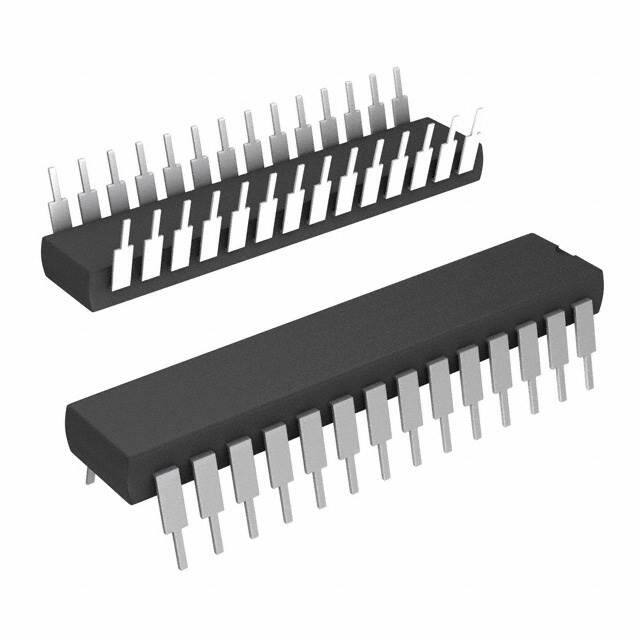
1
Figure 68. 28-Pin DIP Package Diagram
Figure 69. 28-Pin SOIC Package Diagram
DS97DZ80700
PRELIMINARY
8-49
�Z86C83/C84/E83
CMOS Z8® MCU
Zilog
PACKAGE INFORMATION (Continued)
Figure 70. 28-Pin PLCC Package Diagram
8-50
PRELIMINARY
DS97DZ80700
�Z86C83/C84/E83
CMOS Z8® MCU
Zilog
ORDERING INFORMATION
Z86C83
16 MHz
1
Z86E83
16 MHz
28-Pin DIP
28-Pin SOIC
28-Pin PLCC
28-Pin DIP
28-Pin SOIC
28-Pin PLCC
Z86C8316PSC
Z86C8316PEC
Z86C8316SSC
Z86C8316SEC
Z86C8316VSC
Z86C8316VEC
Z86E8316PSC
Z86E8316PEC
Z86E8316SSC
Z86E8316SEC
Z86E8316VSC
Z86E8316VEC
Z86C84
16 MHz
28-Pin DIP
28-Pin SOIC
28-Pin PLCC
Z86C8416PSC
Z86C8416PEC
Z86C8416SSC
Z86C8416SEC
Z86C8416VSC
Z86C8416VEC
For fast results, contact your local Zilog sales office for assistance in ordering the part desired.
CODES
Package
Speed
P = Plastic DIP
S = Plastic SOIC
16 = 16 MHz
Environmental
Temperature
C = Plastic Standard
S = 0°C to + 70°C
E = -40°C to +105°C
Example:
Z 86C83 16 P S C
is a Z86C83, 16 MHz, DIP, 0°C to +70°C, Plastic Standard Flow
Environmental Flow
Temperature
Package
Speed
Product Number
Zilog Prefix
DS97DZ80700
PRELIMINARY
8-51
�Z86C83/C84/E83
CMOS Z8® MCU
Zilog
© 1997 by Zilog, Inc. All rights reserved. No part of this
document may be copied or reproduced in any form or by
any means without the prior written consent of Zilog, Inc.
The information in this document is subject to change
without notice. Devices sold by Zilog, Inc. are covered by
warranty and patent indemnification provisions appearing
in Zilog, Inc. Terms and Conditions of Sale only.
ZILOG, INC. MAKES NO WARRANTY, EXPRESS,
STATUTORY, IMPLIED OR BY DESCRIPTION,
REGARDING THE INFORMATION SET FORTH HEREIN
OR REGARDING THE FREEDOM OF THE DESCRIBED
DEVICES
FROM
INTELLECTUAL
PROPERTY
INFRINGEMENT. ZILOG, INC. MAKES NO WARRANTY
OF MERCHANTABILITY OR FITNESS FOR ANY
PURPOSE.
Zilog, Inc. shall not be responsible for any errors that may
appear in this document. Zilog, Inc. makes no commitment
to update or keep current the information contained in this
document.
Zilog’s products are not authorized for use as critical
components in life support devices or systems unless a
specific written agreement pertaining to such intended use
is executed between the customer and Zilog prior to use.
Life support devices or systems are those which are
intended for surgical implantation into the body, or which
sustains life whose failure to perform, when properly used
in accordance with instructions for use provided in the
labeling, can be reasonably expected to result in
significant injury to the user.
Zilog, Inc. 210 East Hacienda Ave.
Campbell, CA 95008-6600
Telephone (408) 370-8000
FAX 408 370-8056
8-52
PRELIMINARY
DS97DZ80700
�