OB2001
High Performance synchronous rectification controller
GENERAL DESCRIPTION
FEATURES
OB2001 is a high performance and tightly
integrated
secondary
side
synchronous
rectification controller and driver used for
secondary side rectification in switch mode power
supply system. It drivers a much lower voltage
drop N-channel MOSFET to emulate the
traditional diode rectifier at the secondary side of
Flyback converter, which can reduce heat
dissipation, increases output current capability and
efficiency, and simplify thermal design. OB2001
can support low system output voltage down to 2V
at constant current mode.
It is suitable for multiple mode applications
including discontinuous conduction mode and
quasi-resonant mode. With its versatility and
optimization, OB2001 can be used in various
switch mode power supply topologies including
secondary-side control topology and primary-side
control topology.
From the information on the secondary side of the
isolation transformer, OB2001 generates a driving
signal with dead time with respect to the primary
side PWM signal to turn the integrated N-channel
SR switch on and off in proximity of the zero
current transition with the help of smart driver
voltage control. It is optimized for 5V output
voltage.
The externally adjustable minimum on time and
property off time control scheme effectively avoid
the ring impact induced by parasitic elements so
that a reliable and noise free operation of the SR
system is insured.
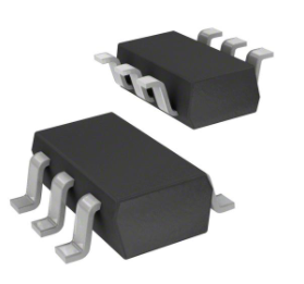
OB2001 is offered in SOT23-6 package.
■
■
■
一
■
■
■
派
■
■
Secondary-side synchronous rectification
controller optimized for 5V output system
Suitable for DCM, QR operation
Accurate secondary side MOSFET Vds
sensing
Low cost small size CC/CV mode support
Up to 200kHz operation frequency
3A/2A peak current sink/source driver
capability
Output voltage overshoot control
VDD UVLO protection
AC/DC 5V adaptors
Cell phone charger
5V Bias supply
Low voltage rectification circuits
Br
ig
ht
co
nf
id
en
tia
■
■
■
■
lt
o
APPLICATIONS
O
n-
TYPICAL APPLICATION
©On-Bright Electronics
Confidential
1
Datasheet
OB_DOC_DS_2001A0
�OB2001
W
O
n-
Br
ig
ht
co
nf
id
en
tia
lt
o
派
一
High Performance synchronous rectification controller
©On-Bright Electronics
Confidential
-2-
Datasheet
OB_DOC_DS_2001A0
�OB2001
W
High Performance synchronous rectification controller
GENERAL INFORMATION
Absolute Maximum Ratings
Parameter
Value
Vin pin
-0.6V to 7V
VDD pin
-0.6V to 7V
VD pin
-2.5V to 50V Note2
Gate pin
-0.6V to 7V
RT pin
-0.6V to 7V
Min/Max
Operating
-40 to 150 ℃
Junction Temperature TJ
Operating
Ambient
-20 to 85 ℃
Temperature TA
Min/Max
Storage
-55 to 150 ℃
Temperature Tstg
Lead
Temperature
260 ℃
(Soldering, 10secs)
lt
o
派
一
Pin Configuration
The OB2001 is offered in SOT23-6 package,
shown as below.
SOT23-6
en
tia
Note1: Stresses beyond those listed under “absolute maximum
ratings” may cause permanent damage to the device. These
are stress ratings only, functional operation of the device at
these or any other conditions beyond those indicated under
“recommended operating conditions” is not implied. Exposure
to absolute maximum-rated conditions for extended periods
may affect device reliability.
Note2: -2.5V applies to minimum duty cycle during normal
operation only.
co
nf
Package Dissipation Rating
Package
RJA(℃/W)
SOT23-6
200
id
Ordering Information
Part Number
Description
OB2001MP
SOT23-6, Pb-free in T&R
X
X
Br
ig
ht
OB2001
Recommended Operating Range
Symbol Parameter
Min/Max
VDD
VDD Supply Voltage
4V to 5.5V
High Performance Synchronous Rectifier
Controller
Package
P:Pb-free
O
n-
M:SOT23-6
Package Pb-free
©On-Bright Electronics
Confidential
3
Datasheet
OB_DOC_DS_2001A0
�OB2001
W
High Performance synchronous rectification controller
Marking Information
en
tia
lt
o
Y:Year Code
WW:Week Code(01-52)
ZZZ: Lot Code
s: Internal Code(Optional)
派
一
001YWW
. ZZZ s
TERMINAL ASSIGNMENTS
I/O
Description
VD
I
This pin is connected to external n-channel MOSFET drain
Gate
O
Driver output for external N-channel MOSFET
GND
P
Ground.
VDD
P
Power Supply
Vin
I
System output voltage detection
RT
O
Minimum on time control pin. A resistor is connected from this pin to GND
O
n-
Br
ig
ht
co
nf
id
Pin Name
©On-Bright Electronics
Confidential
-4-
Datasheet
OB_DOC_DS_2001A0
�OB2001
W
High Performance synchronous rectification controller
O
n-
Br
ig
ht
co
nf
id
en
tia
lt
o
派
一
BLOCK DIAGRAM
©On-Bright Electronics
Confidential
5
Datasheet
OB_DOC_DS_2001A0
�OB2001
W
High Performance synchronous rectification controller
ELECTRICAL CHARACTERISTICS
(TA = 25℃, VDD=5V, unless otherwise noted)
Symbol
Parameter
Test Conditions
Min Typ Max Unit
Supply Voltage (VDD)
1.5
Minimum
Vdd
regulation
voltage
VDD Under Voltage Lockout
UVLO(ON)
Entry
VDD Under Voltage Lockout
UVLO(OFF)
Exit (Recovery)
VD Detection Section
SR MOSFET turn on threshold
Vth_SR_act
voltage detection at VD
SR MOSFET turn off threshold
Vth_SR_deact
voltage detection at Vd
SR
MOSFET
turn-on
Tdelay_on
propagation delay
SR
MOSFET
turn-off
Tdelay_off
propagation delay
0.5
V
2.8 3.0
3.2 V
2.9 3.1
3.3 V
-200
mV
-5
mV
id
100 ns
nf
75
SR MOSFET minimum on time RT=25KΩ
1.9
co
RT Section
Vrt
0.7 mA
4.2
en
tia
lt
o
Vdd_regulation_mini
T_minimum_on
2.0 mA
一
Operation current
派
I_Vdd_operation
Frequency@Vd=65KHz,VD
D=5V,1nF Cap load at
GATE.
Frequency@Vd=2KHz,VDD
=5V,No load at GATE.
Voltage reference at RT pin
0.95 1
n-
Br
ig
ht
Overshoot Control Section
System output 1st overshoot
clamp control trigger voltage at
st
Vo_High_clamp_1
Vin with SR frequency lower
than 7.5KHz
System output 2nd overshoot
nd
Vo_High_clamp_2
clamp control trigger voltage at
Vin
System output overshoot clamp
IVo_High_clamp
current
GATE driver Section
VOH
Output high level @ VDD=5V
VOL
Output low level @ VDD=5V
Pull-up driver
Rds_on
Pull-down driver
Isource
Source current
Isink
Sink current
Us
1.05
V
5.65
V
6.15
V
100
mA
2.5
1.5
2
3
V
V
Ω
Ω
A
A
4.5
O
ns
1
Tf
Falling time
Gate voltage falling from 4V
to 1V @ C L =1nF
30
ns
Tr
Rising time
Gate voltage rising from 1V
to 4V @ C L =1nF
30
ns
©On-Bright Electronics
Confidential
6
Datasheet
OB_DOC_DS_2001A0
�OB2001
W
High Performance synchronous rectification controller
CHARACTERIZATION PLOTS
UVLO(OFF)(V) vs Tem perature
UVLO(ON)(V) vs Tem perature
3.5
3.30
3.10
2.90
2.70
3.1
2.9
2.7
2.5
-40
-10
20
50
80
110 140
-40
-10
VRT(V)
1.03
1.01
0.99
0.97
0.95
50
80
110 140
O
n-
Br
ig
ht
co
nf
Temperature(℃)
140
id
20
110
en
tia
1.05
-10
80
Temperature(℃)
VRT(V) vs Tem perature
-40
50
lt
o
Temperature(℃)
20
派
2.50
3.3
一
UVLO(ON)(V)
UVLO(OFF)(V)
3.50
©On-Bright Electronics
Confidential
7
Datasheet
OB_DOC_DS_2001A0
�OB2001
W
High Performance synchronous rectification controller
Operation Description
OB2001 is a high performance and tightly
integrated
secondary
side
synchronous
rectification controller operating in DCM and QR
mode and driver in switch mode power supply
system. It drivers a much lower voltage drop Nchannel MOSFET to emulate the traditional diode
rectifier, which can reduce heat dissipation,
increases output current capability and efficiency,
and simplify thermal design.
一
Adjustable minimum on time
OB2001 offers adjustable minimum on time
control. This timer can avoid effectively false turnoff due to high frequency interference caused by
parasitic element at the start of secondary-side
demagnetization.
Tonmin=8*RT*10E(-11)
派
Adaptive minimum off time
At the end of demagnetization, SR MOSFET will
be turn off. The remaining current will flow through
body diode again, which may result in negative
voltage (about -700mV) appears at drain and SR
MOSFET will turn on again. In addition, the
resonance oscillation between the magnetization
inductance and parasitic capacitance after
demagnetization may cause negative drain
voltage. These may turn on SR MOSFET by
mistake. To avoid above mis-turn-on of SR
MOSFET, constant minimum off time can be used
to screen it. But it may disturb SR MOSFET
operation. For reliable SR operation, proprietary
adaptive minimum off time control is implemented
in OB2001, which can guarantee reliable
synchronous rectification operation in DCM, QR.
en
tia
lt
o
Startup and under voltage lockout(UVLO)
OB2001 implements UVLO function during startup.
When VDD rises above UVLO(off), the IC wakes
up from under voltage lock out state and enter
normal operation. When VDD drops below
UVLO(on), the IC enter under voltage lock out
state again and the SR gate is pulled low by 10K
resistor on chip. In addition, there is a hysteresis
window between UVLO(off) and UVLO(on) to
make system work reliably.
Br
ig
ht
co
nf
id
Synchronization rectifier
OB2001 controls the turn-on and turn-off of
synchronization rectifier MOSFET (SR MOSFET)
by detection of drain-source voltage. When
demagnetization of transformer starts, the
secondary-side current will flow through the body
diode of SR MOSFET and the voltage at the drain
will drop to about -700mV. As soon as OB2001
detects this negative voltage, the driver voltage is
pulled high to turn on the SR MOSFET after very
short delay time about 100nS, refer to Fig.1.
After the SR MOSFET is turned on, the drain
voltage of SR MOSFET begins to rise based on its
Rdson and secondary-side current. The drain
voltage becomes higher with demagnetization
going on. When the drain voltage rises above 5mV, the driver voltage will be pulled down to
ground very quickly, refer to Fig.1
Gate driver
For good and efficient synchronous rectification
operation, the SR MOSFET should be turned
on/off in very short time. Therefore strong driver
capability is needed. OB2001 can offer typical
source capability 2A and typical sink capability 3A.
This guarantees fast turn-on and turn-off of SR
MOSFET.
n-
Isec
O
Output overshoot clamp
For poor system design, there is usually output
overshoot during startup and load transient. To
facilitate system design, OB2001 can detect
output overshoot condition and prevent overshoot
happen. When output voltage rises to meet the
inner threshold, OB2001 will open a discharge
path from Vin to ground to clamp the system
output voltage, so the system output overshoot
can be prevented.
Vth_SR_deact
Vth_SR_act
Ton_delay
Toff_delay
Fig.1 SR MOSFET turn-on and turn-off timing
©On-Bright Electronics
Confidential
8
Datasheet
OB_DOC_DS_2001A0
�OB2001
W
High Performance synchronous rectification controller
Symbol
ht
co
nf
id
en
tia
lt
o
派
一
PACKAGE MECHANICAL DATA
Dimensions In Millimeters
Max
Min
Max
A
1.000
1.450
0.039
0.057
A1
0.000
0.150
0.000
0.006
A2
0.900
1.300
0.035
0.051
b
0.300
0.500
0.012
0.020
c
0.080
0.220
0.003
0.009
D
2.800
3.020
0.110
0.119
E
1.500
1.726
0.059
0.068
E1
2.600
3.000
0.102
0.118
Br
ig
Min
nO
Dimensions In Inches
e
0.950 (BSC)
0.037 (BSC)
e1
1.800
2.000
0.071
0.079
L
0.300
0.600
0.012
0.024
θ
0º
8º
0º
8º
©On-Bright Electronics
Confidential
9
Datasheet
OB_DOC_DS_2001A0
�OB2001
W
High Performance synchronous rectification controller
IMPORTANT NOTICE
一
RIGHT TO MAKE CHANGES
On-Bright Electronics Corp. reserves the right to make corrections, modifications, enhancements,
improvements and other changes to its products and services at any time and to discontinue any product
or service without notice. Customers should obtain the latest relevant information before placing orders
and should verify that such information is current and complete.
lt
o
派
WARRANTY INFORMATION
On-Bright Electronics Corp. warrants performance of its hardware products to the specifications
applicable at the time of sale in accordance with its standard warranty. Testing and other quality control
techniques are used to the extent it deems necessary to support this warranty. Except where mandated
by government requirements, testing of all parameters of each product is not necessarily performed.
On-Bright Electronics Corp. assumes no liability for application assistance or customer product design.
Customers are responsible for their products and applications using On-Bright’s components, data sheet
and application notes. To minimize the risks associated with customer products and applications,
customers should provide adequate design and operating safeguards.
en
tia
LIFE SUPPORT
On-Bright Electronics Corp.’s products are not designed to be used as components in devices intended to
support or sustain human life. On-bright Electronics Corp. will not be held liable for any damages or
claims resulting from the use of its products in medical applications.
O
n-
Br
ig
ht
co
nf
id
MILITARY
On-Bright Electronics Corp.’s products are not designed for use in military applications. On-Bright
Electronics Corp. will not be held liable for any damages or claims resulting from the use of its products in
military applications.
©On-Bright Electronics
Confidential
10
Datasheet
OB_DOC_DS_2001A0
�