OB2005xK
High Performance synchronous rectifier
GENERAL DESCRIPTION
FEATURES
OB2005xK is a high performance and tightly
integrated secondary side synchronous rectifier for
switch mode power supply system. It combines a
much lower voltage drop N-channel MOSFET to
emulate the traditional diode rectifier at the
secondary side of Flyback converter, which can
reduce heat dissipation, increases output current
capability and efficiency and simplify thermal
design. OB2005xK can support low system output
voltage down to 2V at constant current mode.
It is suitable for multiple mode applications
including discontinuous conduction mode and
quasi-resonant mode. With its versatility and
optimization, OB2005xK can be used in various
switch mode power supply topologies including
secondary-side control topology and primary-side
control topology.
From the information on the secondary side of the
isolation transformer, OB2005xK generates a
driving signal with dead time with respect to the
primary side PWM signal to turn the integrated Nchannel SR switch on and off in proximity of the
zero current transition. It is optimized for 5V output
voltage.
The property minimum off time control scheme
effectively avoid the ring impact induced by
parasitic elements so that a reliable and noise free
operation of the SR system is insured.
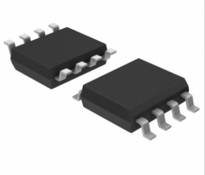
OB2005xK is offered in SOP8 package.
■
Secondary-side
synchronous
rectifier
optimized for 5V output system
■
Suitable for DCM, QR operation
■
Property minimum off time control
■
Accurate
secondary
side
MOSFET
Vds
sensing
■
Low cost small size CC/CV mode support
■
Up to 200kHz operation frequency
■
VDD UVLO protection
APPLICATIONS
■
AC/DC 5V adaptors
■
Cell phone charger
■
5V Bias supply
■
Low voltage rectification circuits
TYPICAL APPLICATION
©On-Bright Electronics
Confidential
1
Preliminary Datasheet
OB_DOC_DS_2005xK00
�OB2005xK
W
High Performance Synchronous Rectifier
GENERAL INFORMATION
Pin Configuration
The OB2005xK is offered in SOP8 package,
shown as below.
Absolute Maximum Ratings
Parameter
Value
Vin pin
-0.6V to 7V
VDD pin
-0.6V to 7V
Drain pin
-0.6V to BVdss Note1
Min/Max
Operating
-40 to 150 ℃
Junction Temperature TJ
Operating
Ambient
-20 to 85 ℃
Temperature TA
Min/Max
Storage
-55 to 150 ℃
Temperature Tstg
Lead
Temperature
260 ℃
(Soldering, 10secs)
Note1: -0.6V is self-clamped
Ordering Information
Part Number
Description
OB2005WKCP
SOP8, Halogen-free in Tube
OB2005WKCPA SOP8, Halogen-free in T&R
OB2005VKCP
SOP8, Halogen-free in Tube
OB2005VKCPA SOP8, Halogen-free in T&R
Recommended Operating Range
Symbol Parameter
Min/Max
VDD
VDD Supply Voltage
4V to 5.5V
Package Dissipation Rating
Package
RJA(℃/W)
SOP8
90
OB2005xK
High Performance Synchronous
Rectifier
©On-Bright Electronics
X
X
X
Package
Green Package
Packing
C:SOP8
P:Halogen-free
Blank:Tube
A: Tape/Reel
Confidential
2
Preliminary Datasheet
OB_DOC_DS_2005xK00
�OB2005xK
W
High Performance Synchronous Rectifier
Marking Information
YWWZZZ
OB2005WCP
K
YWWZZZ
OB2005VCP
K
S
Y:Year Code
WW:Week Code(01-52)
ZZZ:Lot Code
C:SOP8 Package
P:Halogen-free Package
K:Character Code
S:Internal Code(Optional)
S
Y:Year Code
WW:Week Code(01-52)
ZZZ:Lot Code
C:SOP8 Package
P:Halogen-free Package
K:Character Code
S:Internal Code(Optional)
TERMINAL ASSIGNMENTS
Pin Name
GND
Drain
VDD
I/O
P
I/O
P
Vin
I
Description
Ground
SR Mosfet drain pin. This pin is connected to secondary-side winding of transformer
Power Supply
System output voltage detection, 30ohm resistor connected to Vin pin is
recommended
©On-Bright Electronics
Confidential
-3-
Preliminary Datasheet
OB_DOC_DS_2005xK00
�OB2005xK
W
High Performance Synchronous Rectifier
BLOCK DIAGRAM
©On-Bright Electronics
Confidential
4
Preliminary Datasheet
OB_DOC_DS_2005xK00
�OB2005xK
W
High Performance Synchronous Rectifier
ELECTRICAL CHARACTERISTICS
(TA = 25℃, VDD=5V, unless otherwise noted)
Symbol
Parameter
Supply Voltage (VDD)
Test Conditions
I_VDD_operation
Frequency@VD=65KHz,VDD=5V
Frequency@VD=2KHz,VDD=5V
Operation current
VDD_regulation_mini
UVLO(ON)
UVLO(OFF)
Minimum VDD regulation
voltage
VDD Under Voltage Lockout
Entry
VDD Under Voltage Lockout
Exit (Recovery)
Min Typ. Max Unit
1.5 2.0 mA
0.5 0.7 mA
4.2
V
2.8 3.0 3.2 V
2.9 3.1 3.3 V
Drain Section
Vth_SR_act
Vth_SR_deact
Tdelay_on
Tdelay_off
T_minimum_on
SR
MOSFET
turn
on
threshold voltage detection
at Drain
SR
MOSFET
turn
off
threshold voltage detection
at Drain
SR
MOSFET
turn-on
propagation delay
SR
MOSFET
turn-off
propagation delay
SR MOSFET minimum on
time
SR Mosfet Section
Parameter
Product
OB2005WK
OB2005VK
©On-Bright Electronics
-350
mV
-5
mV
100 ns
75
2.1
BVdss(V)
MOSFET Drain-Source Breakdown Voltage
Min
Typ.
Max
40
40
Confidential
5
Rds,on(mΩ)
On resistance
Min
Typ.
13
25
ns
us
Max
Preliminary Datasheet
OB_DOC_DS_2005xK00
�OB2005xK
W
High Performance Synchronous Rectifier
CHARACTERIZATION PLOTS
UVLO(OFF)(V) vs Tem perature
UVLO(ON)(V) vs Tem perature
3.5
UVLO(ON)(V)
UVLO(OFF)(V)
3.50
3.30
3.10
2.90
2.70
2.50
3.3
3.1
2.9
2.7
2.5
-40
-10
20
50
80
110 140
-40
Temperature(℃)
©On-Bright Electronics
-10
20
50
80
110
140
Temperature(℃)
Confidential
6
Preliminary Datasheet
OB_DOC_DS_2005xK00
�OB2005xK
W
High Performance Synchronous Rectifier
Operation Description
OB2005xK is a high performance and versatile
synchronous rectifier. It can emulate the behavior
of Schottky diode rectifier which directly reduces
power dissipation of the traditional rectifiers and
indirectly reduces primary-side loss due to
compounding of efficiency gains.
Adaptive minimum off time
At the end of demagnetization, SR MOSFET will
be turn off. The remaining current will flow through
body diode again, which may result in negative
voltage (about -700mV) appears at drain and SR
MOSFET will turn on again. In addition, the
resonance oscillation between the magnetization
inductance and parasitic capacitance after
demagnetization may cause negative drain
voltage. These may turn on SR MOSFET by
mistake. To avoid above mis-turn-on of SR
MOSFET, constant minimum off time can be used
to screen it. But it may disturb SR MOSFET
operation. For reliable SR operation, proprietary
adaptive minimum off time control is implemented
in OB2005xK, which can guarantee reliable
synchronous rectification operation in DCM, QR.
Startup and under voltage lockout (UVLO)
OB2005xK implements UVLO function during
startup. When VDD rises above UVLO(off), the IC
wakes up from under voltage lock out state and
enter normal operation. When VDD drops below
UVLO(on), the IC enter under voltage lock out
state again and the SR gate is pulled low by 10K
resistor on chip. In addition, there is a hysteresis
window between UVLO(off) and UVLO(on) to
make system work reliably.
Synchronization rectifier
OB2005xK controls the turn-on and turn-off of
synchronization rectifier MOSFET (SR MOSFET)
by detection of drain-source voltage. When
demagnetization of transformer starts, the
secondary-side current will flow through the body
diode of SR MOSFET and the voltage at the drain
will drop to about -700mV. As soon as OB2005xK
detects this negative voltage, the driver voltage is
pulled high to turn on the SR MOSFET after very
short delay time about 100nS, refer to Fig.1.
After the SR MOSFET is turned on, the drain
voltage of SR MOSFET begins to rise based on its
Rdson and secondary-side current. The drain
voltage becomes higher with demagnetization
going on. When the drain voltage rises above 5mV, the driver voltage will be pulled down to
ground very quickly, refer to Fig.1
PCB Layout Consideration
The following rules should be followed in
OB2005Cx PCB Layout:
The Area of Power Loop: The area of the
secondary current loop including the OB2005xK
and the output capacitor should be as small as
possible to reduce EMI radiation. And the PCB
trace must be wide and short for thermal
consideration.
Bypass Capacitor: The bypass capacitor on VDD
should be placed as close as possible to the VDD
pin. And the negative node of VDD capacitor
should be connected directly to the GND pin
(White region as shows in Fig.3).
Isec
Vth_SR_deact
Vth_SR_act
Fig.2 Proper Loop at the Secondary Side of the
Flyback with OB2005xK
Ton_delay
Toff_delay
Fig.1 SR MOSFET turn-on and turn-off timing
Fig.3 Recommend PCB Layout of OB2005xK
©On-Bright Electronics
Confidential
7
Preliminary Datasheet
OB_DOC_DS_2005xK00
�OB2005xK
W
High Performance Synchronous Rectifier
PACKAGE MECHANICAL DATA
SOP8 PACKAGE OUTLINE DIMENSIONS
Dimensions In Millimeters
Dimensions In Inches
Min
Max
Min
Max
A
1.350
1.750
0.053
0.069
A1
0.050
0.250
0.002
0.010
A2
1.250
1.650
0.049
0.065
b
0.310
0.510
0.012
0.020
c
0.100
0.250
0.004
0.010
D
4.700
5.150
0.185
0.203
E
3.800
4.000
0.150
0.157
E1
5.800
6.200
0.228
0.244
e
1.270 (BSC)
L
0.400
1.270
0.016
0.050
θ
0º
8º
0º
8º
Symbol
©On-Bright Electronics
0.050 (BSC)
Confidential
8
Preliminary Datasheet
OB_DOC_DS_2005xK00
�OB2005xK
W
High Performance Synchronous Rectifier
IMPORTANT NOTICE
RIGHT TO MAKE CHANGES
On-Bright Electronics Corp. reserves the right to make corrections, modifications, enhancements,
improvements and other changes to its products and services at any time and to discontinue any product
or service without notice. Customers should obtain the latest relevant information before placing orders
and should verify that such information is current and complete.
WARRANTY INFORMATION
On-Bright Electronics Corp. warrants performance of its hardware products to the specifications
applicable at the time of sale in accordance with its standard warranty. Testing and other quality control
techniques are used to the extent it deems necessary to support this warranty. Except where mandated
by government requirements, testing of all parameters of each product is not necessarily performed.
On-Bright Electronics Corp. assumes no liability for application assistance or customer product design.
Customers are responsible for their products and applications using On-Bright’s components, data sheet
and application notes. To minimize the risks associated with customer products and applications,
customers should provide adequate design and operating safeguards.
LIFE SUPPORT
On-Bright Electronics Corp.’s products are not designed to be used as components in devices intended to
support or sustain human life. On-bright Electronics Corp. will not be held liable for any damages or
claims resulting from the use of its products in medical applications.
MILITARY
On-Bright Electronics Corp.’s products are not designed for use in military applications. On-Bright
Electronics Corp. will not be held liable for any damages or claims resulting from the use of its products in
military applications.
©On-Bright Electronics
Confidential
9
Preliminary Datasheet
OB_DOC_DS_2005xK00
�
很抱歉,暂时无法提供与“OB2005ZKCPA”相匹配的价格&库存,您可以联系我们找货
免费人工找货- 国内价格
- 1+2.62160
- 30+2.53120
- 100+2.35040
- 500+2.16960
- 1000+2.07920