OB2283
High Performance Current Mode PWM Controller
GENERAL DESCRIPTION
FEATURES
OB2283 is a highly integrated current mode PWM
control IC optimized for high performance, low
standby power and cost effective offline flyback
converter applications.
PWM switching frequency at normal operation is
internally fixed and is trimmed to tight range. At no
load or light load condition, the IC operates in
extended ‘burst mode’ to minimize switching loss.
Lower standby power and higher conversion
efficiency is thus achieved.
VCC low startup current and low operating current
contribute to a reliable power on startup and low
standby design with OB2283.
OB2283
offers
comprehensive
protection
coverage with auto-recovery including Cycle-byCycle current limiting (OCP), over load protection
(OLP), and VCC under voltage lockout (UVLO). It
also provides the protections with latched shut
down including over temperature protection (OTP),
and over voltage protection (OVP). Excellent EMI
performance is
achieved
with On-Bright
proprietary frequency shuffling technique.
The tone energy at below 25KHz is minimized in
the design and audio noise is eliminated during
operation.
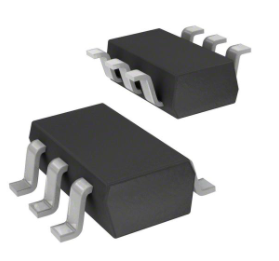
OB2283 is offered in SOT23-6 package.
■
■
■
on
fid
en
tia
lt
o
天
晖
■
■
■
Power on soft start reducing MOSFET Vds
stress
Frequency shuffling for EMI
Extended burst mode control for improved
efficiency and low standby power design
Audio noise free operation
Peak load operation with increased frequency
Comprehensive protection coverage
o VCC Under Voltage Lockout with
hysteresis (UVLO)
o VCC Over Voltage Protection (VCC OVP)
o Cycle-by-cycle over current threshold
setting for constant output power limiting
over universal input voltage range
o Over Load Protection (OLP) with autorecovery
o External (if NTC resistor is connected at
PRT pin)or internal Over Temperature
Protection (OTP) with latched shut down
o Output Over Voltage Protection(Output
OVP) with latched shut down, and the
OVP triggered voltage can be adjusted by
the resistor connected between auxiliary
winding and PRT pin
o Output diode short protection with autorecovery
o GND open protection with auto-recovery
APPLICATIONS
ht
c
Offline AC/DC flyback converter for
■ Printer, Storage power supply
■ Power Adapter
EMI
Filter
DC
Out
O
n-
br
AC IN
ig
TYPICAL APPLICATION
Vaux
OB2283
6 FB
©On-Bright Electronics
VCC 1
5 PRT
CS 2
4 GND
GATE 3
Confidential
-1-
Preliminary Datasheet
OB_DOC_DS_228300
�OB2283
High Performance Current Mode PWM Controller
Absolute Maximum Ratings
Parameter
Value
VCC
1
6
FB
CS
2
5
PRT
Gate
3
GND
4
VCC DC Supply Voltage
VOVP-1V
FB Input Voltage
-0.3 to 7V
CS Input Voltage
-0.3 to 7V
PRT Input Voltage
-0.3 to 7V
Min/Max Operating
Junction Temperature TJ
-40 to 150 ℃
Min/Max Storage
Temperature Tstg
晖
Pin Configuration
-55 to 150 ℃
天
GENERAL INFORMATION
Lead
Temperature
260 ℃
(Soldering, 10secs)
Note: Stresses beyond those listed under
Ordering Information
Part Number
Description
OB2283MP
SOT23-6, Pb-free in T&R
on
fid
en
tia
lt
o
“absolute
maximum ratings” may cause permanent damage to the device.
These are stress ratings only, functional operation of the device
at these or any other conditions beyond those indicated under
“recommended operating conditions” is not implied. Exposure
to absolute maximum-rated conditions for extended periods
may affect device reliability.
Package Dissipation Rating
Package
RJA(℃/W)
SOT23-6
200
Recommended operating condition
Symbol Parameter
Range
VCC
VCC Supply Voltage
12 to 28V
Operating Ambient
TA
-20 to 85 ℃
Temperature
ht
c
OB2283
ig
High Performance Current Mode PWM
Controller
X
Package
M:SOT23-6
X
Package Pb-free
P:Pb-free
O
n-
br
Marking Information
83YWW S
. ZZZ
Y:Year Code
WW:Week Code(01-52)
s: Internal code
ZZZ: Lot code
©On-Bright Electronics
Confidential
-2-
Preliminary Datasheet
OB_DOC_DS_228300
�OB2283
High Performance Current Mode PWM Controller
TERMINAL ASSIGNMENTS
I/O
Description
VCC
P
Power Supply
CS
I
Current sense input
Gate
O
Totem-pole gate driver output for power MOSFET
GND
P
Ground
PRT
I
Dual functions pin. Connecting a NTC resistor to ground for OTP detection.
Connecting a resistor from Vaux can adjust OVP trigger voltage. If both OTP and
OVP are needed, a diode should be connected between PRT pin and the NTC
resistor.
FB
I
Feedback input pin. The PWM duty cycle is determined by voltage level into this pin
and the current-sense signal at Pin CS.
O
n-
br
ig
ht
c
on
fid
en
tia
lt
o
天
晖
Pin Name
©On-Bright Electronics
Confidential
-3-
Preliminary Datasheet
OB_DOC_DS_228300
�OB2283
High Performance Current Mode PWM Controller
FUNCTIONAL BLOCK DIAGRAM
S
Vref&
Iref
AVDD
Diode
short
Internal
blocks
OSC
Diode
short
EX OTP
Vocp
Diode
short
Slope
compensation
OLP
on
fid
en
tia
lt
Temp
sense
OCP
Comparator
晖
R
OVP
GND
open
Soft Driver
天
UVLO
Logic
Control
o
OVP
Q
LEB
AVDD
PWM
Comparator
PK/Green/
Burst
Timer
OLP
OTP
OVP
Latch
O
n-
br
ig
ht
c
EX OVP
©On-Bright Electronics
Confidential
-4-
Preliminary Datasheet
OB_DOC_DS_228300
�OB2283
High Performance Current Mode PWM Controller
ELECTRICAL CHARACTERISTICS
(TA = 25℃, VCC=18V, unless otherwise noted)
Symbol
Parameter
Supply Voltage (VDD)
Operation Current
I_VCC_Burst
Burst Current
VCC Under Voltage Lockout
Enter
VCC Under Voltage Lockout
Exit (Recovery)
Pull-up PMOS active
UVLO(ON)
UVLO(OFF)
ht
c
ig
br
n-
10
uA
2.5
3
mA
mA
7
8
9
V
19
21
23
V
FB=3V,CS=0V. Slowly
VCC Over Voltage Protection
OVP
ramp VCC, until no 29
threshold voltage
gate switching.
Vlatch_release
Latch release voltage
Feedback Input Section(FB Pin)
VFB_Open
VFB Open Loop Voltage
Avcs
PWM input gain ∆VFB/∆VCS
Maximum
duty Max
duty
cycle
@
75
cycle
VCC=18V,VFB=3V,VCS=0V
Vref_green
The threshold enter green mode
Vref_burst_H
The threshold exits burst mode
The threshold enters burst
Vref_burst_L
mode
Short FB pin to GND
IFB_Short
FB pin short circuit current
and measure current
Open loop protection, FB
VTH_OLP
Threshold Voltage
Open loop protection,
Td_OLP
Debounce Time
ZFB_IN
Input Impedance
Current Sense Input(CS Pin)
SST_CS
Soft start time for CS peak
T_blanking
Leading edge blanking time
From Over Current
Over Current Detection and Occurs till the Gate
Td_OC
Control Delay
driver output start to
turn off
Internal
Current
Limiting
VTH_OC
0.43
Threshold Voltage with zero
duty cycle
VTH_OC_Clamp
OCP CS voltage clamper
O
3
0.55 0.65
on
fid
en
tia
lt
Vpull-up
Unit
晖
I_VCC_Operation
VCC=UVLO(OFF)-1V,
measure
leakage
current into VCC
VDD=18V,CS=4V,
FB=3.5V,measure
I(VCC)
CS=0V,FB=0.5V,
measure I(VCC)
Typ Max
天
VCC Start up Current
Min
o
Istartup
Test Conditions
10
30
V
31
V
5
V
5.1
3.5
V
V/V
78
81
%
1.85
1.33
V
V
1.23
V
0.3
mA
4.4
V
15
ms
16
Kohm
4
250
ms
ns
90
ns
0.45 0.47
V
0.69
V
Vdiode_scp
Diode short protection voltage
1.4
V
Td_dio
Diode short debounce time
8
Cycles
©On-Bright Electronics
Confidential
-5-
Preliminary Datasheet
OB_DOC_DS_228300
�OB2283
High Performance Current Mode PWM Controller
Vgnd_open
Td_gnd_open
Td_OCP
GND open protection voltage
difference between GND and
CS
GND
open
protection
debounce time
Over Current protection
debounce Time
0.3
V
20
us
60
ms
100 105
uA
PRT pin
Ioutput_ovp
Td_output_ovp
In-chip OTP
OTP enter
OTP exit
Oscillator
FOSC
Normal Oscillation Frequency
Fosc_PK
Peak frequency
SST_freq
△f_OSC
F_shuffling
Soft start time of frequency
Frequency jittering
Shuffling frequency
Frequency
Temperature
Stability
Frequency Voltage Stability
Burst Mode Switch Frequency
△f_Temp
Output low level @ VDD=18V,
Io=5mA
Output high level @ VCC=18V,
Io=20mA
Output clamp voltage
Output rising time 1.2V ~ 10.8V
@ CL=1000pF
Output falling time 10.8V ~ 1.2V
@ CL=1000pF
ig
VOL
br
VOH
V_clamping
n-
T_r
VDD=18V,FB=3V,
CS=0V
VDD=18V,FB=4.5V,
CS=0V
O
T_f
60
ht
c
△f_VCC
F_Burst
Gate driver
晖
0.95 1
©On-Bright Electronics
1.05
天
Td_OTP
95
o
VOTP
Output current for external OTP
detection
Threshold voltage for external
OTP
External OTP debounce time
Current threshold for adjustable
output OVP
Output OVP debounce time
on
fid
en
tia
lt
IRT
Confidential
-6-
V
5
Cycles
70
uA
5
Cycles
150
120
℃
℃
65
70
KHz
142
KHz
30
+/-6
32
ms
%
Hz
1
%
1
25
%
KHz
1
6
V
V
12
V
160
ns
50
ns
Preliminary Datasheet
OB_DOC_DS_228300
�OB2283
High Performance Current Mode PWM Controller
CHARACTERIZATION PLOTS
VDD = 18V, TA = 25℃ condition applies if not otherwise noted.
UVLO_OFF vs Temperature
8
21
7.8
20.8
7.6
7.4
7.2
20.6
20.4
晖
UVLO_OFF(V)
20.2
20
7
-40
-10
20
50
80
110
-40
140
-10
110
140
o
on
fid
en
tia
lt
Ton_comp (us)
Fosc(KHz)
68
66
64
62
60
-40
-10
20
50
80
110
7.8
7.6
7.4
7.2
7
-40
140
-10
20
50
80
110
140
110
140
110
140
Temperature( ℃)
Temperature( ℃)
V TH_OC vs Tem perature
VOTP vs Tem perature
0.6
ht
c
1.05
1.01
ig
0.99
-10
20
br
0.95
-40
50
80
110
0.54
VTH _OC(V)
1.03
VOTP(V)
80
8
70
0.48
0.42
0.36
0.3
-40
140
-10
50
80
n-
IRT vs Tem perature
OVP vs Tem perature
120
29.6
110
IRT (V)
30
29.2
28.8
100
90
28.4
28
-40
20
Temperature( ℃)
Temperature( ℃)
O
50
Ton_com p vs Tem perature
Fosc vs Tem perature
OVP (V)
20
Tem perature(℃)
Tem perature(℃)
0.97
天
UVLO_ON(V)
UVLO_ON vs Temperature
-10
20
50
80
110
80
-40
140
Temperature( ℃)
©On-Bright Electronics
-10
20
50
80
Temperature( ℃)
Confidential
7
Preliminary Datasheet
OB_DOC_DS_228300
�OB2283
High Performance Current Mode PWM Controller
OPERATION DESCRIPTION
OB2283 is a highly integrated current mode PWM
control IC optimized for high performance, low
standby power and cost effective offline flyback
converter applications. The ‘extended burst mode’
control greatly reduces the standby power
consumption and helps the design easier to meet
the international power conservation requirements.
snubber circuit. The magnitude of power loss is in
proportion to the switching frequency. Lower
switching frequency leads to the reduction on the
power loss and thus conserves the energy.
The switching frequency is internally adjusted at
no load or light load condition. The switch
frequency reduces at light/no load condition to
improve the conversion efficiency. At light load or
no load condition, the FB input drops below
Vref_burst_L (the threshold enter burst mode) and
device enters Burst Mode control. The Gate drive
output switches when FB input rises back to
Vref_burst_H (the threshold exit burst mode).
Otherwise the gate drive remains at off state to
minimize the switching loss and reduces the
standby power consumption to the greatest
extend.
o
天
晖
Startup Current and Start up Control
Startup current of OB2283 is designed to be very
low so that VCC could be charged up above
UVLO threshold level and device starts up quickly.
A large value startup resistor can therefore be
used to minimize the power loss yet achieve a
reliable startup in application.
on
fid
en
tia
lt
Operating Current
The Operating current of OB2283 is low at 2.5mA
(typical). Good efficiency is achieved with OB2283
low operation current together with the ‘extended
burst mode’ control features.
Oscillator Operation
During the full load power operation, OB2283
operates at a 65KHz (typical) fixed frequency. The
efficiency and system cost is controlled at an
optimal level. A peak power mode is implemented
to supply a peak current output requirement. In
peak power mode, frequency is increased from
65KHz (typical) to 142KHz (typical).
At light load levels, OB2283 enters the light load
mode, where the output current is reduced. The
switching losses are reduced by lowering the
switching frequency.
Soft Start
OB2283 features an internal 4ms (typical) soft
start to soften the electrical stress occurring in the
power supply during startup. It is activated during
the power on sequence. As soon as VCC reaches
UVLO(OFF), the CS peak voltage is gradually
increased from 0.05V to the maximum level.
Every restart up is followed by a soft start.
n-
br
ig
ht
c
Frequency shuffling for EMI improvement
The frequency shuffling (switching frequency
modulation) is implemented in OB2283. The
oscillation frequency is modulated so that the tone
energy is spread out. The spread spectrum
minimizes the conduction band EMI and therefore
eases the system design.
O
Current Sensing and Leading Edge
Blanking
Cycle-by-Cycle current limiting is offered in
OB2283 current mode PWM control. The switch
current is detected by a sense resistor into the CS
pin. An internal leading edge blanking circuit
chops off the sensed voltage spike at initial
internal power MOSFET on state due to snubber
diode reverse recovery and surge gate current of
power MOSFET. The current limiting comparator
is disabled and cannot turn off the internal power
MOSFET during the blanking period. The PWM
Extended Burst Mode Operation
At light load or no load condition, most of the
power dissipation in a switching mode power
supply is from switching loss of the MOSFET, the
core loss of the transformer and the loss of the
©On-Bright Electronics
Confidential
8
Preliminary Datasheet
OB_DOC_DS_228300
�OB2283
High Performance Current Mode PWM Controller
duty cycle is determined by the current sense
input voltage and the FB input voltage.
realized through time-division technology as
shown in the figure.
For external OTP detecttion, when switch control
signal S1= “1”, about 20uA (typical) current flows
out from PRT pin. When switch control signal S0=
“1”,about 120uA (typical) current flows out from
PRT pin. The PRT pin voltage difference △Votp
at phase S0 and S1 phase is equal to RT*Iotp.
When △Votp
很抱歉,暂时无法提供与“OB2283MP”相匹配的价格&库存,您可以联系我们找货
免费人工找货- 国内价格
- 1+3.27700
- 30+3.16400
- 100+2.93800
- 500+2.71200
- 1000+2.59900