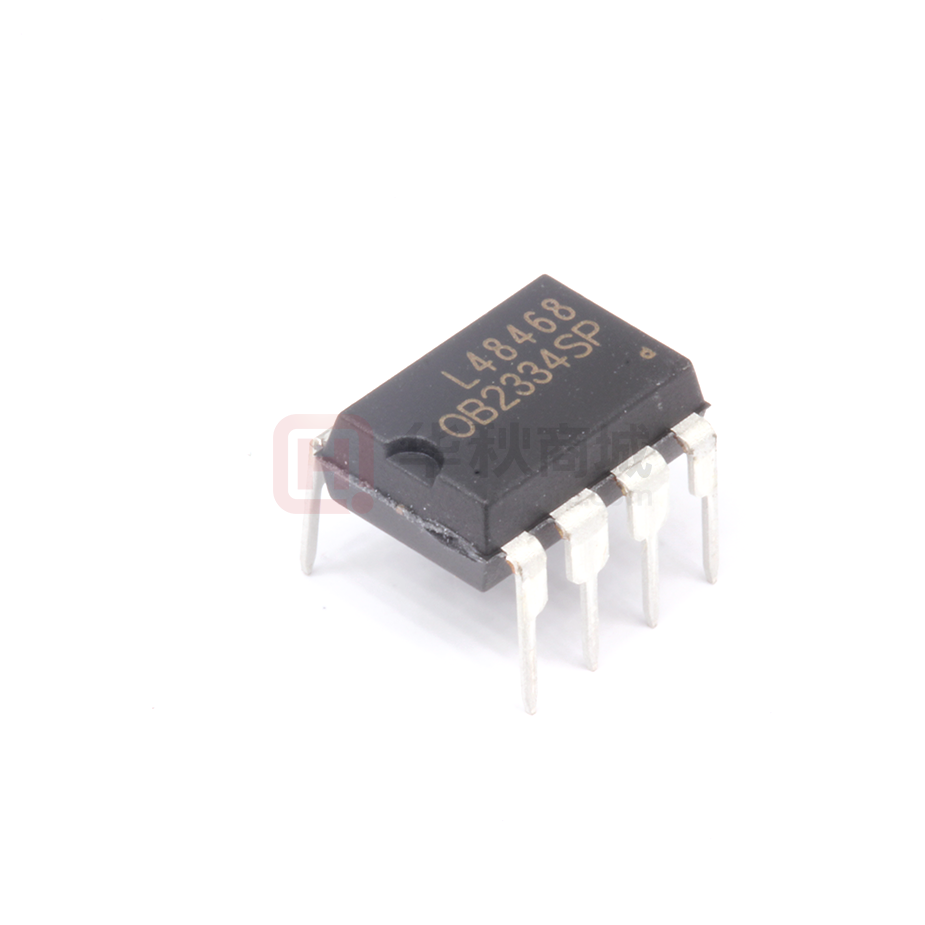
OB2334
High Performance Current Mode PWM Power Switch
GENERAL DESCRIPTION
FEATURES
OB2334 combines a dedicated current mode
PWM controller with a high voltage power
MOSFET. It is optimized for high performance, low
standby power, and cost effective off-line flyback
converter applications in sub 16W range.
OB2334 offers complete protection coverage with
automatic self-recovery feature including Cycleby-Cycle current limiting (OCP), over load
protection (OLP), over temperature protection
(OTP), over voltage protection and VDD under
voltage lockout (UVLO).
Excellent EMI
performance is
achieved
with On-Bright
proprietary frequency shuffling technique together
with soft switching control at the totem pole gate
drive output.
The tone energy at below 20KHZ is minimized in
the design and audio noise is eliminated during
operation.
OB2334 is offered in DIP8 package.
■
lt
o
Level 5 compliance with < 100mW standby
power at universal AC input
■ Power on soft start reducing MOSFET Vds
stress
■ Frequency shuffling for EMI
■ Extended burst mode control for improved
efficiency and minimum standby power design
■ Audio noise free operation
■ Fixed 55KHZ (typical) switching frequency
■ Internal synchronized slope compensation
■ Low VDD startup current and low operating
current
■ Leading edge blanking on current sense input
■ Comprehensive protection coverage
o VDD under voltage lockout with hysteresis
(UVLO)
o Over temperature protection (OTP) with
auto- recovery
o On-Bright
proprietary
line
input
compensated
o Cycle-by-Cycle
over-current
threshold
setting for constant output power limiting
over universal input voltage range.
o Accurate Overload protection (OLP).
o Over voltage protection(OVP)
o Secondary Rectifier Short Protection
EMI
Filter
DC
Out
O
n-
Br
ig
ht
AC IN
co
TYPICAL APPLICATION
nf
id
en
Offline AC/DC flyback converter for
■ AC/DC adapter
■ PDA power supplies
■ Digital Cameras and Camcorder Adapter
■ VCR, SVR, STB, DVD&DVCD Player SMPS
■ Set-Top Box Power
■ Auxiliary Power Supply for PC and Server
■ Open-frame SMPS
tia
APPLICATIONS
OB2334
FB
GND
VDD_G
GND
VDD
Sense
Drain
Drain
Output Power Table
Product
230VAC±15%
Open Frame1
16W
85-265VAC
Open Frame1
11W
OB2334
Notes: 1. Maximum practical continuous power in an open frame design with sufficient drain pattern as a heat sink, at 50℃
ambient. Higher output power is possible with extra added heat sink or air circulation to reduce thermal resistance.
殷先生:133-8036-8939 QQ:71930-7610
-1-
Preliminary Datasheet
OB_DOC_DS_233401
�OB2334
High Performance Current Mode PWM Power Switch
GENERAL INFORMATION
Pin Configuration
The OB2334 is offered in DIP8 package as shown
below.
Package Dissipation Rating
Package
RJA (℃/W)
DIP8
75
Note: Drain Pin Connected to 100mm2 PCB copper clad.
lt
o
Absolute Maximum Ratings
Parameter
Value
Drain Voltage (off state)
-0.3V to BVdss
VDD Voltage
-0.3V to 30 V
VDD-G Input Voltage
-0.3V to 30 V
FB Input Voltage
-0.3 to 7V
Sense Input Voltage
-0.3 to 7V
Min/Max Operating Junction
-40 to 150℃
Temperature TJ
Min/Max Storage
-55 to 150℃
Temperature Tstg
Lead Temperature
260℃
(Soldering, 10secs)
Note: Stresses beyond those listed under “absolute
tia
maximum ratings” may cause permanent damage to the device.
These are stress ratings only, functional operation of the
device at these or any other conditions beyond those indicated
under “recommended operating conditions” is not implied.
Exposure to absolute maximum-rated conditions for extended
periods may affect device reliability.
en
Ordering Information
Part Number
Description
OB2334AP
DIP8, Pb-free
X
X
nf
id
OB2334
Package
A:DIP8
Package Pb-free
P : Pb-free
co
Current Mode PWM Power Switch
O
n-
Br
ig
ht
Marking Information
殷先生:133-8036-8939 QQ:71930-7610
-2-
Preliminary Datasheet
OB_DOC_DS_233401
�OB2334
High Performance Current Mode PWM Power Switch
TERMINAL ASSIGNMENTS
Pin Name
GND
I/O
P
FB
I
VDD-G
SENSE
VDD
P
I
P
Drain
O
Description
Ground
Feedback input pin. The PWM duty cycle is determined by voltage level into this pin
and the current-sense signal at Pin 4.
Internal Gate Driver Power Supply
Current sense input
IC DC power supply Input
HV MOSFET Drain Pin. The Drain pin is connected to the primary lead of the
transformer
BLOCK DIAGRAM
o
VDD_G
3
Current
Reference OTP
Q
S
LDO
OVP
Extended
OSC
Burst mode
id
nf
POR
OCP
SENSE
4
Slope
compensation
CPL
LEB
Vth
co
UVLO
Soft Start
en
R
Power
MOSFET
lt
tia
VDD
2
Internal supply
Soft
Driver
Internal supply
PWM Comparator
Debounce
R
OLP
FB
1
R
7/8 GND
O
n-
Br
ig
ht
Burst
mode
Drain
5/6
殷先生:133-8036-8939 QQ:71930-7610
-3-
Preliminary Datasheet
OB_DOC_DS_233401
�OB2334
High Performance Current Mode PWM Power Switch
ELECTRICAL CHARACTERISTICS
Operation Current
VDD
Under
Voltage
UVLO(ON)
Lockout Enter
VDD
Under
Voltage
UVLO(OFF)
Lockout Exit (Recovery)
Over voltage protection
OVP(ON)
voltage
Feedback Input Section(FB Pin)
VFB_Open
VFB Open Loop Voltage
FB pin short circuit
IFB_Short
current
Zero Duty Cycle FB
VTH_0D
Threshold Voltage
Power Limiting
FB
VTH_PL
Threshold Voltage
Power limiting Debounce
TD_PL
Time
ZFB_IN
Input Impedance
Current Sense Input(Sense Pin)
Soft start time
Leading edge blanking
T_blanking
time
ZSENSE_IN
Input Impedance
CS=0V,FB=3V Ramp up
VDD until gate clock is off
Internal Current Limiting
Threshold Voltage
FB=3.3V
Oscillator
Br
ig
△f_Temp
Normal
Oscillation
Frequency
Frequency Temperature
Stability
Frequency
Voltage
Stability
Maximum duty
cycle
Burst
Mode
Base
Frequency
ht
FOSC
△f_VDD
O
n-
D_max
F_Burst
5
20
uA
mA
9.0
V
15.2
16.2
17.2
V
27.5
29
30.5
V
4.9
5.5
6.1
V
id
VTH_OC
Unit
8.0
nf
Over Current Detection
and Control Delay
co
TD_OC
Max
7.0
Short FB pin to GND and
measure current
From Over Current Occurs
till the gate driver output
start to turn off
Typ
1.6
en
I_VDD_Operation
VDD=11V,Measure
Leakage current into VDD
VFB=3V
o
VDD Start up Current
Min
lt
Istartup
Test Conditions
tia
(TA = 25℃, VDD=16V, unless otherwise noted)
Symbol
Parameter
Supply Voltage (VDD)
0.35
mA
0.8
V
4.6
V
50
mSec
15.7
Kohm
4
ms
270
ns
40
Kohm
80
nSec
0.72
0.77
0.82
V
50
55
60
KHZ
5
%
%
5
FB=3.3V, CS =0V
65
75
85
22
%
KHZ
Mosfet Section
MOSFET Drain-Source
Breakdown Voltage
Static Drain to Source On
Rdson
Resistance
Frequency Shuffling
Frequency
Modulation
∆f_OSC
range /Base frequency
Over temperature protection
Over temperature protection trip point
BVdss
©On-Bright Electronics
600
V
9
-4
150
Confidential
-4-
12
Ώ
4
%
℃
Preliminary Datasheet
OB_DOC_DS_233401
�OB2334
High Performance Current Mode PWM Power Switch
CHARACTERIZATION PLOTS
(The characteristic graphs are normalized at Ta=25℃)
UVLO(ON) vs Temperature
UVLO(OFF) vs Temperature
20
UVLO(OFF) (V)
UVLO(ON)(V)
10
9
8
7
6
18
16
14
12
10
-40
-10
20
50
80
110 140
-40
-10
Temperature(℃ )
80
110 140
o
lt
VDD vs Iop_n(uA)
5
1000
4
tia
800
Iop_n(uA)
3
2
1
600
400
en
I_startup(uA)
50
Temperature(℃ )
I_startup vs Temperature
200
0
-10
20
50
80
110
0
0
co
Duty vs Vth_oc
1
0.9
0.85
Br
ig
0.8
10
20
30
16
20
24
28
45
30
15
0
0.75
0
12
60
ht
0.95
8
Fosc vs Temperature
Fosc(KHz)
1.05
4
VDD(V)
nf
Temperature(℃ )
140
id
-40
Vth_oc(V)
20
40
50
60
-40
70
-10
20
50
80
110
140
Temperature(℃ )
O
n-
Duty(%)
R d so n (o h m )
Rdson(ohm) vs Temperature(℃ )
25.0
20.0
15.0
10.0
5.0
25
50
75
100
Temperature(℃ )
©On-Bright Electronics
125
150
Confidential
-5-
Preliminary Datasheet
OB_DOC_DS_233401
�OB2334
High Performance Current Mode PWM Power Switch
OPERATION DESCRIPTION
The OB2334 is a low power off-line SMPS
Switcher optimized for off-line flyback converter
applications in sub 16W power range. The
‘Extended burst mode’ control greatly reduces the
standby power consumption and helps the design
easily to meet the international power
conservation requirements.
frequency reduces at light/no load condition to
improve the conversion efficiency. At light load or
no load condition, the FB input drops below burst
mode threshold level and device enters Burst
Mode control. The gate drive output switches only
when VDD voltage drops below a preset level and
FB input is active to output an on state. Otherwise
the gate drive remains at off state to minimize the
switching loss and reduces the standby power
consumption to the greatest extend.
The switching frequency control also eliminates
the audio noise at any loading conditions.
Startup Current and Start up Control
Startup current of OB2334 is designed to be very
low so that VDD could be charged up above
UVLO threshold level and device starts up quickly.
A large value startup resistor can therefore be
used to minimize the power loss yet achieve a
reliable startup in application. For AC/DC adapter
with universal input range design, a 2 MΩ, 1/8 W
startup resistor could be used together with a
VDD capacitor to provide a fast startup and yet
low power dissipation design solution.
lt
o
Oscillator Operation
The switching frequency of OB2334 is internally
fixed at 55KHZ. No external frequency setting
components are required for PCB design
simplification.
tia
Current Sensing and Leading Edge Blanking
Cycle-by-Cycle current limiting is offered in
OB2334 current mode PWM control. The switch
current is detected by a sense resistor into the
sense pin. An internal leading edge blanking
circuit chops off the sensed voltage spike at initial
internal power MOSFET on state due to snubber
diode reverse recovery and surge gate current of
internal power MOSFET so that the external RC
filtering on sense input is no longer needed. The
current limiting comparator is disabled and cannot
turn off the internal power MOSFET during the
blanking period. The PWM duty cycle is
determined by the current sense input voltage and
the FB input voltage.
en
Operating Current
The Operating current of OB2334 is low at 1.6mA
(typical). Good efficiency is achieved with OB2334
low operating current together with the ‘Extended
burst mode’ control features.
co
nf
id
Soft Start
OB2334 features an internal 4ms (typical) soft
start to soften the electrical stress occurring in the
power supply during startup. It is activated during
the power on sequence. As soon as VDD reaches
UVLO(OFF), the peak current is gradually
increased from nearly zero to the maximum level
of 0.77V. Every restart up is followed by a soft
start.
ht
Internal Synchronized Slope Compensation
Built-in slope compensation circuit adds voltage
ramp onto the current sense input voltage for
PWM generation. This greatly improves the close
loop stability at CCM and prevents the subharmonic oscillation and thus reduces the output
ripple voltage.
Br
ig
Frequency shuffling for EMI improvement
The frequency Shuffling (switching frequency
modulation) is implemented in OB2334. The
oscillation frequency is modulated so that the tone
energy is spread out. The spread spectrum
minimizes the conduction band EMI and therefore
eases the system design.
O
n-
Driver
The internal power MOSFET in OB2334 is driven
by a dedicated gate driver for power switch control.
Too weak the gate drive strength results in higher
conduction and switch loss of MOSFET while too
strong gate drive results in the compromise of EMI.
Extended Burst Mode Operation
At light load or zero load condition, most of the
power dissipation in a switching mode power
supply is from switching loss on the MOSFET, the
core loss of the transformer and the loss on the
snubber circuit. The magnitude of power loss is in
proportion to the switching frequency. Lower
switching frequency leads to the reduction on the
power loss and thus conserves the energy.
The switching frequency is internally adjusted at
no load or light load condition. The switch
©On-Bright Electronics
A good tradeoff is achieved through the built-in
totem pole gate design with right output strength
and dead time control. The low idle loss and good
EMI system design is easier to achieve with this
dedicated control scheme.
Confidential
-6-
Preliminary Datasheet
OB_DOC_DS_233401
�OB2334
High Performance Current Mode PWM Power Switch
In addition to the gate drive control scheme
mentioned, the gate drive strength can also be
adjusted externally by a resistor connected
between VDD and VDDG, the falling edge of the
Drain output can be well controlled. It provides
great flexibility for system EMI design.
shutdowns the power MOSFET when an Over
Temperature condition is detected or the sense
pin is opened
VDD is supplied by transformer auxiliary winding
output. When VDD voltage exceeds the internal
OVP threshold voltage (29V, typical) due to
abnormal conditions, The power MOSFET is shut
down until VDD drops below 8V (typical) , and
device enters power on restart-up sequence
thereafter.
Protection Controls
Good power supply system reliability is achieved
with its rich protection features including Cycle-byCycle current limiting (OCP), Over Load
Protection (OLP), over voltage protection and
Under Voltage Lockout on VDD (UVLO).
When the secondary rectifier is shorted, the
transformer acts like a leakage inductance.
Meanwhile, the current spike is extremely high.
During high line input, the current in power
MOSFET is too high to wait for OLP delay time. To
offer reliable design, OB2334 shut down the
switcher and enter into auto-recovery mode in this
case.
o
With On-Bright Proprietary technology, the OCP is
line voltage compensated to achieve constant
output power limit over the universal input voltage
range.
O
n-
Br
ig
ht
co
nf
id
en
tia
lt
At overload condition when FB input voltage
exceeds power limit threshold value for more than
TD_PL, control circuit reacts to shut down the
switcher. Switcher restarts when VDD voltage
drops below UVLO limit. Similarly, control circuit
©On-Bright Electronics
Confidential
-7-
Preliminary Datasheet
OB_DOC_DS_233401
�OB2334
High Performance Current Mode PWM Power Switch
PACKAGE MECHANICAL DATA
co
nf
id
en
tia
lt
o
8-Pin Plastic DIP
O
n-
Br
ig
A
A1
A2
B
B1
C
D
E
E1
e
L
E2
Dimensions In Millimeters
Min
Max
3.710
5.334
0.381
2.921
4.953
0.350
0.650
1.524 (BSC)
0.200
0.360
9.000
10.160
6.096
7.112
7.320
8.255
2.540 (BSC)
2.921
3.810
7.620
10.920
ht
Symbol
©On-Bright Electronics
Confidential
-8-
Dimensions In Inches
Min
Max
0.146
0.210
0.015
0.115
0.195
0.014
0.026
0.06 (BSC)
0.008
0.014
0.354
0.400
0.240
0.280
0.288
0.325
0.1 (BSC)
0.115
0.150
0.300
0.430
Preliminary Datasheet
OB_DOC_DS_233401
�OB2334
High Performance Current Mode PWM Power Switch
IMPORTANT NOTICE
RIGHT TO MAKE CHANGES
On-Bright Electronics Corp. reserves the right to make corrections, modifications, enhancements,
improvements, and other changes to its products and services at any time and to discontinue any product
or service without notice. Customers should obtain the latest relevant information before placing orders
and should verify that such information is current and complete.
o
WARRANTY INFORMATION
On-Bright Electronics Corp. warrants performance of its hardware products to the specifications
applicable at the time of sale in accordance with its standard warranty. Testing and other quality control
techniques are used to the extent it deems necessary to support this warranty. Except where mandated
by government requirements, testing of all parameters of each product is not necessarily performed.
On-Bright Electronics Corp. assumes no liability for applications assistance or customer product design.
Customers are responsible for their products and applications using On-Bright’s components, data sheet
and application notes. To minimize the risks associated with customer products and applications,
customers should provide adequate design and operating safeguards.
tia
lt
LIFE SUPPORT
On-Bright Electronics Corp.’s products are not designed to be used as components in devices intended to
support or sustain human life. On-bright Electronics Corp. will not be held liable for any damages or
claims resulting from the use of its products in medical applications.
O
n-
Br
ig
ht
co
nf
id
en
MILITARY
On-Bright Electronics Corp.’s products are not designed for use in military applications. On-Bright
Electronics Corp. will not be held liable for any damages or claims resulting from the use of its products in
military applications.
©On-Bright Electronics
Confidential
-9-
Preliminary Datasheet
OB_DOC_DS_233401
�
很抱歉,暂时无法提供与“OB2334SP”相匹配的价格&库存,您可以联系我们找货
免费人工找货- 国内价格
- 1+1.80235
- 30+1.74020
- 100+1.61590
- 500+1.49160
- 1000+1.42945