OB2560
High Precision CC/CV Primary-Side Controller
GENERAL DESCRIPTION
FEATURES
OB2560 is a high performance offline PSR
controller for low power AC/DC charger and
adapter applications. It operates in primary-side
sensing
and
regulation.
Consequently,
opto-coupler and TL431 could be eliminated.
Proprietary Constant Voltage (CV) and Constant
Current (CC) control is integrated as shown in the
figure below.
In CC control, the current and output power setting
can be adjusted externally by the sense resistor
Rs at CS pin. In CV control, multi-mode operations
are utilized to achieve high performance and high
efficiency. In addition, good load regulation is
achieved by the built-in cable drop compensation.
Device operates in PFM in CC mode at large load
condition and it operates in PWM with frequency
reduction at light/medium load. The chip
consumes very low operation current. It achieves
less than 75mW standby power to meet strict
standby power standard.
OB2560
offers
comprehensive
protection
coverage with auto-recovery feature including
Cycle-by-Cycle current limiting, VDD over voltage
protection, feedback loop open protection, short
circuit protection, built-in leading edge blanking,
VDD under voltage lockout (UVLO), OTP etc.
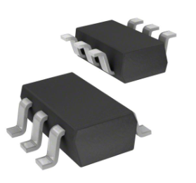
OB2560 is offered in SOT23-6 package.
Driving MOSFET
Primary-side sensing and regulation without
TL431 and opto-coupler
High precision constant voltage and current
regulation at universal AC input
Multi-mode PWM/PFM operation for efficiency
improving
Good dynamic response
Programmable CV and CC regulation
Built-in primary winding inductance
compensation
Programmable cable drop compensation
No need for control loop compensation
Audio noise free operation
Built-in leading edge blanking (LEB)
Ultra low start-up current (typ. 1uA) and low
operating current (typ. 650uA)
Comprehensive protection coverage with
auto-recovery
Precise external OTP
VDD over voltage protection
VDD under voltage lockout with
hysteresis (UVLO)
Cycle-by-Cycle current limiting
Feedback loop open protection
Output short circuit protection
APPLICATIONS
Low Power AC/DC offline SMPS for
Cell Phone Charger
Digital Cameras Charger
Small Power Adapter
Auxiliary Power for PC, TV etc.
Linear Regulator/RCC Replacement
Figure.1. Typical CC/CV Curve
TYPICAL APPLICATION
VO
NS
~
AC
+
+ CO
+
NP
NAUX
FB
VDD
GND
RT
GATE
CS
OB2560
©On-Bright Electronics
+
Confidential
-1-
RS
Datasheet
OB_DOC_DS_2560A0
�OB2560
High Precision CC/CV Primary-Side Controller
Absolute Maximum Ratings
Parameter
Value
VDD Voltage
-0.3 to 30V
FB Input Voltage
-0.3 to 7V
RT Input Voltage
-0.3 to 7V
CS Input Voltage
-0.3 to 7V
GATE Input Voltage
-0.3 to 24V
Min/Max Operating Junction
-40 to 150 ℃
Temperature TJ
Min/Max
Storage
-55 to 150 ℃
Temperature Tstg
Lead
Temperature
260 ℃
(Soldering, 10secs)
Note: Stresses beyond those listed under “absolute maximum
GENERAL INFORMATION
Pin Configuration
The pin map is shown as below for SOT23-6.
ratings” may cause permanent damage to the device. These
are stress ratings only, functional operation of the device at
these or any other conditions beyond those indicated under
“recommended operating conditions” is not implied. Exposure
to absolute maximum-rated conditions for extended periods
may affect device reliability.
Ordering Information
Part Number
Description
OB2560MP
SOT23-6, Pb-free, T&R
Recommended operating condition
Symbol
Parameter
Range
VCC
VCC Supply Voltage
9 to 22V
Operating
Ambient
TA
-20 to 85 ℃
Temperature
Package Dissipation Rating
Package
RθJA (℃/W)
SOT23-6
200
©On-Bright Electronics
Confidential
-2-
Datasheet
OB_DOC_DS_2560A0
�OB2560
High Precision CC/CV Primary-Side Controller
Marking Information
560YWW
. ZZZ s
Y:Year Code
WW:Week Code(01-52)
ZZZ: Lot code
s: Internal code
TERMINAL ASSIGNMENTS
Pin Num
Pin Name
I/O
1
FB
I
The voltage feedback from auxiliary winding. Connected to resistor
divider from auxiliary winding reflecting output voltage.
2
GND
P
Ground
3
RT
I
Connected through a NTC resistor to ground for over temperature
shutdown
4
CS
I
Power MOSFET source
5
GATE
O
Gate driver of power MOSFET.
6
VDD
P
Power Supply
©On-Bright Electronics
Description
Confidential
-3-
Datasheet
OB_DOC_DS_2560A0
�
很抱歉,暂时无法提供与“OB2560MP”相匹配的价格&库存,您可以联系我们找货
免费人工找货- 国内价格
- 5+1.86095
- 50+1.47993
- 150+1.31663
- 500+1.11294
- 3000+1.02222
- 国内价格
- 1+1.18650
- 30+1.14413
- 100+1.10175
- 500+1.01700
- 1000+0.97462
- 2000+0.94920
