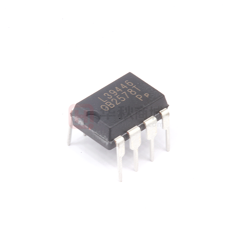
OB2578T
High Performance CCM/QR Mode Primary-Side Power Switch
GENERAL DESCRIPTION
FEATURES
Primary-side sensing and regulation operates
in CCM/QR mode without TL431 and
opto-coupler
High precision constant voltage and current
regulation at universal AC input
Fixed frequency (65kHz) CCM mode
operation with low line voltage at full load
Integrated 4A MOSFET
Quasi-resonant operation for high efficiency in
high line voltage
Programmable CV and CC regulation
Good dynamic response
Built-in line compensation for tight CC
regulation
Built-in fixed cable compensation
Built-in primary winding inductance
compensation
Built-in control loop compensation
Built-in leading edge blanking (LEB)
Ultra low start-up current and low operating
current
Comprehensive protection coverage with
auto-recovery
VDD over voltage protection (VDD OVP)
VDD under voltage lockout with
hysteresis (UVLO)
Cycle-by-cycle current limiting
Feedback open loop protection (OLP)
Output short circuit protection (SCP)
fid
en
tia
lt
o
炜
烨
丰
OB2578T is an excellent primary side regulation
power switch with CC/CV operation for medium
level power AC/DC charger and adapter
applications. The device operates in CCM/QR
mode to provide high efficiency along with several
functions of built-in protections. It removes the
need for secondary feedback circuitry to lower the
total bill of material cost. Proprietary Constant
Voltage (CV) and Constant Current (CC) control is
integrated as shown in the figure below.
In CV control, the controller changes the mode of
operation according to line voltage and load
condition. At full loading, the controller operates in
fixed frequency CCM in low line voltage and
quasi-resonant (QR) mode in high line voltage.
The primary side regulation power supplies up to
high power without the efficiency limitation of DCM
or audible noise.
In CC control, OB2578T samples the primary-side
average current and the demagnetization pulse to
regulation the output current. The current and
output power setting can be adjusted externally by
the sense resistor Rs at CS pin.
OB2578T offers comprehensive protection
coverage with auto-recovery feature including
Cycle-by-Cycle current limiting, VDD OVP, OLP,
SCP, OTP etc.
OB2578T consumes less than 75mW input power
at no-load condition with high line voltage.
OB2578T is offered in SOP8 and DIP8 package.
APPLICATIONS
co
n
Vo
Medium level Power AC/DC offline SMPS for
Cell phone charger
Tablet PC
AC/DC adapter
Set-top box power supplies
ht
±5%
Io
ig
I CC
Br
Figure.1. Typical CC/CV Curve
TYPICAL APPLICATION
O
n-
VO
~
AC
NS
+
C O+
+
NP
+
N AUX
VDD
DRAIN
GND
DRAIN
FB
DRAIN
CS
DRAIN
OB2578T
©On-Bright Electronics
Confidential
-1-
Preliminary Datasheet
OB_DOC_DS_2578T01
�OB2578T
High Performance CCM/QR Mode Primary-Side Power Switch
GENERAL INFORMATION
Pin Configuration
The OB2578T is offered in SOP8 and DIP8
package, shown as below.
DRAIN
GND
2
7
DRAIN
FB
3
6
DRAIN
CS
4
5
DRAIN
丰
8
烨
1
炜
VDD
Absolute Maximum Ratings
Parameter
Value
Drain Voltage (off state)
-0.3V to Bvdss
VDD Voltage
-0.3 to 35V
FB Input Voltage
-0.3 to 7V
CS Input Voltage
-0.3 to 7V
Min/Max Operating Junction
-40 to 150 ℃
Temperature TJ
Operating
Ambient
-20 to 85 ℃
Temperature TA
Min/Max
Storage
-55 to 150 ℃
Temperature Tstg
Lead
Temperature
260 ℃
(Soldering, 10secs)
Note: Stresses beyond those listed under “absolute maximum
Ordering Information
Part Number
Description
SOP8, Halogen-free in Tube
OB2578TCP
OB2578TCPA SOP8, Halogen-free in T&R
OB2578TAP
DIP8, Halogen-free in Tube
o
fid
en
tia
lt
RθJC (℃/W)
25
17
co
n
Package Dissipation Rating
Package
RθJA (℃/W)
SOP-8
85
DIP8
70
ratings” may cause permanent damage to the device. These
are stress ratings only, functional operation of the device at
these or any other conditions beyond those indicated under
“recommended operating conditions” is not implied. Exposure
to absolute maximum-rated conditions for extended periods
may affect device reliability.
ht
OB2578T
90Vac~264Vac Input
OB2578TCP
20W
OB2578TAP
24W
Recommended Operating Condition
Symbol
Parameter
Range
VDD
VDD Supply Voltage
9 to 29V
X
X
X
Package
Green Package
Packing
C:SOP8
A:DIP8
P:Halogen-free
Blank :Tube
A: Tape/Reel
O
n-
Br
ig
High Performance CCM/QR mode
Primary-Side Power Switch
Output Power Table
Product
©On-Bright Electronics
Confidential
-2-
Preliminary Datasheet
OB_DOC_DS_2578T01
�OB2578T
High Performance CCM/QR Mode Primary-Side Power Switch
Marking Information
烨
炜
o
Y:Year Code
WW:Week Code(01-52)
ZZZ:Lot Code
P:Halogen-free Package
S:Internal Code(Optional)
丰
YWWZZZ
OB2578T
Ps
fid
en
tia
lt
TERMINAL ASSIGNMENTS
Pin Name
I/O
Description
1
VDD
P
Power Supply
2
GND
P
Ground
3
FB
I
The voltage feedback from auxiliary winding. Connected to resistor
divider from auxiliary winding reflecting output voltage.
4
CS
I
Current sense input. Connect a sense resistor from this pin to ground.
5~8
DRAIN
I
Drain of power MOS. Connected to input line voltage
O
n-
Br
ig
ht
co
n
Pin Num
©On-Bright Electronics
Confidential
-3-
Preliminary Datasheet
OB_DOC_DS_2578T01
�OB2578T
High Performance CCM/QR Mode Primary-Side Power Switch
BLOCK DIAGRAM
Vref
Reference
OVP &
Open loop
Logic
Vcomp
EA
+
R
CL R
LPF
Q
Vline_os
CV comp
+ CC comp
+
fid
en
tia
lt
Slope
compensation
dem
CC
Control
S/H
LEB
Vref_CC
SC
Filter
CS
dem
O
n-
Br
ig
ht
co
n
GND
Gate
Drive
Q
+
Cable
compensation
Vline_os
Line
compensation
SET
S
丰
CCM/QR
& CV foldback multimode control
dem
sample
Vref_ CV
Drain
Fs_max / Fs_min
烨
Demag
detect
FB
Iref
炜
UVLO&AVDD
o
VDD
©On-Bright Electronics
Confidential
-4-
Preliminary Datasheet
OB_DOC_DS_2578T01
�OB2578T
High Performance CCM/QR Mode Primary-Side Power Switch
ELECTRICAL CHARACTERISTICS
(TA = 25℃, VDD=18V, if not otherwise noted)
Symbol
Parameter
Supply Voltage (VDD) Section
I start-up
Start up current
5
15
uA
0.8
1.0
mA
VDD=UVLO_OFF-1V
FB=1V,
floating
pin
14.5
6.5
31
co
n
fid
en
tia
lt
UVLO(OFF)
VDD under voltage lockout exit
UVLO(ON)
VDD under voltage lockout enter
VDD_OVP
VDD over voltage protection
Current Sense Input Section
TLEB+TD_OC
LEB time and OCP propagation
Vth_ocp_max
Maximum over current threshold
FB Input Section
Reference voltage for feedback
Vref_fb
threshold
V_OVP
Output Over voltage threshold
Vth_cc_shutdown CC mode shut down threshold
CC mode shut down debounce
Tdbs_cc_shutdown
time
Maximum cable compensation
to Vout ratio@Ifb﹥1.02mA
∆cable_max/Vout
Maximum cable compensation
to Vout ratio@Ifb<1.0mA
GATE
2.475
55
Ifb=Vac*1.414*
(Naux/Np)/Rup
Recommended value
Vac=165Vac
@Ifb=1.0mA
1.5
2.5
mA
16
7
33
17.5
7.5
35
V
V
V
520
650
ns
mV
2.5
2.525 V
3.25
1.55
V
V
60
65
ms
2
%
4
190
200
210
mV
60
0.27
65
0.3
70
0.33
kHz
kHz
ig
ht
CC Loop Section
Vref_cc
CC loop reference
Timer Section
Fs_ccm
CV CCM fix frequency
Fmin
Minimum switch frequency
Internal OTP Section
Unit
丰
Operating current
Max
烨
Iop_s
Typ.
炜
Standby current
Min
o
I standy
Test Conditions
internal OTP enter temperature
150
℃
OTP_int_exit
internal OTP exit temperature
120
℃
Br
OTP_int_enter
MOSFET Section
n-
Vds_maxNote
O
Rdson
Mosfet
drain-source
spike
voltage capability
Static drain to source on
resistance
650
V
2.2
Ώ
Note: MOSFET minimum drain to source breakdown voltage is 620V,Voltage spike at not higher than 650V is allowed under the
condition that
A)
Voltage spike duty cycle does NOT exceed 3%
B)
Voltage spike pulse width does NOT exceed 200ns.
©On-Bright Electronics
Confidential
-5-
Preliminary Datasheet
OB_DOC_DS_2578T01
�OB2578T
High Performance CCM/QR Mode Primary-Side Power Switch
CHARACTERIZATION PLOTS
UVLO_ON(V) vs Temperature
17.00
8.00
16.60
7.60
16.20
15.80
15.40
15.00
7.20
6.80
6.40
6.00
-10
20
50
80
110 140
-40
-10
2.560
2.520
o
35.20
Vref_CV(V)
2.600
fid
en
tia
lt
OVP_VCC(V)
110 140
Vref_fb(V) vs Temperature
36.00
32.80
80
Temperature(℃)
VDD_OVP(V) vs Temperature
33.60
50
炜
Temperature(℃)
34.40
20
烨
-40
丰
UVLO_ON(V)
UVLO_OFF(V)
UVLO_OFF(V) vs Temperature
2.480
2.440
32.00
2.400
-40
-10
20
50
80
110 140
-40
20
50
80
110 140
Temperature(℃)
O
n-
Br
ig
ht
co
n
Temperature(℃)
-10
©On-Bright Electronics
Confidential
-6-
Preliminary Datasheet
OB_DOC_DS_2578T01
�OB2578T
High Performance CCM/QR Mode Primary-Side Power Switch
OPERATION DESCRIPTION
炜
烨
丰
CV Mode Operation
OB2578T is designed to produce good CC/CV
control characteristic as shown in the Figure. 1.
In charger applications, a discharged battery
charging starts in the CC portion of the curve until
it is nearly full charged and smoothly switches to
operate in CV portion of the curve. The CC portion
provides output current limiting. In CV operation,
the output voltage is regulated through the primary
side control. In CC operation mode, OB2578T will
regulate the output current constant regardless of
the output voltage drop.
o
Principle of Operation
With OB2578T proprietary CC/CV control, system
can be designed in CCM/DCM mode for flyback
system (Refer to the Typical Application Diagram
in page1).
In the flyback converter, the output voltage can be
sensed via the auxiliary winding. During MOSFET
turn-on time, the load current is supplied from the
output filter capacitor and the current in the
primary winding ramps up. When MOSFET turns
off, the energy stored in the primary winding is
transferred to the secondary side and the current
in the secondary winding is
fid
en
tia
lt
OB2578T is an excellent integrated multi-mode
(see Figure 2) PWM controller optimized for
off-line middle power AC/DC applications. It
operates in continuous conduction mode (CCM)
and quasi-resonant mode (QR) to provide high
efficiency with primary side sensing and regulation
thus provides cost effective solution for energy
efficient power supplies.
At full loading, the IC operates in fixed frequency
(65KHz) CCM mode in the low line input voltage
and it operates in QR mode in high line input
voltage. In this way, high efficiency in the universal
input range at full loading can be achieved.
At normal load condition, it operates in QR mode.
To minimize switching loss, the maximum
switching frequency in QR mode is internally
limited to 80 kHz (typical). When the load goes low,
it operates in PFM mode with valley switching for
high power conversion efficiency. When the load is
very small, the IC switch frequency can be
reduced to 0.3kHz to minimize the standby power
loss. As a result, high conversion efficiency can be
achieved in the whole loading range.
Pulse frequency modulation
(PFM) mode
Frequency
IS
80KHz
co
n
ht
22KHz
300Hz
Vth3
V AUX
N AUX
(VO V )
NS
Sampling Instance
FB
Figure 2 Multi-mode operation diagram
Proprietary built-in CV and CC control can achieve
high precision CC/CV control meeting most
charger application requirements.
Br
VAUX
PWM Off
n-
Startup Current and Start Up Control
Startup current of OB2578T is designed to be very
low so that VDD could be charged up above UVLO
threshold level and device starts up quickly. A
large value startup resistor can therefore be used
to minimize the power loss yet achieve a reliable
startup in application.
O
TDemag
TON
PWM On
Figure.3. Auxiliary winding voltage waveform
Via a resistor divider connected between the
auxiliary winding and FB PIN, the auxiliary voltage
is sampled and hold during the demagnetization
cycle. The sampling instance is variable according
to the demagnetization width. The output voltage
can be monitored when the secondary current is
Operating Current
The Operating current of OB2578T is as low as
around 800uA @ no load mode. Good efficiency
and less than 75mW standby power is achieved
with the low operating current.
©On-Bright Electronics
(2)
Where V indicates the voltage drop of the
output Diode.
Fix Frequency
CCM Mode
ig
Vth1 Vth2
(1)
The auxiliary winding voltage reflects the output
voltage as shown in Figure.3 and it is given by
QR mode
65KHz
NP
IP
NS
Confidential
-7-
Preliminary Datasheet
OB_DOC_DS_2578T01
�OB2578T
High Performance CCM/QR Mode Primary-Side Power Switch
small. Thus ∆V can be ignored. The sampled
voltage is compared with reference voltage Vref_fb
(typical 2.5V) and the difference is amplified. The
error amplifier output reflects the load condition
and controls the switching off time to regulate the
output voltage, thus constant output voltage can
be achieved.
+
FB
Rdw
CS
RS
GND
烨
_
Idw
DRAIN
Figure.5. CC line voltage compensation
(3)
炜
*
VDD
Ifb
CC Mode Operation
OB2578T samples the average CS and the
transformer core demagnetization period to
regulate the output current. The primary average
CS is adaptively controlled according to vref_cc
and the internal CC comp voltage.
Io
N AUX
丰
Rup
Iup
Where Vref_cc (typical 0.2V) is the reference
voltage of CC Loop, Nps is the turn ratio of primary
side to secondary side of the transformer. Rs is the
value of the sense resistor.
Refer to the equation 3, regulating the vref_cc can
achieve the constant output current. The constant
output current is independent of the primary
winding inductance.
fid
en
tia
lt
o
The CS threshold voltage Vcs is given by
1 Naux
Ros (5)
Vcs Vth _ cc
2 Vac
M Np
Rup
Where Vth_cc a threshold determined by internal
CC comp voltage, M is the FB current mirror ratio
(M=430), Naux/Np is the auxiliary winding to
primary winding turns ratio, Vac is the effective
voltage of input voltage, Ros is the internal line
compensation offset resistor (Ros=1.5kohm) , Rup
is the external FB PIN upside resistor.
Adjustable CC Point and Output Power
In OB2578T, the CC point and maximum output
power can be externally adjusted by external
current sense resistor Rs at CS pin as illustrated in
the typical application diagram. The larger the Rs
is, the smaller CC point is, and the smaller output
power becomes, and vice versa as shown in
Figure.4.
co
n
Current Sensing and Leading Edge Blanking
Cycle-by-Cycle current limiting is offered in
OB2578T. The switch current is detected by a
sense resistor connected to the CS pin. An internal
leading edge blanking circuit chops off the sensed
voltage spike at initial power MOSFET on state so
that the external RC filtering on sense input is no
longer needed.
Vo
Br
ig
ht
Large Rs
Internal Over-Temperature Protection with
GATE Shutdown
The internal OTP circuit of OB2578T is triggered
and only shuts down the internal MOSFET when
the chip temperature rises above 150℃, and the
internal MOSFET will resume switching after the
chip temperature falls below 120℃.
Small Rs
Io
Protection Control
Good power supply system reliability is achieved
with its rich protection features including
Cycle-by-Cycle current limiting, Output over
voltage protection, VDD over voltage protection,
short circuit protection, Under Voltage Lockout on
VDD.
VDD is supplied by transformer auxiliary winding
output after startup. The output of OB2578T is shut
down when VDD drops below UVLO (ON) and the
power converter enters power on start-up
sequence thereafter.
n-
Figure.4. Adjustable output power by changing Rs
O
CC Line Voltage Compensation
The variation of maximum output current in CC
mode can be rather large at high input voltage
(such as 264Vac) if no compensation is provided.
The CC threshold value is self adjusted higher at
higher AC voltage due to CC propagation delay. In
OB2578T, the AC line voltage information is
sampled through detecting FB sourcing current
when gate turns on, and the AC line voltage
information is added to the CS pin voltage. So the
maximum CS threshold voltage Vcs_max in
OB2578T is a function of the CC threshold and AC
line voltage information as shown in Figure 5.
©On-Bright Electronics
CC mode shutdown function
In OB2578T, to prevent the controller operating
Confidential
-8-
Preliminary Datasheet
OB_DOC_DS_2578T01
�OB2578T
High Performance CCM/QR Mode Primary-Side Power Switch
under abnormal conditions, the minimum output
voltage of CC mode is limited to predetermined
voltage. The CC output voltage is sampled through
FB pin from auxiliary winding at the middle of the
de-magnetization. When the FB sampled voltage
is below 1.55V and last 60ms, the controller will
shut down.
rectifying loop (Red wire as shows in Fig.6).
Bypass Capacitor and FB Divider Resistor: The
bypass capacitor on VDD and the FB divider
resistor should be placed as close as possible to
pin out. And the negative node of VDD capacitor
and the FB down resistor should be connected
directly to the IC GND pin before single point
connected to the negative node of the output
capacitor. (Blue wire as shows in Fig.6)
Ground Path: The GND path of the input power
loop and IC controller path should be separated
and connected at the negative terminal of input
capacitor by single point, such as power sense
resistor, the negative of the auxiliary winding and
the IC GND.
炜
烨
丰
PCB Layout Consideration
The following rules should be followed in OB2578T
PCB Layout:
The Area of Power Loop: The area of the main
current loop should be as small as possible to
reduce EMI radiation, such as the primary current
loop, the snubber circuit and the secondary
o
NP
~
AC
+ CO
fid
en
tia
lt
NS
VO
+
+
+
NAUX
VDD
Drain
GND
Drain
FB
Drain
CS
Drain
OB2578T
co
n
RS
O
n-
Br
ig
ht
Fig.6 Fly-back Schematic with OB2578T
Fig.7 Recommend PCB Layout of OB2578T
©On-Bright Electronics
Confidential
-9-
Preliminary Datasheet
OB_DOC_DS_2578T01
�OB2578T
High Performance CCM/QR Mode Primary-Side Power Switch
ig
ht
co
n
fid
en
tia
lt
o
炜
烨
丰
PACKAGE MECHANICAL DATA
Symbol
O
n-
Br
A
A1
A2
b
c
D
E
E1
e
L
θ
©On-Bright Electronics
Dimensions In Millimeters
Min
Max
1.350
1.750
0.050
0.250
1.250
1.650
0.310
0.510
0.170
0.250
4.700
5.150
3.800
4.000
5.800
6.200
1.270 (BSC)
0.400
1.270
0º
8º
Confidential
- 10 -
Dimensions In Inches
Min
Max
0.053
0.069
0.002
0.010
0.049
0.065
0.012
0.020
0.006
0.010
0.185
0.203
0.150
0.157
0.228
0.244
0.05 (BSC)
0.016
0.050
0º
8º
Preliminary Datasheet
OB_DOC_DS_2578T01
�OB2578T
High Performance CCM/QR Mode Primary-Side Power Switch
O
n-
Br
A
A1
A2
B
B1
C
D
E
E1
e
L
E2
Dimensions In Millimeters
Min
Max
3.710
5.334
0.381
2.921
4.953
0.350
0.650
1.524 (BSC)
0.200
0.360
9.000
10.160
6.096
7.112
7.320
8.255
2.540 (BSC)
2.921
3.810
7.620
10.920
ig
Symbol
ht
co
n
fid
en
tia
lt
o
炜
烨
丰
PACKAGE MECHANICAL DATA
©On-Bright Electronics
Confidential
- 11 -
Dimensions In Inches
Min
Max
0.146
0.210
0.015
0.115
0.195
0.014
0.026
0.06 (BSC)
0.008
0.014
0.354
0.400
0.240
0.280
0.288
0.325
0.1 (BSC)
0.115
0.150
0.300
0.430
Preliminary Datasheet
OB_DOC_DS_2578T01
�OB2578T
High Performance CCM/QR Mode Primary-Side Power Switch
IMPORTANT NOTICE
RIGHT TO MAKE CHANGES
On-Bright Electronics Corp. reserves the right to make corrections, modifications, enhancements,
improvements and other changes to its products and services at any time and to discontinue any product
or service without notice. Customers should obtain the latest relevant information before placing orders
and should verify that such information is current and complete.
炜
烨
丰
WARRANTY INFORMATION
On-Bright Electronics Corp. warrants performance of its hardware products to the specifications applicable
at the time of sale in accordance with its standard warranty. Testing and other quality control techniques
are used to the extent it deems necessary to support this warranty. Except where mandated by
government requirements, testing of all parameters of each product is not necessarily performed.
On-Bright Electronics Corp. assumes no liability for application assistance or customer product design.
Customers are responsible for their products and applications using On-Bright’s components, data sheet
and application notes. To minimize the risks associated with customer products and applications,
customers should provide adequate design and operating safeguards.
fid
en
tia
lt
o
LIFE SUPPORT
On-Bright Electronics Corp.’s products are not designed to be used as components in devices intended to
support or sustain human life. On-bright Electronics Corp. will not be held liable for any damages or claims
resulting from the use of its products in medical applications.
O
n-
Br
ig
ht
co
n
MILITARY
On-Bright Electronics Corp.’s products are not designed for use in military applications. On-Bright
Electronics Corp. will not be held liable for any damages or claims resulting from the use of its products in
military applications.
©On-Bright Electronics
Confidential
- 12 -
Preliminary Datasheet
OB_DOC_DS_2578T01
�