OB2603x
Secondary-side CV/CC controller
with QC3.0& PE+2.0 Protocol
FEATURES
The OB2603x is a highly integrated secondary
-side constant voltage and constant current
(CV/CC) controller supporting both Qualcomm
Quick Charge QC3.0 protocol and Media Tek
Pump Express Plus 2.0 PE+2.0 protocol. It is used
in application that requires constant voltage (CV)
and constant current (CC) regulation. Two
operational amplifiers are built in for voltage loop
(CV) and current loop (CC) regulation with
programmable voltage reference to provide
adaptive CV and CC in high precision. The high
gain current sense amplifier minimizes the offset
for decreasing power loss of sense resistor.
The OB2603x automatically detects QC3.0 or
PE+2.0 or BC1.2 and enables output voltage
adjustments accordingly. It supports the multi-level
output voltage range from 3.6V to 12V in 0.2V
increments for QC3.0 protocol. And it provides the
output voltage from 5V to 9V in 0.5V increments
and 12V voltage for MTK PE+2.0 protocol. If quick
charge protocol is not detected, the OB2603x
disables the output voltage adjustment to ensure
safe operation with default 5V output voltage. I-V
curve is shown in Figure 1.
OB2603x can achieve lower standby power
consumption and fast voltage transition while
TM
works together with On-Bright GreenEngine
based AC/DC off-line PWM ICs.
The OB2603x offers comprehensive protection
coverage including constant current limiting, over
voltage protection at different output voltage levels
and under voltage protection.
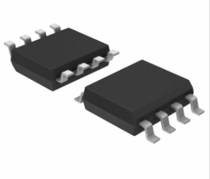
OB2603x is offered in SOP8 package.
Protocol Support
USB BC 1.0&1.2
Qualcomm Quick Charge 2.0 & 3.0
(QC2.0 & QC3.0)
Media Tek Pump Express 1.0& 2.0
(PE+1.0 & PE+2.0)
Automatic Identification of Protocols
Highly Integration
Secondary—Side Constant Voltage
(CV)and Constant Current (CC)
Regualtion
Built-in Two Operational Amplifiers for
Dual CV/CC control
Built-in Unplug Fast Discharging Control
Programmable Cable Drop Compensation
Built-in opto-coupler driver
Support 18W and 24W constant power
Low Operating Current
Wide operation voltage range from 3V to 12V.
Comprehensive protection coverage
Output over voltage protection(OVP)
Output under voltage protection(UVP)
Internal over temperature protection
(OTP)
co
nf
id
en
tia
lt
o
派
一
GENERAL DESCRIPTION
APPLICATIONS
O
n-
Br
ig
ht
Quick-charging AC/DC charges for cell
phones, tablets and other portable devices
AC/DC Adapters for Portable Devices that
Requires CV/CC control
Figure1. Typical I-V Curve
©On-Bright Electronics
Confidential
-1-
Preliminary datasheet
OB_DOC_DS_2603x01
�OB2603x
Secondary-side CV/CC controller with QC3.0& PE+2.0 Protocol
en
tia
lt
o
派
一
TYPICAL APPLICATION
O
n-
Br
ig
ht
co
nf
id
Note: Using GreenEngineTM as Primary-Side Controller
©On-Bright Electronics
Confidential
-2-
Preliminary datasheet
OB_DOC_DS_2603x01
�OB2603x
Secondary-side CV/CC controller with QC3.0& PE+2.0 Protocol
GENERAL INFORMATION
8
DP
GND
2
7
DN
VIN
3
6
VFB
IFB
4
5
OPTO
派
1
lt
o
ISP
Absolute Maximum Ratings
Parameter
Value
ISP/DP/DN/IFB/RT Voltage
-0.3 to 7V
VIN/VFB/OPTO Voltage
-0.3 to 30V
Min/Max Operating Junction
-40 to 150 ℃
Temperature TJ
Operating Ambient Temperature
-20 to 85 ℃
TA
Min/Max Storage Temperature
-55 to 150 ℃
Tstg
Lead Temperature (Soldering,
260 ℃
10secs)
Note: Stresses beyond those listed under “absolute maximum
一
Pin Configuration
The pin map is shown as below for SOP8
ratings” may cause permanent damage to the device. These
are stress ratings only, functional operation of the device at
these or any other conditions beyond those indicated under
“recommended operating conditions” is not implied. Exposure
to absolute maximum-rated conditions for extended periods
may affect device reliability.
id
Recommended operating condition
Symbol
Parameter
Range
VIN
VIN Supply Voltage
3 to 25V
Recommended output power
Product
OB2603A
24W
OB2603B
18W
O
n-
Br
ig
ht
co
nf
Package Dissipation Rating
Package
RθJA (℃/W)
SOP-8
150
en
tia
Ordering Information
Part Number
Description
OB2603ACP
SOP8, Halogen-free in Tube
OB2603ACPA
SOP8, Halogen-free in T&R
OB2603BCP
SOP8, Halogen-free in Tube
OB2603BCPA
SOP8, Halogen-free in T&R
©On-Bright Electronics
Confidential
-3-
Preliminary datasheet
OB_DOC_DS_2603x01
�OB2603x
Secondary-side CV/CC controller with QC3.0& PE+2.0 Protocol
YWWZZZ
OB2603CP
B
TERMINAL ASSIGNMENTS
Y:Year Code
WW:Week Code(01-52)
ZZZ:Lot Code
C:SOP8 Package
P:Halogen-free Package
B:Character Code
S:Internal Code(Optional)
lt
o
Y:Year Code
WW:Week Code(01-52)
ZZZ:Lot Code
C:SOP8 Package
P:Halogen-free Package
A:Character Code
S:Internal Code(Optional)
Pin Name
I/O
Description
1
ISP
I
Output current sensor (positive)
2
GND
I
3
VIN
4
IFB
5
OPTO
nf
id
Pin Num
co
GND (Output current sensor (negative))
Output voltage sensor and discharger
I
Output current feedback input
Br
ig
ht
I
I
Opto driver
6
VFB
I
Output voltage feedback input
7
DN
I
D- signal of USB
8
DP
I
D+ signal of USB
O
n-
S
派
S
en
tia
YWWZZZ
OB2603CP
A
一
Marking Information
©On-Bright Electronics
Confidential
-4-
Preliminary datasheet
OB_DOC_DS_2603x01
�OB2603x
Secondary-side CV/CC controller with QC3.0& PE+2.0 Protocol
BLOCK DIAGRAM
DP/DN
Input
Oscillator
OPTO
V
CLK
I Vref_cv_cc
一
DP
DN
IFB
Cable
Compensation
-
CV_EA
OVP
detector
UVP
detector
Vin
Idis
OVP
dis_ctrl
Vref_CC
lt
o
Discharge
detector
派
+
Digital
control
Dis_end
UVP
-
CC_EA
+
GND
Ovp_blank
VIN
PG
UVLO/LDO
AVCCR
ISP
+
-
GND
IFB
Reference
+
comp
-
Vref_load_det
O
n-
Br
ig
ht
co
nf
id
R
AVDD
en
tia
Mtk_in
5R
Vsense
VFB
©On-Bright Electronics
Confidential
-5-
Preliminary datasheet
OB_DOC_DS_2603x01
�OB2603x
Secondary-side CV/CC controller with QC3.0& PE+2.0 Protocol
ELECTRICAL CHARACTERISTICS
(TA = 25℃, if not otherwise noted)
Symbol
Parameter
Supply Voltage (VIN) Section
Test Conditions
I start-up
Start-up Current
VIN=2V
0.5
mA
I ops
Standby operation current
VIN=5V
1
mA
UVLO(OFF)
Start-up threshold
VIN rising
3.0
V
UVLO(ON)
Undervoltage lockout threshold
VIN falling
2.65
V
Class A wall adapter range
Vbus_cont_step
Voltage tolerance per step in
continuous mode
Vslew
Maximum slew rate on Vbus
Vdat_ref
Date detect voltage
Vsel_ref
Max
一
3.6
lt
o
Vbus_cont_range
Typ.
派
Quick charge Section (DP/DN pin)
Min
Unit
12
V
0.2
0.25
V
-
-
30
mV/us
0.25 0.325
0.4
V
Output voltage selection reference
1.8
2
2.2
V
Rdat_lkg
DP data line leakage resistance
300
450
600
KΩ
RDCP_dat
DP\DN short resistance
15
25
Ω
RDM-DWM
DN pull down resistance
14.25 19.53 24.80
Tglitch_bc_done
DP high glitch filter time
1
1.25
Tglitch_dm_low
DN low glitch filter time
1
1.4
ms
Tglitch__dm_high
DN high glitch filter time
40
60
ms
Tglitch _v_change
40
id
nf
unplug glitch filter time
20
25
30
ms
20
40
60
ms
100
200
us
0.2
15
ms
New voltage request time
Glitch filter on voltage mode
requests
Rising and falling edge glitch filter
on pulses in continuous
Active pulse time in continuous
mode
Time
between
pulses
in
continuous mode
Time for an HVDCP change its
output voltage to within Vbus_5V
or Vbus_HV from the voltage
mode request is made
Time HVDCP must allow VBUS to
collapse below the threshold
Time for VBUS to discharge to
VBUS_5V when DP goes below
Vdat_vref
Time for VBUS to discharge to
VBUS_5V when DP goes below
Vdat_vref for a USB type-c ouput
Br
ig
Tglitch_mode_change
Tglitch_cont_change
n-
Tactive
O
Tinactive
TV_cont_change
Tglitch_UVLO
TV_unplug
TV_unplug_C
S
co
Tunplug
1.5
kΩ
20
output voltage glitch filter time
ht
Tv_new_request
en
tia
0.15
©On-Bright Electronics
Confidential
-6-
60
ms
200
ms
200
-
us
2
60
20
ms
ms
500
ms
275
ms
Preliminary datasheet
OB_DOC_DS_2603x01
�OB2603x
Secondary-side CV/CC controller with QC3.0& PE+2.0 Protocol
maximumu discharge time
I_dis
Mirror discharge current
VIN
很抱歉,暂时无法提供与“OB2603BCPA”相匹配的价格&库存,您可以联系我们找货
免费人工找货- 国内价格
- 1+1.39272
- 30+1.34470
- 100+1.29668
- 500+1.20063
- 1000+1.15260
- 2000+1.12379