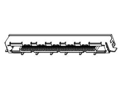
THD-LVDSSeries ▓Pitch=0.5mm Wafer Connector (Front–Flip lower contact)
Product Specification
深圳市臺華達科技有限公司
S H E N Z H E N S H I TH D Electronics Co., Ltd.
Product.No
THD-LVDS-51R-GF
Pitch=0.5mm
A
Release
Rev.
Description
■Prepared By
■Checked By
■Approved By
Wafer Connector (Front–Flip Lower Contact)
Approved Signatures
:
JIM
:
JIM
:
黄德进
■Date:
■Date:
■Date:
1/3
2012.05.24
2012.05.24
2012.05.24
�THD-LVDSSeries ▓Pitch=0.5mm Wafer Connector (Front–Flip lower contact)
■Scope
This specification covers the 1.O mm Pitch Wafer Connector THDLVDS series.
■Ordering information
THDLVDS - 51 R - GF
❶
❷
❸
❶
Series name:THDLVDS
❷
Number of contacts:51
❸
PIN
■Rating
❹
❹
Plating:
GF= 1µ”~3µ” Gold Flash
G3= 3µ” Gold over Nickel
G5= 5µ” Gold over Nickel
SN= Tin(Lead Free) over Nickel
Item
Standard
Voltage Rating(Max.)
200V AC
Current Rating(Max.)
1.0A DC
Operating Temperature Range
■Material
Housing
L.C.P (UL94V-0)
Actuator
L.C.P
(UL94V-0)
-55°C ~ +85°C (Including terminal temperature rise)
Terminal
Solder pin
SHELL
Copper alloy
Copper alloy
Copper alloyl
■Performance
Item
Test Condition
Specification
Mate applicable FPC and measure by dry circuit, 20mV
40 mΩ Max.
Max, 1mA.
Mate applicable FPC and apply 500V DC between adjacent
Insulation Resistance
100 MΩ Min.
terminal or ground.
Mate applicable FPC, apply 250V AC(rms) for
Dielectric Strength
No Breakdown
1 minute between adjacent terminal or ground.
Insert the actuator, pull the FPC at a rate of 25±3mm
FPC Retention Force
Per pin x 2N MAX.
per minute.
Terminal Retention
Apply axial pull out force at the rate of 25±3 mm/minute
Per pin x 0.15Kgf {1.5N} Min.
Force
on the terminal assembled in the housing.
Mate connectors and subject to the following vibration
Appearance
No Damage
conditions, for period of 2 hours in each of 3 mutually
perpendicular axes, passing DC 1mA during the test.
Contact
100 mΩ Max.
Vibration
Resistance
Amplitude : 1.5mm P-P
Frequency : 10~55~10 Hz in 1 minute.
Discontinuity
1 μsec Max.
Duration : 2 hours in each of X,Y,Z axes.
Mate applicable FPC and subject to the following shock
Appearance
No Damage
conditions. 3 times of shocks shall be applied for each
Contact
6 directions along 3 mutually perpendicular axes,
100 mΩ Max.
Shock
Resistance
passing DC 1 mA current during the test.
Contact Resistance
Salt Spray
Peak value : 490m/s2 {50G}
Mate applicable FPC and expose to the following salt
mist conditions. Upon completion of the exposure
period, salt deposits shall be removed by a gentle wash
or dip in running water, after which the specified
measurements shall be performed.
NaCl solution
Concentration
: 5 ± 1%
Spray time
:48 ± 4 hours
Ambient temperature : 35 ± 2°C
2/3
Discontinuity
1 μsec Max.
Appearance
No Damage
Contact
Resistance
100 mΩ Max.
�THD-LVDSSeries ▓Pitch=0.5mm Wafer Connector (Front–Flip lower contact)
Item
Test Condition
Heat Resistance
Cold Resistance
Specification
Mate applicable FPC and expose to 85±2°C for 96 hours.
Upon completion of the exposure period, the test
specimens shall be conditioned at ambient room
conditions for 1 to 2 hours, after which the specified
measurements shall be performed.
Mate applicable FPC and expose to -40±2°C for 96 hours.
Upon completion of the exposure period, the test
specimens shall be conditioned at ambient room
conditions for 1 to 2 hours, after which the specified
measurements shall be performed.
Mate applicable FPC and expose to 60 ± 2°C, relative
humidity 90 to 95% for 96 hours. Upon completion of
the exposure period, the test specimens shall be
conditioned at ambient room conditions for 1 to 2
hours, after which the specified measurements shall
be performed.
Humidity
Temperature Rise
Mate applicable FPC and measure the temperature rise
of contact when the maximum AC rated current is passed.
Temperature Cycling
Mate applicable FPC and subject to the following
conditions for 5 cycles.
Upon completion of the exposure period, the test
specimens shall be conditioned at ambient room
conditions for 1 to 2 hours, after which the specified
measurements shall be performed.
1 cycle
a) -55±3°C
30minutes
b) +85±3°C
30minutes
(Transit time shall be with in 3 minutes)
Solderability
Tip of solder tails and fitting nails into the molten
solder (held at 245±5°C) up to 0.1mm from the bottom
of the housing for 3±0.5 seconds.
When reflowing refer to Infrared reflow condition
Soldering iron method
Resistance to Soldering 0.2mm from terminal tip and fitting nail tip.
Soldering time
: 5 seconds Max.
Solder temperature : 370~400°C
■Recommended Temperature Profile
250°C MAX(Peak Temp)3sec or less
230°C MIN/20~40sec
(60sec)
Start (Pre-Heat 150°C MAX)
(60~90sec)
(30sec)
Emperature Condition Graph
(Temperature On Board Pattern Side)
3/3
Appearance
No Damage
Contact
Resistance
100 mΩ Max.
Appearance
No Damage
Contact
Resistance
100 mΩ Max.
Appearance
No Damage
Contact
Resistance
100 mΩ Max.
Dielectric
Strength
No Breakdown
Insulation
Resistance
50 MΩ Min.
Temperature
rise
30°C Max.
Appearance
No Damage
Contact
Resistance
100 mΩ Max.
Solder
Wetting
95% of immersed
area must show no
voids, pin holes.
Appearance
No Damage
�NO.OF
PIN
DIMENSION
A±0.15
B±0.15 C±0.15 D±0.15
E±0.1
F±0.1
G+0.10
0.00
H±0.15
I
J
51
37.8 35.35 31.00 25.00 5.00 25.00 32.65 25.00 35.95 34.75
41
32.8 30.35 26.00 20.00 4.00 20.00 28.65 20.00 30.95 29.75
HOUSING
SHELL
镍底
雾锡
镍底
半金雾锡
TERMINAL
深 圳 市 台 华 达 科 技 有 限 公 司
:
黄 德 进
A Release
黄 德 2012/05/24
进
:
�深圳市台华达科技有限公司
�
很抱歉,暂时无法提供与“THD-LVDS-51R-GF”相匹配的价格&库存,您可以联系我们找货
免费人工找货