SS12 THRU SS1200
Reverse Voltage - 20 to 200 Volts
Forward Current - 1.0 Ampere
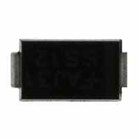
SURFACE MOUNT SCHOTTKY BARRIER RECTIFIER
Features
DO-214AC/SMA
The plastic package carries Underwriters Laboratory
Flammability Classification 94V-0
For surface mounted applications
Metal silicon junction,majority carrier conduction
Low power loss,high efficiency
Built-in strain relief,ideal for automated placement
0.110(2.80)
0.090(2.30)
0.067 (1.70)
0.051 (1.30)
High forward surge current capability
High temperature soldering guaranteed:
0.177(4.50)
0.150(3.80)
0.012(0.305)
0.006(0.152)
250 °C/10 seconds at terminals
0.097(2.45)
0.073(1.85)
Mechanical Data
0.061(1.55)
0.029(0.75)
Ca s e : JEDEC DO-214AC/SMA molded plastic body
Termina ls : Solderable per MIL-STD-750,Method 2026
Po larity : Color band denotes cathode end Moun ting
Po s ition : Any
Weigh t : 0.002 ounce, 0.07 grams
0.008(0.20)
0.002(0.05)
0.209(5.30)
0.184(4.70)
Dimensions in inches and (millimeters)
Maximum Ratings And Electrical Characteristics
Ratings at 25 C ambient temperature unless otherwise specified.
Single phase half-wave 60Hz,resistive or inductive load,for capacitive load current derate by 20%.
Parameter
SYMBOLS
MDD
SS12
MDD
SS13
MDD
SS14
MDD
SS15
MDD
SS16
MDD
SS18
MDD
SS110
MDD
SS1150
MDD
SS1200
UNITS
Maximum repetitive peak reverse voltage
VRRM
20
30
40
50
60
80
100
150
200
V
Maximum RMS voltage
Maximum DC blocking voltage
VRMS
VDC
14
20
21
30
28
40
35
50
42
60
56
80
70
100
105
150
140
200
V
V
Marking Code
I(AV)
1.0
A
8.3ms single half sine-wave
superimposed onrated load (JEDEC Method)
IFSM
25
A
Maximum instantaneous forward voltage at 1.0A
Maximum DC reverse current
TA=25℃
at rated DCblocking voltage
TA=100℃
VF
Maximum average forward rectified current
Peak forward surge current
Typical junction capacitance (NOTE 1)
Typical thermal resistance (NOTE 2)
Operating junction temperature range
Storage temperature range
0.55
0.3
10.0
IR
CJ
110
0.70
0.85
0.2
5.0
0.9
V
0.1
2.0
pF
80
RθJA
90.0
TJ
-55 to +150
℃
TSTG
-55 to +150
℃
℃/W
Note:1.Measured at 1MHz and applied reverse voltage of 4.0V D.C.
2.P.C.B. mounted with 2.0”x2.0”(5.0x5.0cm) copper pad areas
http://www.microdiode.com
mA
Rev:2025A5
Page :1
�SS12 THRU SS1200
Reverse Voltage - 20 to 200 Volts
Forward Current - 1.0 Ampere
Typical Characterisitics
Fig.1 Forward Current Derating Curve
Fig.2 Typical Reverse Characteristics
Instaneous Reverse Current ( μA)
Average Forward Current(A)
1.5
1.0
0.5
Single phase half-wave 60 Hz
resistive or inductive load
0.0
25
50
75
100
125
150
10
4
10
3
10
2
TJ=100°C
TJ=75°C
SS12~SS16
SS18~SS1200
101
10
TJ=25°C
0
0
Case Temperature(℃)
40
20
60
100
80
Percent of Rated Peak Reverse Voltage(%)
Fig.3 Typical Forward Characteristic
Fig.4 Typical Junction Capacitance
500
20
TJ=25°C
200
1.0
Junction Capacitance (pF)
Instaneous Forward Current (A)
10
SS12~SS14
SS15~SS16
SS18~SS110
SS1150~SS1200
0.1
0
0.2
0.4
0.6
0.8
1.0
1.2
1.4
1.6
100
50
SS12~SS14
20
SS15~SS1200
10
1.8
0.1
Fig.5 Maximum Non-Repetitive Peak
Forward Surage Current
100
25
20
15
10
05
8.3 ms Single Half Sine Wave (JEDEC
Method)
1
10
Number of Cycles at 60Hz
100
Transient Thermal Impedance(°C/W)
Peak Forward Surage Current (A)
100
Fig.6- Typical Transient Thermal Impedance
30
00
10
1
Reverse Voltage (V)
Instaneous Forward Voltage (V)
10
1
0.01
0.1
1
10
100
t, Pulse Duration(sec)
The curve above is for reference only.
http://www.microdiode.com
Rev:2025A5
Page :2
�SS12 THRU SS1200
Reverse Voltage - 20 to 200 Volts
Forward Current - 1.0 Ampere
Packing information
unit:mm
P0
P1
Item
D1
Symbol
Tolerance
SMA
A
B
C
d
D
D1
D
D1
D2
E
F
P
P0
P1
T
W
W1
0.1
0.1
0.1
0.05
2.0
min
2.0
min
0.5
0.1
0.1
0.1
0.1
0.1
0.1
0.3
1.0
2.80
5.33
2.36
1.50
330.00
50.00
178.00
62.00
13.00
1.75
5.50
4.00
4.00
2.00
0.28
12.00
18.00
d
E
W1
F
B
A
W
P
D2
T
C
D
Carrier width
Carrier length
Carrier depth
Sprocket hole
13" Reel outside diameter
13" Reel inner diameter
7" Reel outside diameter
7" Reel inner diameter
Feed hole diameter
Sprocket hole position
Punch hole position
Punch hole pitch
Sprocket hole pitch
Embossment center
Overall tape thickness
Tape width
Reel width
Note:Devices are packed in accor dance with EIA standar RS-481-A and specifications listed above.
Reel packing
PACKAGE
SMA
REEL SIZE
REEL
(pcs)
COMPONENT
SPACING
(m/m)
BOX
(pcs)
INNER BOX
(m/m)
REEL DIA,
(m/m)
CARTON SIZE
(m/m)
13"
5,000
4. 0
10,000
340*350*40
330
370*370*370
CARTON
(pcs)
80,000
Suggested Pad Layout
Symbol
A
Unit (mm)
1.68
Unit (inch)
0.066
B
1.52
0.060
C
3.93
0.154
D
2.41
0.095
E
5.45
0.215
Important Notice and Disclaimer
Microdiode Electronics (Shenzhen) reserves the right to make changes to this document and its products and specifications
at any time without notice. Customers should obtain and confirm the latest product information and specifications before final
design,purchase or use.
Microdiode Electronics (Shenzhen) makes no warranty, representation or guarantee regarding the suitability of its products
for any particular purpose, not does Microdiode Electronics (Shenzhen) assume any liability for application assistance or
customer product design. Microdiode Electronics (Shenzhen) does not warrant or accept any liability with products which are
purchased or used for any unintended or unauthorized application.
No license is granted by implication or otherwise under any intellectual property rights of Microdiode Electronics (Shenzhen).
Microdiode Electronics (Shenzhen) products are not authorized for use as critical components in life support devices or
systems without express written approval of Microdiode Electronics (Shenzhen).
http://www.microdiode.com
Rev:2025A2
Page :3
�
很抱歉,暂时无法提供与“SS12”相匹配的价格&库存,您可以联系我们找货
免费人工找货- 国内价格
- 1+0.23415
- 500+0.07791
- 2500+0.05198
- 5000+0.04263
- 国内价格
- 1000+0.07458
- 5000+0.05718
- 国内价格
- 10+0.06354
- 50+0.05862
- 200+0.05452
- 600+0.05043
- 1500+0.04715
- 3000+0.04510
- 国内价格
- 50+0.12420
- 500+0.10034
- 1500+0.08705
- 5000+0.07053
- 25000+0.06362
- 50000+0.05984