Sunlord
Specifications for Multi-layer Chip Power Inductor
Page 1 of 9
S P E C I F I C AT I O N S
Customer
Product Name
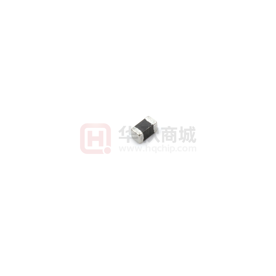
Multi-layer Chip Power Inductor
Sunlord Part Number
MPL1608S4R7MHT
Customer Part Number
[
New Released,
Revised]
SPEC No.: MPL081900030
Rev.
Effective Date
Changed Contents
Change Reasons
Approved By
01
Jun.11,2019
New release
/
Hai Guo
【This SPEC is total 9 pages including specifications and appendix.】
【ROHS Compliant Parts】
Approved By
Checked By
Issued By
Shenzhen Sunlord Electronics Co., Ltd.
Address: Sunlord Industrial Park, Dafu Industrial Zone, Baoan, Shenzhen, China
518110
Tel: 0086-755-29832660
Fax: 0086-755-82269029
E-Mail: sunlord@sunlordinc.com
【For Customer approval Only】
Qualification Status:
Full
Approved By
Comments:
Verified By
Date:
Restricted
Rejected
Re-checked By
Checked By
�Sunlord
Specifications for Multi-layer Chip Power Inductor
Page 2 of 9
Caution
All products listed in this specification are developed, designed and intended for use in general electronics equipment. The
products are not designed or warranted to meet the requirements of the applications listed below, whose performance and/or
quality require especially high reliability, or whose failure, malfunction or trouble might directly cause damage to society,
person, or property. Please understand that we are not responsible for any damage or liability caused by use of the products in
any of the applications below. Please contact us for more details if you intend to use our products in the following applications.
1. Aircraft equipment
2. Aerospace equipment
3. Undersea equipment
4. nuclear control equipment
5. military equipment
6. Power plant equipment
7. Medical equipment
8. Transportation equipment (automobiles, trains, ships,etc.
9. Traffic signal equipment
10. Disaster prevention / crime prevention equipment
11. Data-processing equipment
12. Applications of similar complexity or with reliability requirements comparable to the applications listed in the above
�Sunlord
1.
Specifications for Multi-layer Chip Power Inductor
Page 3 of 9
Scope
This specification applies to MPL1608S4R7MHT of multi-layer chip power inductors
2.
Product Description and Identification (Part Number)
1)
Description
MPL1608S4R7MHT of multi-layer chip power inductors.
2)
Product Identification (Part Number)
MPL
1608
S
4R7
M
H
T
②
③
④
⑤
⑥
⑦
①
②External Dimensions (L x W) (mm)
①Type
MPL
Chip Power Inductor
1608 [0603]
1.6 × 0.8
③Feature Type
S
Standard
④Nominal Inductance
Example
Nominal Value
4R7
4.7μH
⑤Inductance Tolerance
M
±20%
⑦Packing
⑥Thickness
H
3.
T
0.9 mm
Tape Carrier Package
Electrical Characteristics
Temperature
Part Number
MPL1608S4R7MHT
4.
L Test Freq.
S.R.F
DCR
Rise Current
Current
(μH)
(MHz)
Min. (MHz)
(Ω)
IDC1(mA.)
IDC2 (mA)
(max.)
(Typ.)
4.7
1
40
0.45±25%
620
100
1)
Operating and storage temperature range (individual chip without packing): -40℃ ~ +85℃
2)
Storage temperature range (packaging conditions): -10℃~+40℃ and RH 70% (Max.)
Shape and Dimensions
1)
Dimensions and recommended PCB pattern for reflow soldering: See Fig.4-1, Fig.4-2 and Table 4-1.
2)
Structure: See Fig. 4-3 and Fig. 4-4.
Solder-resist
Chip inductor
C
Land pattern
B
Fig. 4-1
Type
L
[Table 4-1]
W
A
B
Fig. 4-2
T
Unit: mm [inch]
a
1608
1.60±0.15
0.8±0.15
0.8±0.15
0.3±0.2
[0603]
[.063±.006]
[.031±.006]
[.031±.006]
[.012±.008]
T
Structure of
B
C
0.6~0.8
0.6~0.8
0.6~0.8
② Internal electrode (Ag)
T
a
Ferrite
Sn
④-2 Outside (Electro-plating Ni-Sn)
④-1
③
Fig. 4-3
③ Pull out electrode( Ag)
④-1 Terminal electrode: Inside (Ag)
Ni
W
④-2
②
A
① Ferrite for MPL Series
Electro-plating
L
a
①
Saturation
L
Ag
④
Fig. 4-4
�Sunlord
3)
Specifications for Multi-layer Chip Power Inductor
Page 4 of 9
Material Information: See Table 4-2.
[Table 4-2]
5.
Code
Part Name
Material Name
①
Ferrite Body
Ferrite Powder
②
Inner Coils
Silver Paste
③
Pull-out Electrode (Ag)
Silver Paste
④-1
Terminal Electrode: Inside Ag
Termination Silver Composition
④-2
Electro-Plating: Ni/Sn plating
Plating Chemicals
Test and Measurement Procedures
5.1 Test Conditions
Unless otherwise specified, the standard atmospheric conditions for measurement/test as:
a.
Ambient Temperature: 20±15℃
b.
Relative Humidity: 65±20%
c.
Air Pressure: 86 kPa to 106 kPa
If any doubt on the results, measurements/tests should be made within the following limits:
a.
Ambient Temperature: 20±2℃
b.
Relative Humidity: 65±5%
c.
Air Pressure: 86kPa to 106 kPa
5.2 Visual Examination
a.
Inspection Equipment: 20× magnifier
5.3 Electrical Test
5.3.1 DC Resistance (DCR)
a.
Refer to Item 3.
b.
Test equipment (Analyzer): High Accuracy Milliohmmeter-HP4338B or equivalent.
5.3.2 Inductance (L)
a.
Refer to Item 3.
b.
Test equipment: High Accuracy RF Impedance /Material Analyzer-HP4291B+HP16192A or equivalent.
c.
Test signal: -20dBm or 50mV.
d.
Test frequency refers to Item 3.
5.3.3 Temperature Rise Current(IDC1)
a.
Refer to Item 3.
b.
Test equipment (see Fig. 5.3.3-1): Electric Power, Electric current meter, Thermometer.
c.
Measurement method (see Fig. 5.3.3-1):
1. Set test current to be 0 mA.
2. Measure initial temperature of chip surface.
3. Gradually increase voltage and measure chip temperature for corresponding current.
4. Definition of Temperature Rise Current(IDC1): IDC1 is direct electric current as chip surface temperature rose just 40℃
against chip initial surface temperature (Ta) (see Fig. 5.3.3-2)
Thermometer
Electric Power
Temperature (℃)
Electric
Current Meter
Chip
+40
Ta
R
I (mA)
0
Fig. 5.3.3-1
IDC1
Fig. 5.3.3-2
�Sunlord
Specifications for Multi-layer Chip Power Inductor
Page 5 of 9
5.3.4 Saturation Current(IDC2)
a.
Refer to Item 3.
b.
Test equipment: HP6632B system DC power supply, HP4291B+HP16192A+HP16200A or equivalent.
c.
Measurement method:
1. Measurement conditions of initial inductance L: Measuring Frequency: 1MHz.
Test Current: 1mA.
2. Raising the voltage of the DC power supply, measure the inductance at the various current.
The rated current is the value of DC current at which the inductance will be 30% down compared with the initial
inductance value.
Note: In the period of raising voltage, voltage cannot be reduced.
3.
Definition of Saturation Current(IDC2): IDC2 is the value of DC current as inductance L (μH) decreased just 30% against
initial value (see Fig. 5.3.4-1).
+L0
70% L0
0
IDC2
I (mA)
Fig. 5.3.4-1
5.3.5Self-Resonant Frequency (SRF)
a.
Refer to Item 3.
b.
Test equipment: High Accuracy RF Impedance /Material Analyzer-HP4291B+HP16192A or equivalent.
c.
Test signal: -20dBm or 50 mV.
�Sunlord
Specifications for Multi-layer Chip Power Inductor
Page 6 of 9
5.4 Reliability Test
Items
Requirements
Test Methods and Remarks
5.4.1
No removal or split of the termination or other defects
Terminal
shall occur.
①
Solder the inductor to the testing jig (glass epoxy board
shown in Fig.5.4.1-1) using eutectic solder. Then apply a
Strength
10N force in the direction of the arrow.
Chip
F
Mounting Pad
②
Keep time: 10±1s.
③
Speed: 1.0mm/s.
①
Solder the inductor to the test jig (glass epoxy board shown
Glass Epoxy Board
Fig.5.4.1-1
5.4.2
No visible mechanical damage.
Resistance
in Fig.5.4.2-1) Using a eutectic solder. Then apply a force in
Unit: mm [inch]
to Flexure
the direction shown Fig. 5.4.2-2.
②
Flexure: 2mm.
Type
a
b
c
③
Pressurizing Speed: 0.5mm/sec.
1608[0603]
1.0
3.0
1.2
④
Keep time: 30 sec.
20
10
R230
Φ4.5
b
Flexure
40
c
a
45[1.772]
45[1.772]
100
Fig. 5.4.2-2
Fig.5.4.2-1
5.4.3
①
No visible mechanical damage.
Vibration
②
Inductance change: Within ±20%.
①
shown in Fig.5.4.3-1) using eutectic solder.
②
Cu pad
Solder the inductor to the testing jig (glass epoxy board
Solder mask
The inductor shall be subjected to a simple harmonic
motion having total amplitude of 1.5mm, the frequency
being varied uniformly between the approximate limits of 10
and 55 Hz.
③
The frequency range from 10 to 55 Hz and return to 10 Hz
shall be traversed in approximately 1 minute. This motion
shall be applied for a period of 2 hours in each 3mutually
Glass Epoxy Board
Fig. 5.4.3-1
perpendicular directions (total of 6 hours).
5.4.4
①
No visible mechanical damage.
Drop chip inductor 10 times on a concrete floor from a height of
Dropping
②
Inductance change: Within ±20%.
100 cm.
5.4.5
Inductance change should be within ±20% of initial value
Temperature range: -40℃~ +85℃
Temperature
measuring at 20℃.
Reference temperature: +20℃
5.4.6
①
No visible mechanical damage.
①
Solder temperature: 240±2℃
Solderability
②
Wetting shall exceed 95% coverage.
②
Duration: 3 sec.
③
Solder: Sn/3.0Ag/0.5Cu.
④
Flux: 25% Resin and 75% ethanol in weight.
5.4.7
①
No visible mechanical damage.
①
Solder temperature: 260±3℃.
Resistance to
②
Wetting shall exceed 95% coverage.
②
Duration: 5 sec.
Soldering Heat
③
Inductance change: Within ±20%.
③
Solder: Sn/3.0Ag/0.5Cu.
④
Flux: 25% Resin and 75% ethanol in weight.
⑤
The chip shall be stabilized at normal condition for 1~2
hours before measuring.
�Sunlord
Specifications for Multi-layer Chip Power Inductor
Items
Requirements
Test Methods and Remarks
5.4.8
①
No mechanical damage.
Thermal Shock
②
Inductance change: Within ±20%.
30 min.
85℃
Ambient
8
Temperature
5℃
Page 7 of 9
①
Temperature, Time: (See Fig.5.4.8-1)
②
Transforming interval: 20 sec.(max.).
③
Tested cycle: 100 cycles.
④
The chip shall be stabilized at normal condition for 1~2
-40℃ for 30±3 min→ 85℃ for 30±3min.
30 min.
hours before measuring.
-40℃
30 min.
20sec. (max.)
Fig. 5.4.8-1
5.4.9 Resistance
① No mechanical damage.
①
Temperature: -40±2℃
to Low
② Inductance change: Within ±20%.
②
Duration: 1000
③
The chip shall be stabilized at normal condition for 1~2
Temperature
+24
hours.
hours before measuring.
5.4.10
① No mechanical damage.
①
Temperature: 85±2℃
Resistance to
② Inductance change: Within ±20%.
②
Duration: 1000
③
The chip shall be stabilized at normal condition for 1~2
High
Temperature
+24
hours.
hours before measuring.
5.4.11
①
No visible mechanical damage.
①
Temperature: 60±2℃
Damp Heat
②
Inductance change: Within ±20%.
②
Humidity: 90% to 95% RH.
③
Duration: 1000
④
The chip shall be stabilized at normal condition for 1~2
(Steady States)
+24
hours.
hours before measuring.
6.
Packaging and Storage
6.1 Packaging
Tape Carrier Packaging:
Packaging code: T
(1)
a.
Tape carrier packaging are specified in attached figure Fig.6.1-1~3
b.
Tape carrier packaging quantity please see the following table:
Type
1608[0603]
T(mm)
0.8±0.15
Tape
PaperTape
Quantity
4K
c.
Reel shall be packaged in vinyl bag.
d.
Maximum of 5 or 10 reels bags shall be packaged in an inner box.
e.
Maximum of 6 or 10 inner boxes shall be packaged in an outer case.
Taping Drawings (Unit: mm)
Paper Tape
Top Tape
Paper Tape
Sprocket Hole
Bottom Tape
Chip Cavity
Fig 6.1-1
Remark: The sprocket holes are to the right as the tape is pulled toward the user.
�Sunlord
(2)
Specifications for Multi-layer Chip Power Inductor
Page 8 of 9
Taping Dimensions (Unit: mm)
+0.1
Sprocket Hole Φ1.5
-0
Chip Cavity
1.75±0.1
B
8.0±0.3
3.5±0.05
A
Type
A
B
P
Tmax
MPL1608_H
1.0±0.2
1.8±0.2
4.0±0.1
1.1
T
P
4.0±0.1
Direction of Feed
Fig 6.1-2
(3) Reel Dimensions (Unit: mm)
4.3±0.2mm
C
4.0±0.1mm
8.4+1.5/-0.0mm
2.45±0.2mm
5.0±0.1mm
58±2.0mm
13.5±0.2mm
3.0±0.1mm
max<14.4mm
178±2.0mm
Fig. 6.1-3
6.2 Storage
a.
The solderability of the external electrode may be deteriorated if packages are stored
9 where they are exposed to high humidity.
Package must be stored at 40℃ or less and 70% RH or less.
b.
9
The solderability of the external electrode may be deteriorated if packages are stored where they are exposed to dust of harmful gas
(e.g. HCl, sulfurous gas of H2S).
±
c.
Packaging material may be deformed if package are stored where they are exposed
0 to heat of direct sunlight.
d.
Solderability specified in Clause 5.4.6 shall be guaranteed for 12 months from the date of delivery on condition that they are stored at
.
the environment specified in Clause 3 .For those parts, which passed more than 12 months shall be checked solder-ability before use.
3
�Sunlord
7.
Specifications for Multi-layer Chip Power Inductor
Page 9 of 9
Recommended Soldering Technologies
7.1 Reflowing Profile:
△
Preheat condition: 150 ~200℃/60~120sec.
△
Allowed time above 217℃: 60~90sec.
△
Max temp: 260℃
△
Max time at max temp: 10sec.
△
Solder paste: Sn/3.0Ag/0.5Cu
△
Allowed Reflow time: 2x max
Peak 260℃ max
260℃
Max Ramp Up Rate=3℃/sec.
217℃
Max Ramp Down Rate=6℃/sec.
60~90sec.
200℃
150℃
60~120sec.
[Note: The reflow profile in the above table is only for
qualification and is not meant to specify board assembly
profiles. Actual board assembly profiles must be based on
25℃
Time 25℃ to Peak =8 min max
the customer's specific board design, solder paste and
process, and should not exceed the parameters as the
Reflow profile shows.]
7.2 Iron Soldering Profile.
3sec. Max.
△
Iron soldering power: Max.30W
△
Pre-heating: 150 ℃ / 60sec.
△
Soldering Tip temperature: 350℃Max.
Soldering Iron
△
Soldering time: 3sec Max.
Power: max. 30W
△
Solder paste: Sn/3.0Ag/0.5Cu
△
Max.1 times for iron soldering
350℃
Diameter of Soldering
[Note: Take care not to apply the tip of
the soldering iron to the terminal electrodes.]
8.
Iron 1.0mm max.
Tc ℃
Supplier Information
a) Supplier:
Shenzhen Sunlord Electronics Co., Ltd.
b)
Manufacturer:
Shenzhen Sunlord Electronics Co., Ltd.
c)
Manufacturing Address:
Sunlord Industrial Park, Dafuyuan Industrial Zone, Guanlan, Shenzhen, China
518110
�
很抱歉,暂时无法提供与“MPL1608S4R7MHT”相匹配的价格&库存,您可以联系我们找货
免费人工找货- 国内价格
- 20+0.15960
- 100+0.14535
- 500+0.13585
- 1000+0.12635
- 5000+0.11495
- 10000+0.11020
- 国内价格
- 20+0.33880
- 100+0.25330
- 1000+0.19650
- 4000+0.14230
- 20000+0.12820
- 国内价格
- 10+0.28383
- 100+0.23458
- 300+0.20996
- 1000+0.19149


 工商网监
湘ICP备2023018690号
工商网监
湘ICP备2023018690号
