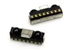
HSDL-3021
IrDA® Data Compliant Low Power 4.0 Mbit/s
with Remote Control Infrared Transceiver
Data Sheet
Description
Features
The HSDL-3021 is a new generation low profile
high speed enhanced infrared (IR) transceiver module that provides the capability of (1) interface between logic and IR signals for through-air, serial, half-
duplex IR data link, and (2) IR remote control transmission for universal remote control applications. The HSDL3021 can be used for IrDA as well as remote control application without the need of any additional external
components for multiplexing.
General Features
The HSDL-3021 is fully compliant to IrDA® Physical Layer
specification version 1.4 low power from 9.6 kbit/s to
4.0 Mbit/s (FIR) and IEC825 Class 1 eye safety standards.
The HSDL-3021 can be shut down completely to achieve
very low power consumption. In the shut-down mode,
the PIN diode will be inactive and thus produce very little
photocurrent even under very bright ambient light. It is
also designed to interface to input/output logic circuits
as low as 1.5 V. These features are ideal for battery operated mobile devices such as PDAs and mobile phones
that require low power consumption.
• Operating temperature from -25°C ~ 85°C
– Critical parameters are guaranteed over
temperature and supply voltage
• VCC supply 2.4 to 3.6 volts
• Miniature package
– Height: 2.5 mm
– Width: 8.0 mm
– Depth: 3.0 mm
• Integrated remote control LED driver
• Input/output interface voltage of 1.5 V
• Integrated EMI shield
• LED stuck-high protection
• Designed to accommodate light loss with cosmetic
windows
• IEC 825-Class 1 eye safe
• Interface to various super I/O and controller devices
• Lead free package
IrDA® Features
Applications
• Mobile data communication and universal remote
control
– Mobile phones
– PDAs
– Webpads
• Fully compliant to IrDA 1.4 Physical Layer Low Power
Specifications from 9.6 kbit/s to 4.0 Mb/s
– Link distance up to 50 cm typically
• Complete shutdown for TxD_IrDA, RxD_IrDA and PIN
diode
• Low power consumption
– Low shutdown current
Remote Control Features
• Wide angle and high radiant intensity
• Spectrally suited to remote control function at
890 nm typically
• Typical link distance up to 8 meters (on-axis)
�R2
LEDA
1
IOVCC
IOVCC
2
VLED
CX3
CX4
LED
DRIVER
CX5
3
RxD
4
SD
5
Rx PULSE
SHAPER
R1
VCC
SHIELD
TxD_IR
CX1
CX2
VCC
6
TxD_RC
7
GND
8
Figure 1. HSDL-3021 block diagram.
8
7
6
5
4
3
2
1
Figure 2. Pinout.
Application Support Information
The Application Engineering Group
is available to assist you with the
application design associated with
HSDL-3021 infrared transceiver
module. You can contact them
through your local sales representatives for additional details.
�
Order Information
Part Number
Packaging Type
Package
Quantity
HSDL-3021-021
Tape and Reel
Front Option
2500
Marking Information
The unit is marked with “HYWLL” on the shield
Y = Year
W = Work week
LL = Lot information
�I/O Pins Configuration Table
Pin
Symbol
Description
I/O Type
1
LEDA
LED Anode
Note 1
2
IOVCC
Input/Output ASIC Voltage
Note 2
3
TxD_IR
IrDA Transmitter Data Input
Input. Active High
Note 3
4
RxD
IrDA Receive Data
Output. Active Low
Note 4
5
SD
Shutdown
Input. Active High
Note 5
6
VCC
Supply Voltage
Note 6
7
TxD_RC
RC Transmitter Data Input
Note 7
8
GND
Ground
Note 8
–
Shield
EMI shield
Note 9
Input. Active High
Notes
Notes:
1. Tied through external resistor, R2, to Vled. Refer to the table below for recommended series resistor value.
2. Connect to ASIC logic controller supply voltage or VCC. The voltage at this pin should be equal to or less than VCC.
3. This pin is used to transmit serial data when SD pin is low. If held high for longer than 50 µs, the LED is turned off. Do NOT float this pin.
4. This pin is capable of driving a standard CMOS or TTL load. No external pull-up or pull-down resistor is required. The pin is in tri-state when the
transceiver is in shutdown mode.
5. Complete shutdown of IC and PIN diode. The pin is used for setting IR receiver bandwidth, range of IR LED current and RC drive programming
mode. Refer to section on “Bandwidth Selection Timing” and “Remote Control Drive Modes” for more information. Do NOT float this pin. ***
6. Regulated, 2.4 V to 3.6 V.
7. Logic high turns on the RC LED. If held high longer than 50 µs, the RC LED is turned off. Do NOT float the pin.
8. Connect to system ground.
9. Connect to system ground via a low inductance trace. For best performance, do not connect directly to the transceiver GND pin.
Recommended Application Circuit Components
Component
Recommended Value
Note
R1
4.7 Ω, ± 5%, 0.25 watt
R2
2.7 Ω, for 2.4 < VLED ≤ 2.7 V;
3.3 Ω, for 2.7 < VLED ≤ 3.0 V
3.9 Ω, for 3.0 < VLED ≤ 3.3 V
4.7 Ω, for 3.3 < VLED ≤ 3.6 V
5.6 Ω, for 3.6 < VLED ≤ 4.2 V
10 Ω, for 4.2 < VLED ≤ 5 V
CX1, CX3, CX5
100 nF, ± 20%, X7R Ceramic
1
CX2, CX4
4.7 µF, ± 20%, Tantalum
1
Note:
1. CX1, CX2, CX3 & CX4 must be placed within 0.7 cm of HSDL-3021 to obtain optimum noise
immunity.
CAUTIONS: The BiCMOS inherent to the design of this component increases the component’s susceptibility to damage
from electrostatic discharge (ESD). It is advised that normal static precautions be taken in handling and assembly of
this component to prevent damage and/or degradation which may be induced by ESD.
�
�Absolute Maximum Ratings
For implementations where case to ambient thermal resistance is ≤ 50°C/W.
Parameter
Symbol
Min.
Max.
Units
Storage Temperature
TS
-40
+100
°C
Operating Temperature
TA
-25
+85
°C
LED Anode Voltage
VLEDA
0
6.5
V
Supply Voltage
VCC
0
6
V
Input Voltage: TXD, SD/Mode
VI
0
5.5
V
Input/Output Supply Voltage: RXD
IOVCC
0
6
V
Conditions
IR LED Current Pulse Amplitude
I(VLED)IR
190
mA
≤ 25% duty cycle,
≤ 90 µs pulse width
RC LED Current Pulse Amplitude
I(VLED)RC
400
mA
≤ 10% duty cycle,
≤ 90 µs pulse width
Recommended Operating Conditions
Parameter
Symbol
Min.
Operating Temperature
TA
-25 +85
°C
Supply Voltage
VCC
2.4
3.6
V
Input/Output Voltage
IOVCC
1.5
3.6
V
Logic Input Voltage
for TXD, SD/Mode
VIH
VIL
IOVCC - 0.5
0
IOVCC
0.5
V
V
Logic High
Logic Low
Typ.
Max.
Units
0.0090
500
Receiver Input
Logic High
EIH
mW/cm2
Irradiance
0.0225
500
Logic Low
EIL
0.3
µW/cm2
IR LED (Logic High) Current Pulse
Amplitude – SIR Mode
ILEDA
65
mA
IR LED (Logic High) Current Pulse
Amplitude – MIR/FIR Mode
ILEDA
150
mA
RC LED (Logic High) Current Pulse
Amplitude
ILEDA
250
mA
Receiver Data Rate
0.0096
4.0
Ambient Light
Conditions
For in-band signals
≤ 115.2 kbit/s[3]
0.576 Mbit/s ≤ in-band
signals ≤ 4.0 Mbit/s[3]
For in-band signals[3]
Mbit/s
See IrDA Serial Infrared Physical Layer
Link Specification, Appendix A for
ambient levels
Note:
3. An in-band optical signal is a pulse/sequence where the peak wavelength, lp, is defined as 850 ≤ lp ≤ 900 nm, and the pulse characteristics
are compliant with the IrDA Serial Infrared Physical Layer Link Specification v1.4.
�
�Electrical and Optical Specifications
Specifications (Min. & Max. values) hold over the recommended operating conditions unless otherwise noted. Unspecified test conditions may be anywhere in their operating range. All typical values (Typ.) are at 25°C with VCC set
to 3.0 V and IOVCC set to 1.8 V unless otherwise noted.
Parameter
Symbol
Min.
Typ.
Max.
2q1/2
30
Units
Conditions
Receiver
Viewing Angle
Peak Sensitivity Wavelength lP
885
°
nm
RxD_IrDA Output
Logic High
VOH
IOVCC -0.5
IOVCC V
Voltage
Logic Low
IOH = -200 µA, EI ≤ 0.3
µW/cm2
VOL
0
0.4
V
RxD_IrDA Pulse Width (SIR)[4]
tRPW(SIR)
1
4
µs
q1/2 ≤ 15°, CL = 9 pF
RxD_IrDA Pulse Width (MIR)[4]
tRPW(MIR)
100
500
ns
q1/2 ≤ 15°, CL = 9 pF
RxD_IrDA Pulse Width (Single) (FIR)[4]
tRPW(FIR)
80
175
ns
q1/2 ≤ 15°, CL = 9 pF
RxD_IrDA Pulse Width (Double) (FIR)[4]
tRPW(FIR)
200
290
ns
q1/2 ≤ 15°, CL = 9 pF
40
ns
CL = 9 pF
RxD_IrDA Rise & Fall Times tr, tf
Receiver Latency Time[5]
tL
100
µs
EI = 9.0 µW/cm2
Receiver Wake Up Time[6]
tRW
200
µs
EI = 10 mW/cm2
Infrared (IR) Transmitter
IR Radiant Intensity (SIR Mode)
IEH
4
mW/sr
IR_ILEDA = 65 mA,
q1/2 ≤ 15°, TxD_IR ≥ VIH,
TA = 25°C
IR Radiant Intensity (MIR/FIR Mode)
IEH
10
mW/sr
IR_ILEDA = 150 mA,
q1/2 ≤ 15°, TxD_IR ≥ VIH,
TA = 25°C
IR Viewing Angle
2q1/2
30
60
IR Peak Wavelength
lP
TxD_IrDA Logic Levels
High
VIH
IOVCC - 0.5
IOVCC
V
Low
VIL
0
0.5
V
TxD_IrDA Input Current
High
IH
0.02
µA
VI ≥ VIH
Low
0 ≤ VI ≤ VIL
885
°
nm
IL
-0.02
µA
Wake Up Time[7]
tTW
180
ns
Maximum Optical Pulse Width[8]
tPW(max)
25
µs
50
TXD Pulse Width (SIR)
tPW(SIR)
1.6
µs
tPW (TXD_IR) = 1.6 µs at
115.2 kbit/s
TXD Pulse Width (MIR)
tPW(MIR)
217
ns
tPW (TXD_IR) = 217 ns at
1.152 Mbit/s
TXD Pulse Width (FIR)
tPW(FIR)
125
ns
tPW (TXD_IR) = 125 ns at
4.0 Mbit/s
TxD Rise & Fall Times (Optical)
tr, tf
600
ns
tPW (TXD_IR) = 1.6 µs at
115.2 kbit/s
40
ns
tPW (TXD_IR) = 125 ns at
4.0 Mbit/s
�
�Electrical and Optical Specifications (Cont’d.)
Parameter
Symbol
Min.
Typ.
Max.
Units
Conditions
IR LED Anode On-State Voltage
VON
2.19
V
(SIR Mode)
(IR_LEDA)
IR_ILEDA = 65 mA,
IR VLED = 3.6 V, R = 13 Ω,
VI (TxD) ≥ VIH
IR LED Anode On-State Voltage
VON
2.22
V
(MIR/FIR Mode)
(IR_LEDA)
IR_ILEDA = 150 mA,
IR VLED = 3.6 V, R = 13 Ω,
VI(TxD_IR) ≥ VIH
Remote Control (RC) Transmitter
RC Radiant Intensity
IEH
50
mW/sr
30
60
RC_ILEDA = 250 mA,
q1/2 ≤ 15°, TxD_RC ≥ VIH,
TA = 25°C
RC Viewing Angle
2q1/2
RC Peak Wavelength
lP
TxD_RC Logic Levels
High
VIH
IOVCC - 0.5
IOVCC
V
Low
VIL
0
0.5
V
TxD_RC Input Current
High
IH
0.02
1
µA
VI ≥ VIH
Low
IL
-0.02
1
µA
0 ≤ VI ≤ VIL
885
°
nm
RC LED Anode On-State Voltage
VON
2.08
V
(RC_LEDA)
RC_ILEDA = 250 mA,
RC VLED = 3.6 V, R = 3.9 Ω,
VI(TxD_RC) ≥ VIH
Transceiver
Input Current
High
IH
0.01
1
µA
VI ≥ VIH
Low
IL
-0.02
1
µA
0 ≤ VI ≤ VIL
Supply Current
Shutdown ICC1
1
µA
VSD ≥ VCC - 0.5, TA = 25°C
Idle
(Standby)
ICC2
2.0
2.9
mA
VI(TxD) ≤ VIL, EI = 0
Active
ICC3
3.5
mA
VI(TxD) ≥ VIL, EI = 10 mW/cm2
-1
Notes:
4. An in-band optical signal is a pulse/sequence where the peak wavelength, lP, is defined as 850 nm ≤ lP ≤ 900 nm, and the pulse characteristics are compliant with the IrDA Serial Infrared Physical Layer Link Specification version 1.4.
5. For in-band signals 115.2 kbit/s where 9 µW/cm2 ≤ EI ≤ 500 mW/cm2.
6. For in-band signals 1.152 Mbit/s where 22 µW/cm2 ≤ EI ≤ 500 mW/cm2.
7. For in-band signals 4 Mbit/s where 22 µW/cm2 ≤ EI ≤ 500 mW/cm2.
8. Latency is defined as the time from the last TxD_IrDA light output pulse until the receiver has recovered full sensitivity.
9. Receiver Wake Up Time is measured from VCC power ON to valid RxD_IrDA output.
10, Transmitter Wake Up Time is measured from VCC power ON to valid light output in response to a TxD_IrDA pulse.
11. The Max Optical PW is defined as the maximum time which the IR LED will turn on. This is to prevent the long Turn On time for the IR LED.
�
�Timing Waveforms
tpw
VOH
90%
50%
VOL
10%
tf
tr
Waveform 1. RXD output waveform
tpw
LED ON
90%
50%
LED OFF
10%
tr
tf
Waveform 2. LED optical waveform
TXD
LED
tpw (MAX.)
Waveform 3. TXD ”stuck on“ protection waveform
SD
SD
RX
LIGHT
TXD
RXD
TX
LIGHT
tRW
Waveform 4. Receiver wakeup time waveform
�
tTW
Waveform 5. TXD wakeup time waveform
�IR MIR/FIR Mode - VLED_A vs ILED
2.5
2.3
2.4
2.2
2.3
2.2
2.1
VLED_A (V)
VLED_A (V)
IR SIR Mode - VLED_A vs ILED
2.4
2.0
1.9
1.8
2.1
2.0
1.9
1.8
1.7
1.7
1.6
1.6
1.5
000.0E+0
1.5
20.0E-3
40.0E-3
60.0E-3
80.0E-3
0
100.0E-3
0.05
0.1
ILED (A)
IR SIR Mode - Radiant Intensity vs ILED
RADIANT INTENSITY (mW/sr)
RADIANT INTENSITY (mW/sr)
0.25
70
20
15
10
5
20.0E-3
40.0E-3
60.0E-3
ILED (A)
�
0.2
IR MIR/FIR Mode - Radiant Intensity vs ILED
25
0
000.0E+0
0.15
ILED (A)
80.0E-3
100.0E-3
60
50
40
30
20
10
0
0
0.05
0.1
0.15
ILED (A)
0.2
0.25
�HSDL-3021 Package Dimensions
MOUNTING
CENTER
4.0
1.025
2.05
CL
RC EMITTER AND
IrDA EMITTER
RECEIVER
2.5
1.175
0.35
0.65
0.80
2.55
2.85
4.0
8.0
3.0
2.9
1.85
CL
8
0.6
7
6
5
4
3
3.325
P 0.95 X 7 = 6.65
�
2
1
PIN 1
PIN 2
VLED
IOVCC
PIN 3
PIN 4
TxDR
RxD
PIN 5
PIN 6
PIN 7
PIN 8
SD
VDD
TxD RC
GND
UNIT: mm
PRODUCTION TOLERANCE: ± 0.2mm
�HSDL-3021 Tape and Reel Dimensions
4.0 ± 0.1
UNIT: mm
1.75 ± 0.1
+ 0.1
1.5 0
1.5 ± 0.1
POLARITY
PIN 8: VLED
7.5 ± 0.1
8.4 ± 0.1
16.0 ± 0.2
PIN 1: GND
0.4 ± 0.05
3.4 ± 0.1
8.0 ± 0.1
2.8 ± 0.1
EMPTY
PROGRESSIVE DIRECTION
PARTS MOUNTED
LEADER
(400 mm MIN.)
(40 mm MIN.)
EMPTY
(40 mm MIN.)
OPTION #
"B"
"C"
QUANTITY
001
178
60
500
021
330
80
2500
UNIT: mm
DETAIL A
2.0 ± 0.5
B
C
13.0 ± 0.5
R 1.0
LABEL
21 ± 0.8
DETAIL A
16.4 +02
2.0 ± 0.5
10
�HSDL-3021 Moisture Proof Packaging
Recommended Storage Conditions
All HSDL-3021 options are shipped in moisture proof
package. Once opened, moisture absorption begins.
Storage Temperature 10°C to 30°C
This part is compliant to JEDEC Level 4.
Time From Unsealing To Soldering
Relative Humidity
Below 60% RH
After removal from the bag, the parts should be soldered
within three days if stored at the recom-mended storage
conditions. When MBB (Moisture Barrier Bag) is opened
and the parts are exposed to the recommended storage
conditions more than three days but less than 15 days,
the parts must be baked before reflow to prevent damage to the parts.
UNITS IN A SEALED
MOISTURE-PROOF
PACKAGE
PACKAGE IS OPENED
(UNSEALED)
Note: Using the parts that are exposed for more than 15 days is not
recommended.
Baking Conditions
Package
ENVIRONMENT
LESS THAN 30¡C,
AND LESS THAN
60% RH
Temp
In reels 60°C
YES
Time
≥ 48 hours
In bulk
100°C ≥ 4 hours
125°C ≥ 2 hours
Note: Baking should only be done once.
NO BAKING
IS NECESSARY
PACKAGE IS
OPENED LESS
THAN 72 HOURS
YES
NO
PERFORM RECOMMENDED
BAKING CONDITIONS
Figure 3. Baking conditions chart.
11
NO
�Recommended Reflow Profile
MAX. 260°C
T – TEMPERATURE – (°C)
255
R3
230
217
200
R2
180
60 sec.to 90 sec.
ABOVE
217°C
150
R1
120
R4
R5
80
25
50
0
P1
HEAT
UP
100
150
200
250
t-TIME (SECONDS)
P2
P3
SOLDER PASTE DRY
SOLDER
REFLOW
300
P4
COOL
DOWN
Process Zone
Symbol
DT
Maximum DT/DTime or Duration
Heat Up
P1, R1
25°C to 150°C
3°C/s
Solder Paste Dry
P2, R2
150°C to 200°C
100s to 180s
Solder Reflow
P3, R3
P3, R4
200°C to 260°C
260°C to 200°C
3°C/s
-6°C/s
Cool Down
P4, R5
200°C to 25°C
-6°C/s
Time maintained above
liquidus point, 217°C
>217°C
60s to 90s
Peak Temperature
260°C
–
Time within 5°C of actual
Peak Temperature
–
20s to 40s
Time 25°C to Peak Temperature
25°C to 260°C
8 mins
The reflow profile is a straight-line representation of a
nominal temperature profile for a convective reflow solder process. The temperature profile is divided into four
process zones, each with different DT/Dtime temperature change rates, or duration. The DT/Dtime rates, or duration, are detailed in the above table. The temperatures
are measured at the component to printed circuit board
connections.
In process zone P1, the PC board and HSDL-3021 pins are
heated to a temperature of 150°C to activate the flux in
the solder paste. The temperature ramp up rate, R1, is
limited to 3°C per second to allow for even heating of
both the PC board and HSDL-3021 pins.
Process zone P2 should be of sufficient time duration (100
to 180 seconds) to dry the solder paste. The temperature
is raised to a level just below the liquidus point of the
solder.
Process zone P3 is the solder reflow zone. In zone P3, the
temperature is quickly raised above the liquidus point
of solder to 260°C (500°F) for optimum results. The dwell
time above the liquidus point of solder should be between 60 and 90 seconds. This is to assure proper coalescing of the solder paste into liquid solder and the
formation of good solder connections. Beyond the recommended dwell time, the intermetallic growth within
the solder connections becomes excessive, resulting in
the formation of weak and unreliable connections. The
temperature is then rapidly reduced to a point below
the solidus temperature of the solder to allow the solder
within the connections to freeze solid.
Process zone P4 is the cool down after solder freeze. The
cool down rate, R5, from the liquidus point of the solder
to 25°C (77°F) should not exceed 6°C per second maximum. This limitation is necessary to allow the PC board
and HSDL-3021 pins to change dimensions evenly, putting minimal stresses on the HSDL-3021.
It is recommended to perform reflow soldering no more
than twice.
12
�Appendix A: HSDL-3021 SMT Assembly Application Note
Solder Pad, Mask and Metal Stencil
METAL STENCIL
FOR SOLDER PASTE
PRINTING
STENCIL
APERTURE
LAND
PATTERN
SOLDER
MASK
PCBA
Figure 1. Stencil and PCBA.
Recommended Land Pattern
MOUNTING CENTER
2.7
MOUNTING CENTER
1.25
2.05
0.10
0.775
1.75
FIDUCIAL
0.475
0.6
0.35
1.425
2.375
Figure 2.
13
�Recommended Metal solder Stencil Aperture
APERTURES AS PER
LAND DIMENSIONS
It is recommended that only a 0.152 mm (0.006 inch) or
a 0.127 mm (0.005 inch) thick stencil be used for solder
paste printing. This is to ensure adequate printed solder
paste volume and no shorting. See Table 1 below the
drawing for combinations of metal stencil aperture and
metal stencil thickness that should be used. Aperture
opening for shield pad is 3.05 mm x 1.1 mm as per land
pattern.
t
w
l
Figure 3. Solder stencil aperture.
Table 1.
Stencil Thickness,
t (mm)
0.127 mm
0.11 mm
Adjacent Land Keepout and Solder Mask Areas
Adjacent land keepout is the maximum space occupied
by the unit relative to the land pattern. There should be
no other SMD components within this area. The minimum solder resist strip width required to avoid solder
bridging adjacent pads is 0.2 mm. It is recommended
that two fiducial crosses be placed at mid length of the
pads for unit alignment.
Note: Wet/Liquid Photo-imaginable solder resist/mask is recommended.
j
k
h
l
SOLDER MASK
14
DIMENSION
mm
h
0.2
l
3.0
k
3.85
j
10.1
Aperture Size(mm)
Length, l
1.75 ± 0.05
2.4 ± 0.05
Width, w
0.55 ± 0.05
0.55 ± 0.05
�Appendix B: PCB Layout Suggestion
The effects of EMI and power supply noise can potentially reduce the sensitivity of the receiver, resulting in reduced link distance. The PCB layout played an important
role to obtain a good PSRR and EM immunity resulting in
good electrical performance. Things to note:
1. The ground plane should be continuous under the
part, but should not extend under the shield trace.
2. The shield trace is a wide, low inductance trace back
to the system ground. CX1, CX2, CX3, CX4 and CX5 are
optional supply filter capacitors; they may be left out
if a clean power supply is used.
3. VLED can be connected to either unfiltered or
unregulated power supply. The bypass capacitors
should be connection before the current limiting
resistor R2 respectively. In a noisy environment,
including capacitor CX3and CX4 can enhance supply
rejection. CX3 that is generally a ceramic capacitor of
low inductance providing a wide frequency response
while CX4 is tantalum capacitor of big volume and fast
frequency response. The use of a tantalum capacitor
is more critical on the VLED line, which carries a high
current.
4. VCC pin can be connected to either unfiltered or
unregulated power supply. The Resistor, R1 together
with the capacitors, CX1 and CX2 acts as the low pass
filter.
5. IOVCC is connected to the ASIC voltage supply or the
VCC supply. The capacitor, CX5 acts as the bypass
capacitor.
6. Preferably a multi-layered board should be used
to provide sufficient ground plane. Use the layer
underneath and near the transceiver module as Vcc,
and sandwich that layer between ground connected
board layers. The diagram below demonstrate an
example of a 4 layer board:
15
• Top Layer: Connect the metal shield and module
ground pin to bottom ground layer; Place the bypass
capacitors within 0.5 cm from the VCC and ground pin
of the module.
• Layer 2: Critical ground plane zone. 3 cm in all directions
around the module. Connect to a clean, noiseless
ground node (e.g., bottom layer).
• Layer 3: Keep data bus away from critical ground plane
zone.
• Bottom layer: Ground layer. Ground noise


 工商网监
湘ICP备2023018690号
工商网监
湘ICP备2023018690号
