UC2842/44/45
UC3842/43/45
CURRENT MODE PWM CONTROLLER
DESCRIPTION
The UC284x and UC384x are fixed frequency current mode PWM controller.
They are specially designed for OFF Line and DC to DC converter
applications with a minimal external components. Internally implemented
circuits include a trimmed oscillator for precise duty cycle control, a
temperature compensated reference, high gain error amplifier, current
sensing comparator, and a high current totem pole output ideally suited for
driving a power MOSFET. Protection circuitry includes built under voltage
lockout and current limiting.
The UC2842/44, UC3842/44 have UVLO thresholds of 16 V (on) and 10 V (off).
The corresponding thresholds for the UC2843/45, UC3843/45 are 8.4V (on)
and 7.6V (off).
The UC2842/43, UC3842/43 can operate within 100% duty cycle.
The UC2844/45, UC3844/45 can operate within 50% duty cycle.
The UC2842/44/44/45 is characterized for operation from TA = -40℃ to 85℃.
The UC3842/43/44/45 is characterized for operation from TA = 0℃ to 70℃.
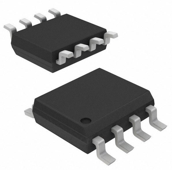
DIP8
SOP8
FEATURES
Low Start-Up and Operating Current
Under voltage Lockout With Hysteresis
High Current Totem Pole Output
Operating Frequency Up To 500KHz
ORDERING INFORMATION
DEVICE
Package Type
MARKING
Packing
Packing Qty
UC2842N
DIP8
UC2842
TUBE
2000/box
UC2843N
DIP8
UC2843
TUBE
2000/box
UC2844N
DIP8
UC2844
TUBE
2000/box
UC2845N
DIP8
UC2845
TUBE
2000/box
UC2842M/TR
SOP8
UC2842
REEL
2500/reel
UC2843M/TR
SOP8
UC2843
REEL
2500/reel
UC2844M/TR
SOP8
UC2844
REEL
2500/reel
UC2845M/TR
SOP8
UC2845
REEL
2500/reel
UC3842N
DIP8
UC3842
TUBE
2000/box
UC3843N
DIP8
UC3843
TUBE
2000/box
UC3844N
DIP8
UC3844
TUBE
2000/box
UC3845N
DIP8
UC3845
TUBE
2000/box
UC3842M/TR
SOP8
UC3842
REEL
2500/reel
UC3843M/TR
SOP8
UC3843
REEL
2500/reel
UC3844M/TR
SOP8
UC3844
REEL
2500/reel
UC3845M/TR
SOP8
UC3845
REEL
2500/reel
http://www.hgsemi.com.cn
1 / 11
2020 SEP
�UC2842/44/45
UC3842/43/45
Pin CONNECTION
DIP8/SOP8
PIN FUNCTION
N
FUNCTION
1
COMP
2
VFB
3
ISENSE
A voltage proportional to inductor current is connected to this input. The PWM uses this information
to terminate the output switch conduction.
4
RT/CT
The oscillator frequency and maximum Output duty cycle are programmed by connecting resistor
RT to Vref and capacitor CT to ground.
5
GROUND
6
OUTPUT
7
8
VCC
Vref
DESCRIPTION
This pin is the Error Amplifier output and is made for loop compensation.
This is the inverting input of the Error Amplifier. It is normally connected to the switching power
supply output through a resistor divider.
This pin is the combined control circuitry and power ground.
This output directly drives the gate of a power MOSFET. Peak currents up to 1A are sourced and
sink by this pin.
This pin is the positive supply of the integrated circuit.
This is the reference output. It provides charging current for capacitor CT through resistor RT .
BLOCK DIAGRAM
(toggle flip flop used only in UC2844/45, UC3844/45)
Absolute Maximum Ratings
Characteristic
Symbol
VCC
Supply Voltage (low impedance source)
Output Current
Input Voltage (Analog Inputs pins 2,3)
Error Amp Output Sink Current
Power Dissipation (TA=250C)
Storage Temperature Range
Lead Temperature (soldering 5 sec.)
http://www.hgsemi.com.cn
IO
VI
ISINK (E.A)
PO
Tstg
TL
2 / 11
Value
30
1
0.3 to 5.5
10
1
-65 to150
260
Unit
V
A
V
mA
W
℃
℃
2020 SEP
�UC2842/44/45
UC3842/43/45
Electrical characteristics (*VCC=15V, RT=10k , CT=3.3nF, TA=00C to +700C, unless otherwise specified)
Characteristics
Reference Section
Reference Output Voltage
Line Regulation
Load Regulation
Short Circuit Output Current
Oscillator Section
Oscillation Frequency
Symbol
VREF
VREF
VREF
Test Condition
TJ = 25°C, IREF = 1 mA
12V VCC 25 V
ISC
1 mA IREF 20mA
TA = 25°C
f
TJ = 25°C
Min
Typ
Max
Unit
4.9
5.0
6.0
5.1
20
V
6.0
-100
25
-180
mA
52
57
KHz
Frequency Change with Voltage f/VCC
V(OSC)
Oscillator Amplitude
12V VCC 25 V
(peak to peak)
0.05
1.6
1.0
%
V
Error Amplifier Section
Input Bias Current
VFB=3V
-0.1
-2
µA
2.58
V
dB
Input Voltage
Open Loop Voltage Gain
Unity Gain Bandwidth
Power Supply Rejection Ratio
Output Sink Current
Output Source Current
High Output Voltage
Low Output Voltage
Current Sense Section
Gain
Maximum Input Signal
Supply Voltage Rejection
Input Bias Current
Output Section
IBIAS
VI(E.A)
AVOL
UGBW
PSRR
ISINK
ISOURCE
VOH
VOL
GV
VI(MAX)
SVR
IBIAS
47
mV
Vpin1 = 2.5V
2V V0 4V
2.42
65
2.5
90
Tj=250C, Note 3
12V VCC 25 V
0.5
60
0.6
70
MHz
dB
Vpin2 = 2.7V, Vpin1 = 1.1V
Vpin2 = 2.3V, Vpin1 = 5V
2
-0.5
7
-1.0
mA
mA
Vpin2 = 2.3V, RL = 15K to GND
Vpin2 = 2.7V, RL = 15K to PIN 8
5.0
6.0
0.8
1.1
(Note 1 & 2)
2.85
3.0
3.15
V/V
V pin1 = 5V (Note1)
12V VCC 25 V (Note 1)
0.9
1.0
70
1.1
V
dB
Vpin3 = 3V
-3.0
-10
µA
0.08
1.4
0.4
2.2
Low Output Voltage
VOL
ISINK = 20 mA
ISINK = 200 mA
High Output Voltage
VOH
ISINK = 20 mA
ISINK = 200 mA
Rise Time
Fall Time
tR
tF
TJ = 25℃, CL = 1nF (Note 3)
TJ = 25℃, CL = 1nF (Note 3)
13
12
13.5
13.0
45
35
150
150
V
V
nS
Undervoltage Lockout Section
Start Theshold
VTH(ST)
Min. Operating Voltage
(After Turn On)
VOPR(min)
UC2842/44,UC3842/44
14.5
16.0
17.5
UC2843/45,UC3843/45
UC2842/44,UC3842/44
7.8
8.5
8.4
10
9.0
11.5
UC2843/45,UC3843/45
7.0
7.6
8.2
UC2842/43,UC3842/43
UC2844/45,UC3844/45
95
47
97
48
100
50
V
V
PWM Section
Max. Duty Cycle
D(MAX)
Min. Duty Cycle
Total Standby Current
D(MAX)
Start Up Current
Operating Supply Current
IST
ICC (OPR)
UC3842/43/44/45
Vpin3 = Vpin2 = 0V
Zener Voltage
VZ
ICC=25 mA
%
0
0.17
13
30
38
0.3
17
mA
V
* Adjust VCC above the start threshold before setting it to 15V.
Note 1: Parameter measured at trip point of latch with Vpin2=0.
Note 2: Gain defined as A=∆Vpin1/∆Vpin3 ; 0 ≤ Vpin3 ≤ 0.8V.
Note 3: These parameters, although guaranteed, are not 100% tested in production.
http://www.hgsemi.com.cn
3 / 11
2020 SEP
�UC2842/44/45
UC3842/43/45
APPLICATION INFORMATION
Figure 1. Error Amp Configuration
Figure 2. Under voltage Lockout
http://www.hgsemi.com.cn
4 / 11
2020 SEP
�UC2842/44/45
UC3842/43/45
Figure 3. Current Sense Circuit
Figure 4. Slope Compensation Techniques
http://www.hgsemi.com.cn
5 / 11
2020 SEP
�UC2842/44/45
UC3842/43/45
Figure 5. Latched Shutdown
Figure 6. Error Amplifier Compensation
http://www.hgsemi.com.cn
6 / 11
2020 SEP
�UC2842/44/45
UC3842/43/45
Figure 7. External Clock Synchronization
Figure 8. Soft-Start Circuit
http://www.hgsemi.com.cn
7 / 11
2020 SEP
�UC2842/44/45
UC3842/43/45
TYPICAL PERFORMANCE CHARACTERISTICS
Figure 1. Timing Resistor vs. Oscillator Frequency
Figure 2. Output Dead-Time vs. Oscillator Frequency
Figure 3. Maximum Output Duty Cycle vs.Timing
Figure 4. Error Amp Open-Loop Gain vs. Frequency
Resistor (UC3842/43)
Figure 5. Current Sense Input Threshold vs. Error
Figure 6. Reference Short Circuit Current vs.
Amp Output Voltage
Temperature
http://www.hgsemi.com.cn
8 / 11
2020 SEP
�UC2842/44/45
UC3842/43/45
Figure 7. Output Saturation Voltage vs. Load Current
Figure 8. Supply Current vs. Supply Voltage
TA = 25°C
Figure 9. Oscillator and Output Waveforms
http://www.hgsemi.com.cn
9 / 11
2020 SEP
�UC2842/44/45
UC3842/43/45
Physical Dimensions
SOP8
Q
A
C
C1
B
D
A1
a
0.25
b
Dimensions In Millimeters(SOP8)
A
A1
B
C
C1
D
Min:
1.35
0.05
4.90
5.80
3.80
0.40
0°
0.35
Max:
1.55
0.20
5.10
6.20
4.00
0.80
8°
0.45
Symbol:
Q
a
b
1.27 BSC
DIP8
D1
L1
L
E
B
d
D
A
c
a
b
Dimensions In Millimeters(DIP8)
A
B
D
D1
E
L
L1
a
b
c
Min:
6.10
9.00
8.40
7.42
3.10
0.50
3.00
1.50
0.85
0.40
Max:
6.68
9.50
9.00
7.82
3.55
0.70
3.60
1.55
0.90
0.50
Symbol:
http://www.hgsemi.com.cn
10 / 11
d
2.54 BSC
2020 SEP
�UC2842/44/45
UC3842/43/45
IMPORTANT STATEMENT:
Huaguan Semiconductor reserves the right to change its products and services without notice. Before ordering, the customer shall obtain the latest relevant
information and verify whether the information is up to date and complete. Huaguan Semiconductor does not assume any responsibility or obligation for the
altered documents.
Customers are responsible for complying with safety standards and taking safety measures when using Huaguan Semiconductor products for system design
and machine manufacturing. You will bear all the following responsibilities: select the appropriate Huaguan Semiconductor products for your application; Design,
validate and test your application; Ensure that your application meets the appropriate standards and any other safety, security or other requirements. To avoid the
occurrence of potential risks that may lead to personal injury or property loss.
Huaguan Semiconductor products have not been approved for applications in life support, military, aerospace and other fields, and Huaguan Semiconductor
will not bear the consequences caused by the application of products in these fields.
The technical and reliability data (including data sheets), design resources (including reference designs), application or other design suggestions, network
tools, safety information and other resources provided for the performance of semiconductor products produced by Huaguan Semiconductor are not guaranteed
to be free from defects and no warranty, express or implied, is made. The use of testing and other quality control technologies is limited to the quality assurance
scope of Huaguan Semiconductor. Not all parameters of each device need to be tested.
The documentation of Huaguan Semiconductor authorizes you to use these resources only for developing the application of the product described in this
document. You have no right to use any other Huaguan Semiconductor intellectual property rights or any third party intellectual property rights. It is strictly
forbidden to make other copies or displays of these resources. You should fully compensate Huaguan Semiconductor and its agents for any claims, damages,
costs, losses and debts caused by the use of these resources. Huaguan Semiconductor is not responsible for this.
http://www.hgsemi.com.cn
11 / 11
2020 SEP
�
很抱歉,暂时无法提供与“UC3843M/TR”相匹配的价格&库存,您可以联系我们找货
免费人工找货