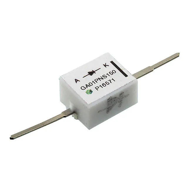
GA01PNS150-220
Silicon Carbide
PiN Diode
Features
A
15 kV blocking
250 °C operating temperature
Fast turn off characteristics
Soft reverse recovery characteristics
Ultra-Fast high temperature switching
K
Advantages
Applications
Industry’s first > 10 kV power rectifier
Reduced stacking
Reduced system complexity/Increased reliability
Voltage Multiplier
Ignition/Trigger Circuits
Oil/Downhole
Lighting
Defense
Maximum Ratings at Tj = 250 °C, unless otherwise specified
Parameter
Repetitive peak reverse voltage
Continuous forward current
RMS forward current
Operating and storage temperature
Symbol
VRRM
IF
IF(RMS)
Tj , Tstg
Conditions
Values
15
1
0.5
-55 to 250
TC ≤ 150 °C
TC ≤ 150 °C
Unit
kV
A
A
°C
Electrical Characteristics at Tj = 250 °C, unless otherwise specified
Parameter
Symbol
Diode forward voltage
VF
Reverse current
IR
Total reverse recovery charge
Qrr
Switching time
ts
Total capacitance
C
Total capacitive charge
QC
Conditions
min.
IF = 1 A, Tj = 25 °C
IF = 1 A, Tj = 225 °C
VR = 15 kV, Tj = 25 °C
VR = 15 kV, Tj = 225 °C
VR = 1000 V
IF ≤ IF,MAX
IF = 1.5 A
dIF/dt = 70 A/μs
VR = 1000 V
Tj = 225 °C
IF = 1.5 A
VR = 1 V, f = 1 MHz, Tj = 25 °C
VR = 400 V, f = 1 MHz, Tj = 25 °C
VR = 1000 V, f = 1 MHz, Tj = 25 °C
VR = 1000 V, f = 1 MHz, Tj = 25 °C
Values
typ.
6.5
4.4
1
5
max.
7.0
5.0
20
100
Unit
V
µA
558
nC
< 236
ns
28
8
7
5.34
pF
nC
Sep 2014
http://www.genesicsemi.com/commercial-sic/sic-ultra-high-voltage-pin-thyristors
Page 1 of 3
�
Figure 1: Typical Forward Characteristics
Figure 2: Typical Reverse Characteristics
Figure 3: Typical Junction Capacitance vs Reverse Voltage
Characteristics
Figure 4: Typical Turn Off Characteristics at Ik = 0.5 A and
VR = 1000 V
Figure 5: Typical Turn Off Characteristics at Tj = 225 °C and
VR = 1000 V
Figure 6: Reverse Recovery Charge vs Cathode Current
Sep 2014
GA01PNS150-220
http://www.genesicsemi.com/commercial-sic/sic-ultra-high-voltage-pin-thyristors
Page 2 of 3
�GA01PNS150-220
Figure 7: Reverse Recovery Time vs Cathode Current
Revision History
Date
Revision
Comments
2014/09/15
0
Initial release
Supersedes
Published by
GeneSiC Semiconductor, Inc.
43670 Trade Center Place Suite 155
Dulles, VA 20166
GeneSiC Semiconductor, Inc. reserves right to make changes to the product specifications and data in this document without notice.
GeneSiC disclaims all and any warranty and liability arising out of use or application of any product. No license, express or implied to any
intellectual property rights is granted by this document.
Unless otherwise expressly indicated, GeneSiC products are not designed, tested or authorized for use in life-saving, medical, aircraft
navigation, communication, air traffic control and weapons systems, nor in applications where their failure may result in death, personal
injury and/or property damage.
Sep 2014
http://www.genesicsemi.com/commercial-sic/sic-ultra-high-voltage-pin-thyristors
Page 3 of 3
�
GA01PNS150-CAU
SPICE Model Parameters
Copy the following code into a SPICE software program for simulation of the GA01PNS150-220 device.
*
MODEL OF GeneSiC Semiconductor Inc.
*
*
$Revision:
1.0
$
*
$Date:
15-SEP-2014
$
*
*
GeneSiC Semiconductor Inc.
*
43670 Trade Center Place Ste. 155
*
Dulles, VA 20166
*
http://www.genesicsemi.com/index.php/hit-sic/baredie
*
*
COPYRIGHT (C) 2014 GeneSiC Semiconductor Inc.
*
ALL RIGHTS RESERVED
*
* These models are provided "AS IS, WHERE IS, AND WITH NO WARRANTY
* OF ANY KIND EITHER EXPRESSED OR IMPLIED, INCLUDING BUT NOT LIMITED
* TO ANY IMPLIED WARRANTIES OF MERCHANTABILITY AND FITNESS FOR A
* PARTICULAR PURPOSE."
* Models accurate up to 2 times rated drain current.
*
* Start of GA01PNS150-220 SPICE Model
*
.MODEL GA01PNS150 D
+ IS
9.71E-12
+ RS
2.07
+ N
5.7869
+ IKF
0.039646
+ EG
3.23
+ XTI
58
+ TRS1
-0.0034
+ CJO
2.28E-11
+ VJ
2.304
+ M
0.376
+ FC
0.5
+ BV
16000
+ IBV
1.00E-03
+ VPK
15000
+ IAVE
1
+ TYPE
SiC_PiN
+ MFG
GeneSiC_Semi
*
* End of GA01PNS150-220 SPICE Model
Sep 2014
http://www.genesicsemi.com/commercial-sic/sic-ultra-high-voltage-pin-thyristors
Page 1 of 1
�
很抱歉,暂时无法提供与“GA01PNS150-220”相匹配的价格&库存,您可以联系我们找货
免费人工找货