TPH3205WSBQA
Not recommended for new designs—see TP65H050WSQA
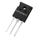
AEC-Q101 Qualified 650V GaN FET in TO-247 (source tab)
Description
Features
The TPH3205WSBQA 650V, 49mΩ Gallium Nitride (GaN)
FET is a normally-off automotive (AEC-Q101) qualified
device. It combines state-of-the-art high voltage GaN HEMT
and low voltage silicon MOSFET technologies—offering
superior reliability and performance.
Transphorm GaN offers improved efficiency over silicon,
through lower gate charge, lower crossover loss, and smaller
reverse recovery charge.
Related Literature
AN0009: Recommended External Circuitry for GaN FETs
AN0003: Printed Circuit Board Layout and Probing
AN0010: Paralleling GaN FETs
Ordering Information
Part Number
Package
Package
Configuration
TPH3205WSBQA
3 lead TO-247
Source
TPH3205WSBQA
TO-247
(top view)
S
JEDEC and AEC-Q101 qualified GaN technology
Dynamic RDS(on)eff production tested
Robust design, defined by
— Intrinsic lifetime tests
— Wide gate safety margin
— Transient over-voltage capability
Very low QRR
Reduced crossover loss
RoHS compliant and Halogen-free packaging
Benefits
Enables AC-DC bridgeless totem-pole PFC designs
— Increased power density
— Reduced system size and weight
— Overall lower system cost
Achieves increased efficiency in both hard- and softswitched circuits
Easy to drive with commonly-used gate drivers
GSD pin layout improves high speed design
Applications
Automotive
Datacom
Broad industrial
PV inverter
Servo motor
Key Specifications
G
VDSS (V)
650
V(TR)DSS (V)
800
RDS(on)eff (mΩ) max*
S
D
62
QRR (nC) typ
136
QG (nC) typ
28
* Dynamic on-resistance; see Figures 19 and 20
Common Topology Power Recommendations
Cascode Schematic Symbol
Cascode Device Structure
CCM bridgeless totem-pole*
2983W max
Hard-switched inverter**
3581W max
Conditions: FSW=45kHz; TJ=115°C; THEATSINK=90°C; insulator between
device and heatsink (6 mil Sil-Pad® K-10); power de-rates at lower
voltages with constant current
*
VIN=230VAC; VOUT=390VDC
** VIN=380VDC; VOUT=240VAC
October 31, 2019
tph3205wsbqa.2
© 2017 Transphorm Inc. Subject to change without notice.
1
�TPH3205WSBQA
Absolute Maximum Ratings (Tc=25°C unless otherwise stated.)
Symbol
VDSS
Parameter
Limit Value
Unit
Drain to source voltage (TJ = -55°C to 150°C)
650
Transient drain to source voltage a
800
Gate to source voltage
±18
Maximum power dissipation @TC=25°C
125
W
Continuous drain current @TC=25°C b
35
A
Continuous drain current @TC=100°C b
22
A
Pulsed drain current (pulse width: 10µs)
150
A
(di/dt)RDMC
Reverse diode di/dt, repetitive c
1500
A/µs
(di/dt)RDMT
Reverse diode di/dt, transient d
2900
A/µs
Case
-55 to +150
°C
Junction
-55 to +150
°C
-55 to +150
°C
260
°C
Typical
Unit
1
°C/W
40
°C/W
V(TR)DSS
VGSS
PD
ID
IDM
TC
TJ
TS
TSOLD
Operating temperature
Storage temperature
Soldering peak temperature e
V
Notes:
a. In off-state, spike duty cycle D
很抱歉,暂时无法提供与“TPH3205WSBQA”相匹配的价格&库存,您可以联系我们找货
免费人工找货