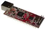
DLP2232MSPF
LEAD FREE
USB / MICROCONTROLLER MODULE
The DLP-2232MSPF combines the same USB interface used in the DLP-2232H and the DLP-1232H
modules with a Texas Instruments microcontroller with internal FRAM to form a rapid development
tool. The MSP430FR5739 microcontroller is preprogrammed with basic functionality for accessing the
port pins and can be reprogrammed with user firmware via a 12-pin header using the
MSP-FET430UIF device programmer/debugger (purchased separately).
FEATURES:
•
The DLP-2232MSPF module utilizes a Texas Instruments 16-bit RISC architecture processor with
16K bytes FRAM, 1K bytes RAM and a multi-channel,10-bit A/D converter
‐ Up to 24MHz operation
‐ Ultra low power FRAM operates as unified memory and is configurable as code, data or
storage memory
‐ FRAM write access and code execution at up to 24MHz
‐ FRAM has virtually unlimited write endurance (1014 cycles)
‐ FRAM is inherently secure and radiation resistant
•
The DLP-2232MSPF has 26 digital I/O lines available for interfacing to user electronics via a
compact, 40-pin DIP footprint module (12 can be configured as A/D inputs)
•
Send/receive data over a high-speed USB 2.0 interface to a host computer at 1M baud (921600)
•
Required 5V power supply can be taken directly from the USB port or supplied by user electronics
•
“Token I/O” code is preprogrammed into the MSP430FR5739’s FRAM memory for basic port pin
input/output capability including access to the A/D converter
•
The FRAM memory can be easily erased and reprogrammed utilizing a user-supplied compatible
programmer or a user-supplied internal bootstrap loader through UART UCA0
•
No in-depth knowledge of USB is required as all USB protocols are handled automatically by the
on-board FT2232H and its support circuitry
‐
‐
‐
‐
Royalty-free device drivers eliminate the need for USB driver development in most cases
USB bulk or isochronous data-transfer modes
USB 1.1 and USB 2.0 compatible
USB VID, PID, serial number and product-description strings are stored in on-board EEPROM
memory
Rev. 1.1 (November 2011)
1
© DLP Design, Inc.
�APPLICATION AREAS:
•
•
•
•
•
•
•
•
•
•
Prototype development
USB ISDN and ADSL modems
USB interface for digital cameras
USB interface for MP3 players
High-speed USB instrumentation
USB smart-card readers
Set top box (STB) PC-USB interface
USB hardware modems
USB wireless modems
USB bar code readers
1.0 GENERAL DESCRIPTION
The DLP-2232MSPF provides a cost-effective, microcontroller-based method of interfacing an
electronic peripheral to a host computer via USB.
To send data from the peripheral to the host computer, the microcontroller simply writes data into the
FT2232H on its RXD pin at 1M baud. Commands and data sent from the host are transferred serially
on the TXD pin.
By using FTDI’s Virtual COM Port Drivers, the peripheral looks like a standard COM port to the
application software. The latest versions of the drivers are available for download from DLP Design’s
website at www.dlpdesign.com.
2.0 DRIVER SOFTWARE
FTDI's VCP (Virtual COM Port) driver-executable files are provided royalty free on the condition that
they are used only with designs incorporating an FTDI device (i.e. the FT2232H on the
DLP-2232MSPF). The latest version of the drivers can be downloaded from www.dlpdesign.com or
www.ftdichip.com.
The VCP driver download file is a combined set of drivers for Windows 7, Windows Vista and
Windows 2000/XP. Unzip the file to a blank floppy disk or folder on your PC. (The drivers can coexist
on the same floppy disk or folder since the INF files determine which set of drivers to load for each
operating system version.) Once loaded, the VCP drivers allow the application software running on
your host PC to communicate with the DLP-2232MSPF as though it were connected to a COM
(RS-232) port.
In addition to VCP drivers, FTDI's D2XX direct drivers offer an alternative solution to the VCP drivers
that allow application software to interface with the DLP-2232MSPF using a DLL instead of a Virtual
COM Port. The architecture of the D2XX drivers consists of a Windows WDM driver that communicates with the device via the Windows USB stack and a DLL that interfaces the application software
(written in VC++, C++ Builder, Delphi, VB, etc.) to the WDM driver.
The D2XX direct drivers add support for simultaneous access and control of multiple FT2232H
devices. The extended open function (FT_OpenEx) allows the device to be opened by either its
product description or serial number, both of which can be programmed to be unique. The List
Rev. 1.1 (November 2011)
2
© DLP Design, Inc.
�Devices function (FT_ListDevices) allows the application software to determine which devices are
currently available for use, again by product description or by serial number.
Download FTDI Application Notes AN232-03, AN232-05, AN232-06 and AN232-07 for detailed
instructions on how to install and remove the drivers.
3.0 EEPROM WRITE UTILITY
The DLP-2232MSPF has the option to accept manufacturer-specific information that is written into onboard EEPROM memory. Parameters that can be programmed include the VID and PID identifiers,
the manufacturer's product string or a serial number.
MPROG is an EEPROM serializer from FTDI for the FT2232H device. MPROG is based on the new
D2XX drivers and will work on Windows 7, Windows Vista and Windows 2000/XP platforms.
You must install the latest release of the CDM drivers in order to run this application. (Refer to
the MPROG User’s Guide for details on the program’s use.)
4.0 QUICK START GUIDE
This guide requires the use of a Windows 7/Vista/2000/XP PC that is equipped with a USB port.
1. Download the WHQL-certified CDM device drivers from either www.dlpdesign.com or
www.ftdichip.com. Unzip the drivers onto a blank floppy disk or into a folder on the hard drive.
Note: The DLP-2232MSPF can be configured to receive its operating power from the USB port or
from user electronics. Pins 19 and 20 allow for this configuration. (Refer to the Pinout Description
in the next section for details on the DLP-2232MSPF electrical interface.)
**The board will not operate until a power source has been connected.**
2. Connect the DLP-2232MSPF board to the PC via a standard A-B, 6-foot USB cable. This action
initiates loading of the USB drivers. When prompted, select the folder where the CDM device
drivers were stored in Step 1. Windows will then complete the installation of the device drivers for
the DLP-2232MSPF board. The next time the DLP-2232MSPF board is attached, the host PC will
immediately load the correct drivers without any prompting. Reboot the PC if prompted to do so.
The DLP-2232MSPF is shipped with default VID, PID, etc. values programmed into the
EEPROM memory. You only need to run MPROG if you want to change the default values.
At this point, the DLP-2232MSPF is ready for use. Note that the DLP-2232MSPF will appear
non-responsive if data sent from the host PC is not read from the FT2232H device by the
MSP430FR5739 microcontroller. The token firmware with which the DLP-2232MSPF comes
preloaded will read data sent by the host by default. Custom user firmware should also follow this
protocol.
Rev. 1.1 (November 2011)
3
© DLP Design, Inc.
�5.0 TOKEN I/O
The MSP430FR5739 microcontroller on the DLP-2232MSPF comes preprogrammed with firmware
that provides rudimentary access to the port pins via either the VCP or DLL drivers. Features include
the ability to read and write individual port pins.
The firmware in the DLP-2232MSPF also provides access to the MSP430FR5739’s A/D converter
and communications. Commands sent to the Token I/O firmware must adhere to a specific
communications protocol. Each command sequence contains the following information:
Byte 0:
Byte 1:
Byte 2…n:
Number of bytes in command sequence
Command
Parameter/data bytes
For example, setting Port Pin P1.1 high would require the following string of bytes:
0x05, 0x30, 0x11, 0x00, 0x01
Definition of the Bytes:
0x05 – Number of bytes in command
0x30 – Command for digital port-pin access
0x11 – Affected port pin
0x00 – Set port pin to output
0x01 – Desired state of port pin
The port pins equate to hexadecimal numeric constants as defined here:
PORT 1:
0x10 = P1.0 MSP430FR5739 Pin 1, DLP-2232MSPF module Pin J1.2
0x11 = P1.1 MSP430FR5739 Pin 2, DLP-2232MSPF module Pin J1.1
0x12 = P1.2 MSP430FR5739 Pin 3, DLP-2232MSPF module Pin J1.4
0x13 = P1.3 MSP430FR5739 Pin 8, DLP-2232MSPF module Pin J1.5
0x14 = P1.4 MSP430FR5739 Pin 9, DLP-2232MSPF module Pin J1.6
0x15 = P1.5 MSP430FR5739 Pin 10, DLP-2232MSPF module Pin J1.7
0x16 = P1.6 MSP430FR5739 Pin 28, DLP-2232MSPF module Pin J1.35
0x17 = P1.7 MSP430FR5739 Pin 29, DLP-2232MSPF module Pin J1.34
PORT 2:
0x22 = P2.2 MSP430FR5739 Pin 23, DLP-2232MSPF module Pin J1.26
0x23 = P2.3 MSP430FR5739 Pin 34, DLP-2232MSPF module Pin J1.38
0x24 = P2.4 MSP430FR5739 Pin 35, DLP-2232MSPF module Pin J1.39
0x27 = P2.7 MSP430FR5739 Pin 33, DLP-2232MSPF module Pin J1.37
Rev. 1.1 (November 2011)
4
© DLP Design, Inc.
�PORT 3:
0x30 = P3.0 MSP430FR5739 Pin 4, DLP-2232MSPF module Pin J1.17
0x31 = P3.1 MSP430FR5739 Pin 5, DLP-2232MSPF module Pin J1.16
0x32 = P3.2 MSP430FR5739 Pin 6, DLP-2232MSPF module Pin J1.14
0x33 = P3.3 MSP430FR5739 Pin 7, DLP-2232MSPF module Pin J1.15
0x34 = P3.4 MSP430FR5739 Pin 24, DLP-2232MSPF module Pin J1.28
0x35 = P3.5 MSP430FR5739 Pin 25, DLP-2232MSPF module Pin J1.30
0x36 = P3.6 MSP430FR5739 Pin 26, DLP-2232MSPF module Pin J1.29
0x37 = P3.7 MSP430FR5739 Pin 27, DLP-2232MSPF module Pin J1.31
PORT 4:
0x40 = P4.0 MSP430FR5739 Pin 15, DLP-2232MSPF module Pin J1.23
0x41 = P4.1 MSP430FR5739 Pin 16, DLP-2232MSPF module Pin J1.24
PORT J:
0x50 = PJ.0/TDO MSP430FR5739 Pin 11, DLP-2232MSPF module Pin J1.10
0x51 = PJ.1/TDI MSP430FR5739 Pin 12, DLP-2232MSPF module Pin J1.9
0x52 = PJ.2/TMS MSP430FR5739 Pin 13, DLP-2232MSPF module Pin J1.12
0x53 = PJ.3/TCK MSP430FR5739 Pin 14, DLP-2232MSPF module Pin J1.11
The source code for the Token I/O firmware (developed using Code Composer) is available as a free
download upon purchase and receipt of the hardware. Example Visual C++ source code developed
using Microsoft Visual C for communicating with the DLP-2232MSPF via the Token I/O firmware is
also available for download.
5.1 TOKEN I/O COMMAND SET
0x27 – Ping – Host Notification
Length:
Parameters:
Returns:
Function:
Example:
2 Bytes
None
1 Byte: ASCII “F” or hex 0x46
This function returns an ASCII “F” to tell the host that the module is up and running
0x02, 0x27 – Causes the module to return a 0x53 to the host
0x28 – Flash LED – Toggle the LED
Length:
Parameters:
Returns:
Function:
Example:
2 Bytes
None
1 Byte: Command echo acknowledgement=0x28
This function will cause the module’s green LED to flash briefly
0x02, 0x28 – Causes the LED to toggle briefly
0x29 – LED On/Off
Length:
Parameters:
Returns:
Function:
Example:
3 Bytes
1 Byte: 0=Turn LED Off; 1=Turn LED On
1 Byte: Command echo acknowledgement=0x29
This function will turn the module’s green LED on or off
0x03, 0x29, 0x01 – Turns on the LED
Rev. 1.1 (November 2011)
5
© DLP Design, Inc.
�0x30 – Digital I/O Read/Write
Length:
4 or 5 Bytes
Parameters: 2 or 3 Bytes:
1. Port Selection – Select the desired MSP430FR5739 port pin (refer to the port list on
the previous page)
2. Port Direction: 1=Input; 0=Output
3. Port Value if Byte 2 specifies Output
Returns:
2 Bytes for Input=Value on port pin; command echo acknowledgement=0x30
1 byte for Output=command echo acknowledgement=0x30
Function:
This function will read from or write to the selected port pin
Example:
0x04, 0x30, 0x60, 0x00, 0x01 – Sets Port 6 Pin 0 high
0x40 – A/D Conversion
Length:
3 Bytes
Parameters: Mode: 0=Single conversion, 1=Continuous conversions (~1 per second)
Note: Setting the ADC mode to continuous (1) starts an infinite loop. The ADC
will perform a conversion approximately twice a second and report the result to
the host. To exit, stop the code execution using the debugger, or reset the
module by unplugging the USB cable and then reconnecting it.
Returns:
Function:
Example:
2 Bytes: The 10-bit voltage data; MSB first
This function will enable A/D conversion on the selected channel and ADC, pause
10uS, perform the A/D conversion and then return 2 bytes to the host (MSB first).
Command 0x42 must have been previously called to configure the desired analog
channel as an A/D input, and 0x43 / 0x44 must have been called to configure the
voltage reference.
0x3, 0x40 0x00 – Performs the A/D conversion and, using ADC0, returns 2 bytes of
data followed by an echo of the command byte sent.
0x41 – Disable A/D
Length:
Parameters:
Returns:
Function:
Example:
2 Bytes
None
1 Byte: command echo acknowledgement=0x41
This function disables the A/D converter
0x2, 0x41 – Disables A/D Converter
Rev. 1.1 (November 2011)
6
© DLP Design, Inc.
�0x42 – Select A/D Input
Length:
3 Bytes
Parameters: 0x00=Select Input A0 (P1.0)
0x01=Select Input A1 (P1.1)
0x02=Select Input A2 (P1.2)
0x03=Select Input A3 (P1.3)
0x04=Select Input A4 (P1.4)
0x05=Select Input A5 (P1.5)
0x06=Select Input A6 (P1.6)
0x07=Select Input A7 (P1.7)
0x08=Select Input Veref+
0x09=Select Internal Input Vref-/Veref0x0A=Select Internal Temperature Diode
0x0B=Select Internal Input (Avcc – Avss)/2
Returns:
1 Byte: command echo acknowledgement=0x42
Function:
This function selects the analog input to be used by the specified A/D converter
Example:
0x3, 0x42 0x03 – Selects Analog Input A3
0x43 – Select Reference Source
Length:
3 Bytes
Parameters: 0x00=Select Reference AVCC & AVSS
0x01=Select Reference VREF & AVSS (refer to command 0x44 to configure VREF)
0x02=Select Reference VEREF+ buffered & AVSS
0x03=Select Reference VEREF+ & AVSS
0x04=Select Reference AVCC & VEREF0x05=Select Reference VREF & VEREF- (refer to command 0x44 to configure VREF)
0x06=Select Reference VEREF+ buffered & VEREF0x07=Select Reference VEREF+ & VEREFReturns:
1 Byte: command echo acknowledgement=0x43
Function:
This function sets the A/D and D/A references to be external
Example:
0x2, 0x43, 0x01 – Select the Internal Voltage Reference VREF as the source
0x44 – Internal Reference Voltage
Length:
Parameters:
Returns:
Function:
Example:
3 Bytes
0 = +1.0V; 1 = +2.0V; 2 = +2.5V
1 Byte: command echo acknowledgement=0x44
This function sets the A/D and D/A references to be internal; use command 0x50 to
select the Internal Voltage Reference value
0x2, 0x44, 0x01 – Select Internal Voltage Reference of +2.0V
Rev. 1.1 (November 2011)
7
© DLP Design, Inc.
�TABLE 1: DLP-2232MSPF PINOUT DESCRIPTION
(Top View)
1
20
PIN #
1
2
3
4
5
6
7
8
9
10
11
12
13
40 Pin,
.6 inch
Header
USB 'B'
Type
Connector
40
21
DESCRIPTION
P1.1/A1/VeREF+ (I/O) Port 1 Pin 1 connected to the MSP430FR5739 Digital I/O P1.1,
Analog Input 1 and the positive External Voltage Reference input
P1.0/A0/VeREF- (I/O) Port 1 Pin 0 connected to the MSP430FR5739 Digital I/O P1.0,
Analog Input 0 and the negative External Voltage Reference input
GROUND
P1.2/A2 (I/O) Port 1 Pin 2 connected to the MSP430FR5739 Digital I/O P1.2 and Analog
Input 2
P1.3/A3 (I/O) Port 1 Pin 3 connected to the MSP430FR5739 Digital I/O P1.3 and Analog
Input 3
P1.4/A4 (I/O) Port 1 Pin 4 connected to the MSP430FR5739 Digital I/O P1.4 and Analog
Input 4
P1.5/A5 (I/O) Port 1 Pin 5 connected to the MSP430FR5739 Digital I/O P1.5 and Analog
Input 5
GROUND
PJ.1/TDI (I/O) Port J Pin 1 connected to the MSP430FR5739 Digital I/O PJ.1 and the
JTAG Test Data Input
PJ.0/TDO (I/O) Port J Pin 0 connected to the MSP430FR5739 Digital I/O PJ.0 and the
JTAG Test Data Output
PJ.3/TCK (I/O) Port J Pin 3 connected to the MSP430FR5739 Digital I/O PJ.3 and the
JTAG Test Clock
PJ.2/TMS (I/O) Port J Pin 2 connected to the MSP430FR5739 Digital I/O PJ.2 and the
JTAG Test Mode Select
GROUND
Rev. 1.1 (November 2011)
8
© DLP Design, Inc.
�14
15
16
17
18
19
20
21
22
23
24
25
26
27
28
29
30
31
32
33
34
35
36
37
38
39
40
P3.2/A14 (I/O) Port 3 Pin 2 connected to the MSP430FR5739 Digital I/O P3.2 and
Analog Input 14
P3.3/A15 (I/O) Port 3 Pin 3 connected to the MSP430FR5739 Digital I/O P3.3 and
Analog Input 15
P3.1/A13 (I/O) Port 3 Pin 1 connected to the MSP430FR5739 Digital I/O P3.1 and
Analog Input 13
P3.0/A12 (I/O) Port 3 Pin 0 connected to the MSP430FR5739 Digital I/O P3.0 and
Analog Input 12
GROUND
EXTVCC (In) Use for applying main power (4.4-5.25 volts) to the module; connect to
PORTVCC if the module is to be powered by the USB port (typical configuration)
PORTVCC (Out) Power from USB port—Connect to EXTVCC if the module is to be
powered by the USB port (typical configuration); 500mA is the maximum current
available to the DLP-2232MSPF and target electronics if the USB device is configured for
high power
VCCUSB (Out) Power from EXTVCC (Pin 20) through the on-board filter
GROUND
P4.0 (I/O) Port 4 Pin 0 connected to the MSP430FR5739 Digital I/O P4.0
P4.1 (I/O) Port 4 Pin 1 connected to the MSP430FR5739 Digital I/O P4.1 and the
module’s on-board LED
GROUND
P2.2 (I/O) Port 2 Pin 2 connected to the MSP430FR5739 Digital I/O P2.2
GROUND
P3.4 (I/O) Port 3 Pin 4 connected to the MSP430FR5739 Digital I/O P3.4
P3.6 (I/O) Port 3 Pin 6 connected to the MSP430FR5739 Digital I/O P3.6
P3.5 (I/O) Port 3 Pin 5 connected to the MSP430FR5739 Digital I/O P3.5
P3.7 (I/O) Port 3 Pin 7 connected to the MSP430FR5739 Digital I/O P3.7
RESETMSPn (Active Low Input) connected to the active low /RST pin of the
MSP430FR5739. This input is pulled high on the module.
GROUND
P1.7/A7 (I/O) Port 1 Pin 7 connected to the MSP430FR5739 Digital I/O P1.7 and Analog
Input 7
P1.6/A6 (I/O) Port 1 Pin 6 connected to the MSP430FR5739 Digital I/O P1.6 and Analog
Input 6
GROUND
P2.7 (I/O) Port 2 Pin 7 connected to the MSP430FR5739 Digital I/O P2.7
P2.3/A6 (I/O) Port 2 Pin 3 connected to the MSP430FR5739 Digital I/O P2.3 and Analog
Input 6
P2.4/A7 (I/O) Port 2 Pin 4 connected to the MSP430FR5739 Digital I/O P2.4 and Analog
Input 7
GROUND
Rev. 1.1 (November 2011)
9
© DLP Design, Inc.
�6.0
MECHANICAL DRAWINGS (PRELIMINARY) INCHES (MILLIMETERS)
UNLESS OTHERWISE NOTED
0.25 typ.
( 6.4typ.)
2.38 typ.
(60.5 typ.)
0.1 typ.
(2.54 typ.)
0.25 typ.
(6.4 typ.)
0.25 typ.
(6.4typ.)
0.48 typ.
(12.2 typ.)
0.50 typ.
(12.7 typ.)
0.6 typ.
(15.2 typ.)
0.018 x 0.018 typ. square
(0.46 x 0.46 typ.) pin
0.6 typ.
(15.2 typ.)
0.38 typ.
(9.7 typ.)
0.89 typ.
(22.6 typ.)
Rev. 1.1 (November 2011)
0.65 typ.
(16.5 typ.)
10
© DLP Design, Inc.
�7.0 DISCLAIMER
Neither the whole nor any part of the information contained within or the product described in this
datasheet may be adapted or reproduced in any material or electronic form without the prior written
consent of the copyright holder.
This product and its documentation are supplied on an as-is basis, and no warranty as to their
suitability for any particular purpose is either made or implied. DLP Design will not accept any claim
for damages whatsoever arising as a result of use or failure of this product. Your statutory rights are
not affected.
This product or any variant of it is not intended for use in any medical appliance, device or system in
which the failure of the product might reasonably be expected to result in personal injury.
This document provides preliminary information that may be subject to change without notice.
8.0 CONTACT INFORMATION
DLP Design, Inc.
1605 Roma Lane
Allen, TX 75013
Email:
Internet:
support@dlpdesign.com
http://www.dlpdesign.com
Rev. 1.1 (November 2011)
11
© DLP Design, Inc.
�D
1
6
3
2
5
U2
NCP605-3.3V
VIN VOUT
VIN
EN SENSE
1
2
3
4
GND
U3
CS
SK
DIN
DOUT
10K
4
5
P3V3
2
C8
EECS
EESK
EEDATA
C11
4.7uF .1uF
C12
C13
C10
.1uF
P3V3
C7
.1uF
P5V0
C3
.1uF
R6
10K
C23
27pF
C22
27pF
P3V3
Y1
12MHz
R5
10K
R4
12K
R3
1K
.1uF
C1
10/10 Tant
FB1
240-1018-1
10uF/10V
1
C2
.01
1
2
3
4
R2
2K2
4
VPLL
VPHY
4
TEST
P3V3
ADBUS0/TXD/D0/TCK SK
ADBUS1/RXD/D1/TDI DO
ADBUS2/RTS#/D2/TDO DI
ADBUS3/CTS#/D3/TMS CS
ADBUS4/DTR#/D4/GPIOL0
ADBUS5/DSR#/D5/GPIOL1
ADBUS6/DCD#/D6/GPIOL2
ADBUS7/RI#/D7/GPIOL3
ACBUS0/TXDEN/RXF#/GPIOH0
ACBUS1/WRSTB#/TXE#/GPIOH1
ACBUS2/RDSTB#/RD#/GPIOH2
ACBUS3/TXLED#/WR#/GPIOH3
ACBUS4/RXLED#/SIWUA/GPIOH4
ACBUS5/-/CLKOUT/GPIOH5
ACBUS6/-/OE#/GPIOH6
ACBUS7/-/-/GPIOH7
BDBUS0/TXD/DO/TCK SK
BDBUS1/RXD/D1/TDI DO
BDBUS2/RTS#/D2/TDO DI
BDBUS3/CTS#/D3/TMS CS
BDBUS4/DTR#/D4/GPIOL0
BDBUS5/DSR#/D5/GPIOL1
BDBUS6/DCD#/D6/GPIOL3
BDBUS7/RI#/D7/GPIOL4
PWREN#
SUSPEND#
BCBUS0/TXDEN/RXF#/GPIOH0
OSCI
BCBUS1/WRSTB#/TXE#/GPIOH1
BCBUS2/RDSTB#/RD#/GPIOH2
BCBUS3/TXLED#/WR#/GPIOH3
BCBUS4/RXLED#/SIWUB/GPIOH4
OSCO
BCBUS5/-/-/GPIOH5
BCBUS6/-/-/GPIOH6
BCBUS7/PWRSAV#/PWRSAV#/GPIOH7
EECS
EECLK
EEDATA
DM
DP
RESET#
REF
VREGOUT
VREGIN
U1
FT1232HQ
50
49
14
6
7
8
63
62
61
2
3
13
20
31
42
56
P5V0
CN1
CN-USB
8
7
6
5
VCC
NC
NC/ORG
GND
93LC46
R1
R7
0
PORTVCC
EXTVCC
C6
1.0uF/0603
P3V3
C9
.1uF
DLP-2232MSPF
v1.0
5
C14
.1uF
C15
.1uF
C16
.1uF
C17
3
1
3
2
C25
.1uF
1
2
J2
J3
JTAG HEADER
11
9
7
5
3
1
RESETMSPn
2
R11
10
VCCMSP
C30
.1uF
C31
2.2uF/0603
C5
470nF
C4
.1uF
1
21
22
23
34
35
17
18
33
P2.4/A7
P2.3/A6
P2.7
P1.6/A6
P1.7/A7
RESETMSPn
P3.7
P3.5
P3.6
P3.4
P2.2
P4.1/LED#
P4.0
VCCUSB
1
VCCMSP
15
16
RST/NIM/SBWTDIO
P2.0/TB2.0/UCA0TXD/UCA0SIMO/TB0CLK/ACLK
PJ.3/TCK/CD9
P2.1/TB2.1/UCA0RXD/UCASOMI/TB0.0
PJ.2/TMS/TB2OUTH/ACLK/CD8
P2.2/TB2.2/UCB0CLK/TB1.0
PJ.1/TDI/TCLK/TB1OUTH/MCLK/CD7
P2.3/TA0.0/UCA1STE/A6/CD10
PJ.0/TDO/TB0OUTH/SMCLK/CD6
P2.4/TA1.0/UCA1CLK/A7/CD11
P2.5/TB0.0/UCA1TXD/UCA1SIMO
TEST/SBWTCK
P2.6/TB1.0/UCA1RXD/UCA1SOMI
P2.7
VCCUSB
J1
CONN PCB 20x2
1 1
40 40
2
2
39 39
3 3
38 38
4 4
37 37
5 5
36 36
6 6
35 35
7 7
34 34
8 8
33 33
9
9
32 32
10 10
31 31
11 11
30 30
12 12
29 29
13 13
28 28
14
14
27 27
15 15
26 26
16
16
25 25
17 17
24 24
18 18
23 23
19 19
22 22
20 20
21 21
P5V0
P4.0/TB2.0
P4.1
4
5
6
7
24
25
26
27
PJ.4/XIN
PJ.5/XOUT
P1.0/TA0.1/DMAE0/RTCCLK/AO/CD0/VeREFP1.1/TA0.2/TA1CLK/CDOUT/A1/CD1/VeREF+
P3.0/A12/CD12
P1.2/TA1.1/TA0CLK/CDOUT/A2/CD2
P3.1/A13/CD13
P1.3/TA1.2/UCB0STE/A3/CD3
P3.2/A14/CD14
P1.4/TB0.1/UCA0STE/A4/CD4
P3.3/A15/CD15
P1.5/TB0.2/UCA0CLK/A5/CD5
P3.4/TB1.1/TB2CLK/SMCLK
P1.6/TB1.1/UCB0SIMO/UCB0SDA/TA0.0
P3.5/TB1.2/CDOUT
P1.7/TB1.2/UCB0SOMI/UCB0SCL/TA1.0
P3.6/TB2.1/TB1CLK
P3.7/TB2.2
U4
MSP430FR5739IRHA
R10
47K
20
14
13
12
11
19
1
2
3
8
9
10
28
29
37
38
2
EXTVCC
PORTVCC
P3.2/A14
P3.3/A15
P3.1/A13
P3.0/A12
PJ.1/TDI
PJ.0/TDO
PJ.3/TCK
PJ.2/TMS
P1.2/A2
P1.3/A3
P1.4/A4
P1.5/A5
P1.1/A1/VeREF+
P1.0/A0/VeREF-
VCCSW
RESETMSPn
TCK
TMS
TDI
TDO
TEST
Y2
24.0MHz
P1.0/A0/VeREFP1.1/A1/VeREF+
P1.2/A2
P1.3/A3
P1.4/A4
P1.5/A5
P1.6/A6
P1.7/A7
PJ.3/TCK
PJ.2/TMS
PJ.1/TDI
PJ.0/TDO
C26
18pF
C27
18pF
VCCSW
VPLL
VPHY
C29
4.7uF
12
10
8
6
4
2
1X2HDR
.1uF
C21
.1uF
C19
C28
.1uF
RESETMSPn
TEST
Q2
MMBT3904
TEST
VCCMSP
R8
10K
P2.6/UCA1RXD
P2.5/UCA1TXD
C24
.1uF
0
0
P2.1/UCAORXD
P2.0/UCAOTXD
R13
R12
2
FB2
240-1018-1
Q1
IRLML6402 1
P3V3
3
R9
2.2K
2
RESETMSPn
.1uF
16
17
18
19
21
22
23
24
26
27
28
29
30
32
33
34
38
39
40
41
43
44
45
46
48
52
53
54
55
57
58
59
60
36
P3V3
1
C18
4.7uF/10V
C20
2
4.7uF/10V
FB3
240-1018-1
1
3
VCORE
40
AVCC
32
DVCC
30
AVSS
AVSS
VCCIO
VCCIO
VCCIO
VCCIO
GND
GND
GND
GND
GND
GND
GND
GND
39
36
12
37
64
1
5
11
15
25
35
47
51
DVSS
VCORE
VCORE
VCORE
AGND
31
4
9
VPHY
VPLL
10
C
B
A
5
P2.0/UCAOTXD
P2.1/UCAORXD
P2.2
P2.3/A6
P2.4/A7
P2.5/UCA1TXD
P2.6/UCA1RXD
P2.7
P3.0/A12
P3.1/A13
P3.2/A14
P3.3/A15
P3.4
P3.5
P3.6
P3.7
P4.0
P4.1/LED#
LNJ306G5TR02
D1
360
R14
D
C
B
A
�