PJM3400NSC
N- Enhancement Mode Field Effect Transistor
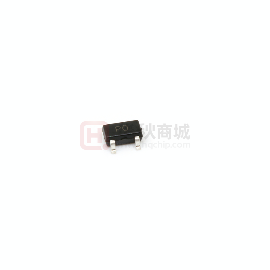
SOT-23-3
Features
VDS = 30V,ID = 5.8A
RDS(ON) < 45mΩ @ VGS=2.5V
RDS(ON) < 31mΩ @ VGS=4.5V
RDS(ON) < 27mΩ @ VGS=10V
High power and current handing capability
2
3
1
1. Gate 2.Source 3.Drain
Marking: P0
Applications
Load switch and in PWM applications
Power management
Schematic diagram
3Drain
1
Gate
2 Source
Absolute Maximum Ratings
Ratings at 25℃ ambient temperature unless otherwise specified.
Parameter
Symbol
Limit
Unit
Drain-Source Voltage
VDS
30
V
Gate-Source Voltage
VGS
±12
V
Drain Current-Continuous
ID
5.8
A
Drain Current-Pulsed Note1
IDM
30
A
Maximum Power Dissipation
PD
1.4
W
TJ,TSTG
150,-55 To 150
℃
RθJA
89
℃/W
Operating Junction and Storage Temperature Range
Thermal Characteristics
Thermal Resistance,Junction-to-Ambient Note2
www.pingjingsemi.com
Revision:1.0 May-2019
1/7
�PJM3400NSC
N- Enhancement Mode Field Effect Transistor
Electrical Characteristics
(TA=25℃ unless otherwise noted)
Parameter
Symbol
Condition
Min
Typ
Max
Unit
Drain-Source Breakdown Voltage
V(BR)DSS
VGS=0V ID=250μA
30
-
-
V
Zero Gate Voltage Drain Current
IDSS
VDS=30V,VGS=0V
-
-
1
μA
Gate-Body Leakage Current
IGSS
VGS=±12V,VDS=0V
-
-
±100
nA
VGS(th)
VDS=VGS,ID=250μA
0.7
0.9
1.4
V
VGS=2.5V, ID=4A
-
-
45
mΩ
VGS=4.5V, ID=5A
-
-
31
mΩ
VGS=10V, ID=5.8A
-
-
27
mΩ
VDS=5V,ID=5A
10
-
-
S
-
825
-
pF
-
100
-
pF
-
78
-
pF
-
3.3
-
nS
-
4.8
-
nS
-
26
-
nS
-
4
-
nS
-
10
-
nC
-
1.6
-
nC
-
3.1
-
nC
-
-
1.2
V
-
-
5.8
A
Static Characteristics
Gate Threshold
Voltage Note3
Drain-Source On-State Resistance Note3
Forward
Transconductance Note3
RDS(ON)
gFS
Dynamic Characteristics
Input Capacitance
Ciss
Output Capacitance
Coss
Reverse Transfer Capacitance
Crss
VDS=15V,VGS=0V,
f=1.0MHz
Switching Characteristics
Turn-on Delay Time
td(on)
Turn-on Rise Time
tr
Turn-Off Delay Time
td(off)
Turn-Off Fall Time
tf
Total Gate Charge
Qg
Gate-Source Charge
Qgs
Gate-Drain Charge
Qgd
VDD=15V, RL=2.7Ω
VGS=10V,RGEN=3Ω
VDS=15V,ID=5.8A,
VGS=4.5V
Drain-Source Diode Characteristics
Diode Forward Voltage Note3
Diode Forward Current
Note2
VSD
VGS=0V,IS=5.8A
IS
Notes:
1.
2.
3.
Repetitive Rating: Pulse width limited by maximum junction temperature.
Surface Mounted on FR4 Board, t ≤ 10 sec.
Pulse Test: Pulse Width ≤ 300μs, Duty Cycle ≤ 2%.
www.pingjingsemi.com
Revision:1.0 May-2019
2/7
�PJM3400NSC
N- Enhancement Mode Field Effect Transistor
PD Power(W)
ID- Drain Current (A)
Typical Characteristics Curves
TJ-Junction Temperature(℃)
TJ-Junction Temperature(℃)
Drain Current
ID- Drain Current (A)
Rdson On-Resistance(Ω)
Power Dissipation
ID- Drain Current (A)
Vds Drain-Source Voltage (V)
Drain-Source On-Resistance
ID- Drain Current (A)
Normalized On-Resistance
Output Characteristics
Vgs Gate-Source Voltage (V)
TJ-Junction Temperature(℃)
Transfer Characteristics
Drain-Source On-Resistance
www.pingjingsemi.com
Revision:1.0 May-2019
3/7
�C Capacitance (pF)
Rdson On-Resistance(Ω)
PJM3400NSC
N- Enhancement Mode Field Effect Transistor
Vds Drain-Source Voltage (V)
Rdson vs Vgs
Capacitance vs Vds
Vgs Gate-Source Voltage (V)
Is- Reverse Drain Current (A)
Vgs Gate-Source Voltage (V)
Qg Gate Charge (nC)
Vsd Source-Drain Voltage (V)
Gate Charge
Source- Drain Diode Forward
www.pingjingsemi.com
Revision:1.0 May-2019
4/7
�PJM3400NSC
N- Enhancement Mode Field Effect Transistor
Package Outline
SOT-23-3
Dimensions in mm
2.8
1.6
10
12
0.95
0.35
0.127± 0.03
± 0.01
A
±0.1
±0.05
2.92 ± 0.05
R0.15MAX
`4X
R0.15MAX
`4X
1.26MAX
0.06
12
± 0.05
± 0.03
0.65
1.1
± 0.05
10
Ordering Information
Device
PJM3400NSC
www.pingjingsemi.com
Revision:1.0 May-2019
Package
SOT-23-3
Shipping
3000/Reel&Tape(7inch)
5/7
�PJM3400NSC
N- Enhancement Mode Field Effect Transistor
Conditions of Soldering and Storage
Recommended condition of reflow soldering
(°C)
Peak Temperature
245 to 260°C, 10s max.
250
Reflow Heating Rate
1 to 5°C / s
Temperature
200
150
100
50
Pre Heating Rate
Preliminary Heating
1 to 5°C / s
130 to 170°C, 50 to 120s
Soldering
230°C, 20 to 30s
Cooling
60s min.
Figure
0
2 times max.
Recommended peak temperature is over 245 OC. If peak temperature is below 245 OC, you may adjust
the following parameters:
Time length of peak temperature (longer)
Time length of soldering (longer)
Thickness of solder paste (thicker)
Conditions of hand soldering
Temperature: 370 OC
Time: 3s max.
Times: one time
Storage conditions
Temperature
5 to 40 OC
Humidity
30 to 80% RH
Recommended period
One year after manufacturing
www.pingjingsemi.com
Revision:1.0 May-2019
6/7
�PJM3400NSC
N- Enhancement Mode Field Effect Transistor
Package Specifications
Cover Tape
3,000 pcs per reel
SOT-23-3
Carrier Tape
30,000 pcs per box
10 reels per box
240
217
0
21
43
5
120,000 pcs per carton
4 boxes per carton
455
220
2. Tape and reel data(7inch Units:mm)
D
A
3000
T2
T1
2900
2000
1900
1000
600
B
C
E
PS
F
1.10±0.10
Pin1
Revision:1.0 May-2019
N
3.2±0.10(Bo)
8 MAX
0.75
1.40±0.10(Ko)
B-B
Tape (8mm)
www.pingjingsemi.com
0.46
0.2
8 MAX
B
4.00±0.10
0.25±0.02(T)
2.45
1.55±0.05
3.50±0.05
2.00±0.05
8 ± 0 .1 0
4.00±0.10
B
1.75±0.10
Reel (7'')
Symbol
A
B
C
E
F
D
T1
T2
N
G
Value (unit: mm)
Ø 177.8±1
2.7±0.2
Ø 13.5±0.2
Ø 54.5±0.2
12.3±0.3
9.6+2/-0.3
1.0±0.2
1.2±0.2
3.15±0.1
1.22±0.1
7/7
�
很抱歉,暂时无法提供与“PJM3400NSC”相匹配的价格&库存,您可以联系我们找货
免费人工找货- 国内价格
- 10+0.19946
- 100+0.15591
- 300+0.13414
- 3000+0.11489
- 6000+0.10187
- 9000+0.09532